200mm Silicon Wafer Market Size and Share
Market Overview
| Study Period | 2020 - 2031 |
|---|---|
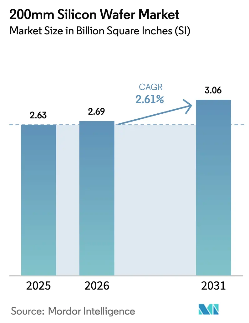
| Market Volume (2026) | 2.69 Billion Square Inches (SI) |
| Market Volume (2031) | 3.06 Billion Square Inches (SI) |
| Growth Rate (2026 - 2031) | 2.61% CAGR |
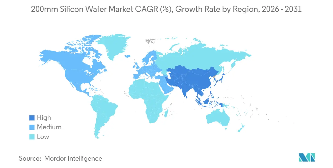
| Fastest Growing Market | Asia Pacific |
| Largest Market | Asia Pacific |
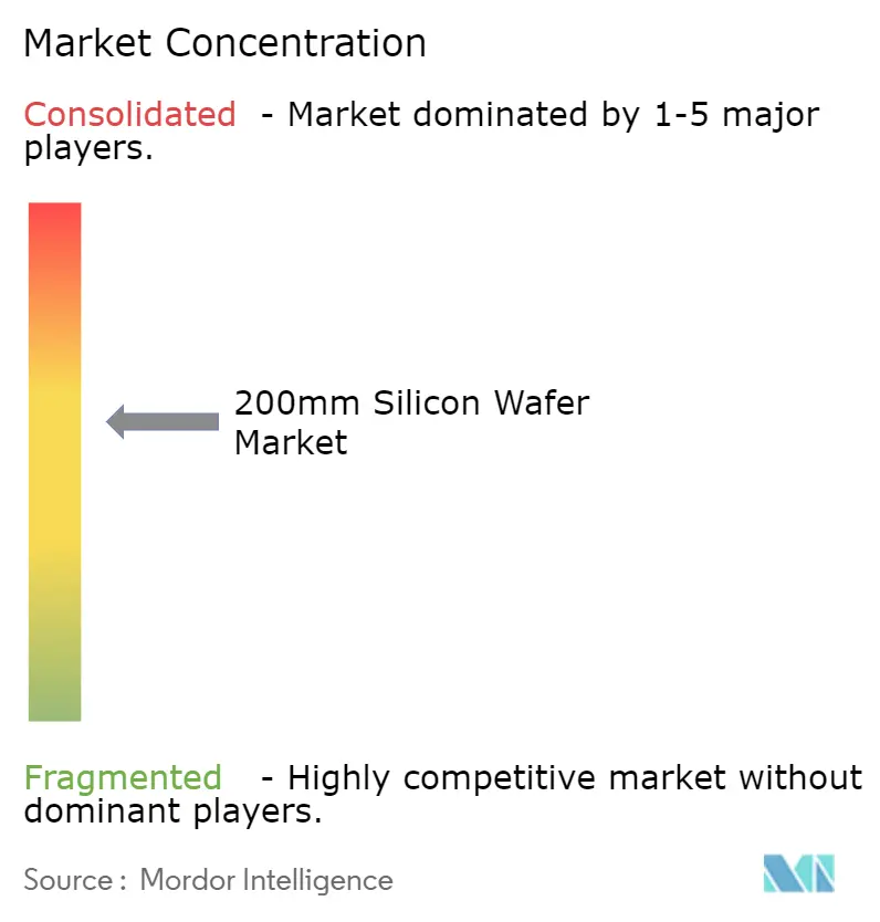
| Market Concentration | Medium |
Major Players *Disclaimer: Major Players sorted in no particular order Image © Mordor Intelligence. Reuse requires attribution under CC BY 4.0. | |
200mm Silicon Wafer Market Analysis by Mordor Intelligence
The 200mm silicon wafer market size is projected to be 2.69 billion square inches in 2026 and reach 3.06 billion square inches by 2031, growing at a CAGR of 2.61% from 2026 to 2031. Mature-node capacity is regaining strategic importance as automotive electrification expands, government incentives accelerate reshoring, and wide-bandgap devices shift to larger diameters. Refurbished 200mm tools that cost 40%-60% less than new equipment preserve the node’s cost advantage, while specialty substrates such as silicon carbide (SiC) and gallium nitride (GaN) extend its relevance in power electronics. Automotive and industrial suppliers continue locking in long-term 200mm allocations to avoid the supply shocks that upended production between 2021 and 2023, a pattern that supports stable utilization through the decade. At the same time, Wolfspeed’s 300mm SiC breakthrough hints at future margin compression, forcing 200mm producers to defend their position through yield improvements and substrate diversification.
Key Report Takeaways
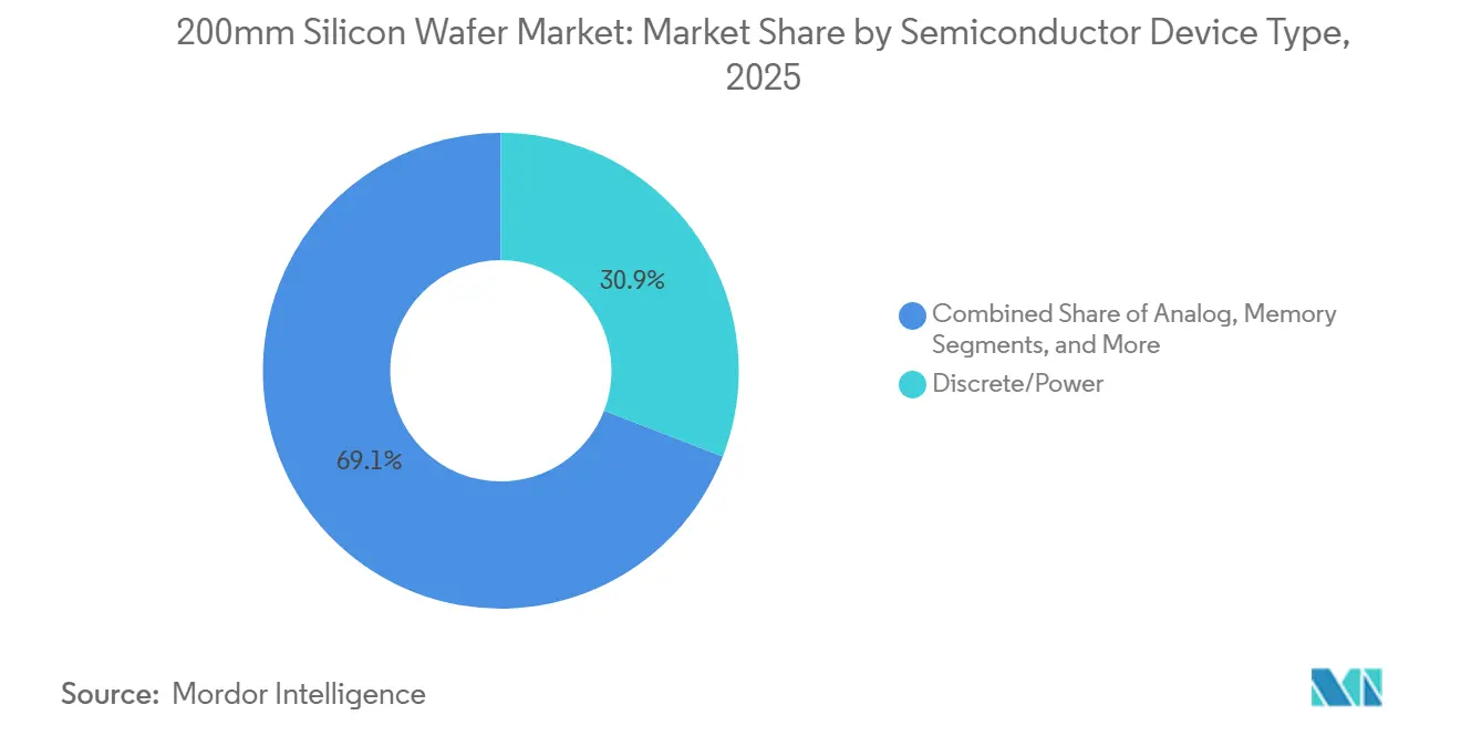
- By semiconductor device type, discrete and power devices led with 30.87% revenue share in 2025, while the category is forecast to expand at a 3.18% CAGR through 2031.
- By wafer type, specialty silicon accounted for the fastest 3.42% CAGR over 2026-2031.
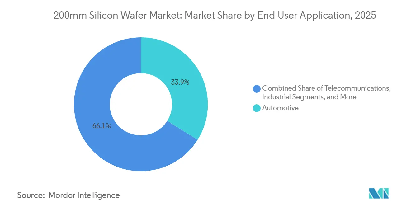
- By end-user, automotive captured 33.92% of the 200mm silicon wafer market share in 2025 and is advancing at a 4.31% CAGR to 2031.
- By region, Asia-Pacific held 79.23% of shipments in 2025; however, North American capacity is set to grow quickly as CHIPS Act projects ramp after 2026.
Note: Market size and forecast figures in this report are generated using Mordor Intelligence’s proprietary estimation framework, updated with the latest available data and insights as of January 2026.
Global 200mm Silicon Wafer Market Trends and Insights
Drivers Impact Analysis*
| Driver | (~) % Impact on CAGR Forecast | Geographic Relevance | Impact Timeline |
|---|---|---|---|
| Growing Demand for Automotive Power Semiconductors | +0.8% | Germany, United States, China, Japan | Medium term (2-4 years) |
| Migration of SiC and GaN Devices onto 200mm Platforms | +0.7% | North America, Europe, Asia-Pacific | Medium term (2-4 years) |
| Government Incentives for Mature-Node Reshoring | +0.5% | United States, European Union, Japan | Long term (≥ 4 years) |
| Expansion of IoT and Industrial Sensors | +0.4% | Global, led by Asia-Pacific | Long term (≥ 4 years) |
| Refurbished 200mm Equipment Deepens Cost Advantage | +0.2% | Global cost-sensitive markets | Short term (≤ 2 years) |
| Adoption of 200mm Wafers in Heterogeneous Chiplet Packaging | +0.2% | North America, Taiwan | Medium term (2-4 years) |
| Source: Mordor Intelligence | |||
Growing Demand for Automotive Power Semiconductors
Electric vehicles that adopt 800 V architectures require significantly larger SiC and insulated-gate bipolar transistor die areas than 400 V designs, lifting wafer starts per vehicle and tightening supply. STMicroelectronics and Sanan Optoelectronics are building capacity for 480,000 200mm SiC wafers per year in Catania to secure long-term traction-inverter demand.[1]STMicroelectronics, “SiC Joint Venture With Sanan Optoelectronics,” STMICROELECTRONICS.COM ON Semiconductor’s USD 2 billion Czech expansion similarly prioritizes EliteSiC devices, illustrating that Tier 1 suppliers are valuing surety of substrate supply over pure die cost. ROHM’s Miyazaki plant delivers 1.8 times the output of 150mm lines, bolstering Japan’s domestic sourcing resilience.[2]ROHM Semiconductor, “Miyazaki Plant SiC Production,” ROHM.COM Mitsubishi Electric’s April 2026 ramp in Kumamoto extends 200mm SiC supply to industrial motor drives and rail systems.[3]Mitsubishi Electric, “Kumamoto SiC Fabrication Facility,” MITSUBISHIELECTRIC.COM
Migration of SiC and GaN Devices onto 200mm Platforms
Bosch’s Roseville facility will ship 200mm SiC in 2026, giving the German firm vertical integration from crystal growth through module packaging.[4]Bosch, “Automotive Semiconductor Solutions,” BOSCH.COM Infineon’s Kulim migration encountered epitaxial yield issues but still reduced device cost by up to 35%, validating the economics of larger diameters. For GaN-on-silicon, GlobalFoundries leverages the thermal-mismatch benefits of 200mm to meet 5G radio power-amplifier tolerances.[5]GlobalFoundries, “GaN-on-Si Platforms,” GLOBALFOUNDRIES.COM Accelerated adoption compresses a decade-long roadmap into a three-year sprint, forcing equipment makers and substrate growers to scale simultaneously.
Government Incentives for Mature-Node Reshoring
The United States awarded GlobalWafers USD 406 million, Polar Semiconductor USD 123 million, and Texas Instruments USD 1.61 billion to expand domestic 200mm and specialty-substrate lines, offsetting capital costs and enforcing local-content rules. In Europe, Brussels is co-funding STMicroelectronics and Infineon, though stricter regional sourcing requirements could extend build times. These incentives aim to dilute Asia-Pacific’s 79.23% shipment dominance by 2030.
Expansion of IoT and Industrial Sensors
Global MEMS shipments exceeded 10 billion units in 2025, with Bosch Sensortec, TDK InvenSense, and STMicroelectronics leading output on 200mm lines where high tool utilization maintains cost leadership. Predictive-maintenance sensors now demand high-resistivity substrates above 1,000 Ω-cm, an area where 200mm vendors can match performance at lower input costs than 300mm fabs. Automotive safety features such as tire-pressure monitors further lock in AEC-Q100 qualified 200mm capacity.
Restraints Impact Analysis*
| Restraint | (~) % Impact on CAGR Forecast | Geographic Relevance | Impact Timeline |
|---|---|---|---|
| Scarcity and High Cost of Legacy 200mm Tools | -0.5% | North America, Europe, Asia | Short term (≤ 2 years) |
| High-Purity Polysilicon Price Volatility | -0.3% | Global, concentrated in Asia-Pacific | Short term (≤ 2 years) |
| Workforce Knowledge Attrition In Legacy Processes | -0.2% | North America, Europe, Japan | Medium term (2-4 years) |
| Supply-Chain Concentration Risk In East Asia | -0.2% | Automotive and industrial end-users worldwide | Long term (≥ 4 years) |
| Source: Mordor Intelligence | |||
Scarcity and High Cost of Legacy 200mm Tools
Applied Materials, ASML, and Tokyo Electron stopped shipping new 200mm toolsets more than a decade ago, so fabs now bid for refurbished equipment where prices climbed 30% between 2024 and 2025.[6]SEMI, “Legacy Equipment Market Trends,” SEMI.ORG Polar Semiconductor waited 12 months for legacy lithography steppers only to scrap 15% of shipments that failed acceptance tests, pushing project schedules and budgets. Limited transparency on tool pedigree elevates transaction risk, especially for high-density plasma etch modules where spare-part supply is scarce.
High-Purity Polysilicon Price Volatility
Spot polysilicon swung from USD 9 to USD 15 per kilogram during 2025 as solar overcapacity alternately flooded and withdrew supply, compressing wafer-maker margins locked into annual chip-fab contracts. Semiconductor-grade feedstock requires nine-nines purity and commands USD 15-USD 25 premiums, but that spread narrows when solar producers attempt to upgrade inventory during downturns. European wafer plants face extra exposure because electricity costs contribute up to 80 kWh per kilogram of polysilicon, a structural disadvantage versus Asia-Pacific peers.[7]Financial Times, “Energy Cost Impact On Silicon Supply,” FT.COM
*Our forecasts treat driver/restraint impacts as directional, not additive. The impact forecasts reflect baseline growth, mix effects, and variable interactions.
Segment Analysis
By Semiconductor Device Type: Power Devices Anchor Mature-Node Demand
Discrete and power devices represented 30.87% of the 200mm silicon wafer market size in 2025 and will post the segment’s best 3.18% CAGR through 2031. The migration of 800 V electric-vehicle systems expands SiC MOSFET and IGBT die areas, translating into sustained wafer demand. Logic remains tied to 90-nm to 180-nm nodes where 200mm retains capital efficiency, while NOR flash memory persists in safety-critical code storage.
Analog ICs favor 200mm because precision passives do not scale economically to 300mm. Texas Instruments is therefore using part of its USD 1.61 billion subsidy for additional analog output on 200mm lines. MEMS sensors and RF components lift optoelectronic demand, and the Universal Chiplet Interconnect Express standard now lets 200mm I/O dies integrate with 300mm compute chiplets, creating a hybrid demand stream.


By Wafer Type: Specialty Silicon Gains As RF And Sensor Applications Multiply
Prime polished substrates took 57.68% revenue in 2025, yet specialty silicon will expand at a 3.42% CAGR, the fastest in the 200mm silicon wafer market. High-resistivity silicon above 1,000 Ω-cm reduces RF loss in 5G switches, driving Soitec and Shin-Etsu Chemical to scale their proprietary crystal-pulling recipes. Epitaxial wafers underpin power devices, while silicon-on-insulator (SOI) supports automotive radar and battery-management ICs.
GlobalWafers is adding 200mm SiC epitaxy in Texas to diversify beyond commodity prime polished supply. High-resistivity production involves slower Czochralski pull speeds and elevated costs 40%-60% above standard grades. Sensor-grade substrates require precise (100) or (111) orientation, so device makers maintain dual sources to hedge supply risk.
By End-User Application: Automotive Electrification Reshapes Demand Mix
Automotive customers held 33.92% of the 200mm silicon wafer market share in 2025 and are projected to grow at 4.31% per year to 2031 as semiconductor content per vehicle doubles with advanced driver assistance and electrified powertrains. Bosch’s Roseville 200mm SiC line exemplifies vertical integration aimed at insulating EV modules from substrate shortages.
Industrial demand covers motor drives, robotics, and renewable inverters, retaining 200mm for rugged discrete devices and long product lifecycles. Consumer electronics contribute lower growth because advanced logic migrated to 300mm, yet audio and power-management circuits still prefer 200mm economics. Telecommunications infrastructure, especially 5G massive-MIMO base stations, uses GaN HEMTs and RF-SOI switches on 200mm, while aerospace and defense clients pay premiums for domestic traceability through Polar Semiconductor.
Geography Analysis
Asia-Pacific supplied 79.23% of global 200mm shipments in 2025, fueled by China’s USD 47.5 billion Big Fund Phase III that prioritizes mature-node self-sufficiency. National Silicon Industry Group and Zhonghuan Advanced Semiconductor are commissioning multiple 50,000-wafer-per-month lines, although export controls on advanced tools force reliance on refurbished equipment. Japan’s Shin-Etsu Chemical and SUMCO adjust 200mm output flexibly, catering to automotive clients that insist on domestic sourcing for resilience.
North America accounted for less than 10% of shipments in 2025 but is on track for the fastest absolute capacity gains as CHIPS Act funds flow to GlobalWafers, Bosch, and Polar Semiconductor. Texas Instruments’ mature-node buildout further lifts the region’s analog and power output, while Siltronic’s Portland plant supports specialty demand.
Europe’s 6%-8% share rests on STMicroelectronics’ Catania and Infineon’s Villach operations, now subsidized under the EU Chips Act. Energy-price volatility remains a headwind, but local sourcing mandates from automakers and industrial OEMs justify the cost premium. South America and the Middle East and Africa collectively represent under 2% of shipments, lacking indigenous 200mm capacity and relying on imports for automotive and telecom sectors.

Competitive Landscape
Shin-Etsu Chemical, SUMCO, GlobalWafers, Siltronic, and SK Siltron collectively commanded roughly 60% of shipments in 2025, giving the 200mm silicon wafer market a moderate level of concentration. Chinese entrants such as National Silicon Industry Group and Zhonghuan are capturing domestic prime-polished share by pricing 15%-25% below incumbents. Established suppliers respond by shifting toward high-margin specialty substrates; Soitec’s RF-SOI and GlobalWafers’ SiC epitaxy illustrate this pivot.
Intellectual-property filings in defect-free SiC epitaxy and high-resistivity doping are rising as vendors seek defensible advantages. Okmetic and Topsil serve niche float-zone silicon for high-voltage diodes, differentiating through customization rather than scale. Access to refurbished tool brokers in Japan and Taiwan enables incumbents to add selective capacity at 40%-60% lower capex than a new 300mm build, preserving return on invested capital.
Vertical integration is accelerating. STMicroelectronics partnered with Sanan Optoelectronics to internalize 200mm SiC output, while Bosch’s Roseville investment secures traction-inverter substrates. The emerging chiplet ecosystem provides a new addressable slice where 200mm wafers make interposers and analog tiles that couple with leading-edge compute dice, opening fresh revenue pools without head-to-head price competition.
200mm Silicon Wafer Industry Leaders
Shin-Etsu Handotai Co., Ltd.
SUMCO Corporation
GlobalWafers Co., Ltd.
Siltronic AG
SK Siltron Co., Ltd
- *Disclaimer: Major Players sorted in no particular order

Recent Industry Developments
- March 2026: Wolfspeed unveiled 300mm SiC wafers delivering 2.3 times more chips per wafer and 40% lower unit cost compared with 200mm formats, pressuring mid-decade cost curves.
- January 2026: Mitsubishi Electric began mass production at its Kumamoto 200mm SiC fab targeting industrial drives and rail systems.
- December 2026: GlobalWafers secured USD 406 million in CHIPS Act funds for a Texas plant that will produce 300mm silicon and 200mm SiC epitaxial wafers with a 2028 ramp target.
- October 2025: STMicroelectronics and Sanan Optoelectronics finalized a joint venture to produce 480,000 200mm SiC wafers annually in Catania for European and Asian power customers.


Global 200mm Silicon Wafer Market Report Scope
The 200mm Silicon Wafer Market Report is Segmented by Semiconductor Device Type (Logic, Memory, Analog, Discrete/Power, and Other Semiconductor Device Types (Optoelectronics, Sensors, Micro)), Wafer Type (Prime Polished, Epitaxial, Silicon-on-Insulator (SOI), Specialty Silicon (High-Resistivity, Power, Sensor-Grade)), End-User (Consumer Electronics, Industrial, Telecommunications, Automotive, Other End-user Applications), and Geography (North America, Europe, Asia-Pacific, South America, Middle East and Africa). The Market Forecasts are Provided in Terms of Shipment Area (Billion Square Inches).
| Logic |
| Memory |
| Analog |
| Discrete/Power |
| Other Semiconductor Device Types (Optoelectronics, Sensors, Micro) |
| Prime Polished |
| Epitaxial |
| Silicon-on-Insulator (SOI) |
| Specialty Silicon (High-Resistivity, Power, Sensor-Grade) |
| Consumer Electronics | Mobile and Smartphones |
| PCs and Servers | |
| Industrial | |
| Telecommunications | |
| Automotive | |
| Other End-User Applications |
| North America | United States |
| Canada | |
| Mexico | |
| Europe | Germany |
| United Kingdom | |
| France | |
| Rest of Europe | |
| Asia-Pacific | China |
| Japan | |
| India | |
| South Korea | |
| Taiwan | |
| Rest of Asia-Pacific | |
| South America | |
| Middle East and Africa |
| By Semiconductor Device Type | Logic | |
| Memory | ||
| Analog | ||
| Discrete/Power | ||
| Other Semiconductor Device Types (Optoelectronics, Sensors, Micro) | ||
| By Wafer Type | Prime Polished | |
| Epitaxial | ||
| Silicon-on-Insulator (SOI) | ||
| Specialty Silicon (High-Resistivity, Power, Sensor-Grade) | ||
| By End-User Application | Consumer Electronics | Mobile and Smartphones |
| PCs and Servers | ||
| Industrial | ||
| Telecommunications | ||
| Automotive | ||
| Other End-User Applications | ||
| By Geography | North America | United States |
| Canada | ||
| Mexico | ||
| Europe | Germany | |
| United Kingdom | ||
| France | ||
| Rest of Europe | ||
| Asia-Pacific | China | |
| Japan | ||
| India | ||
| South Korea | ||
| Taiwan | ||
| Rest of Asia-Pacific | ||
| South America | ||
| Middle East and Africa | ||


Key Questions Answered in the Report
What is the forecast CAGR for 200mm silicon wafer demand between 2026 and 2031?
Demand is projected to grow at a 2.61% CAGR over the 2026-2031 period.
Why are automotive suppliers investing in 200mm SiC capacity?
800 V electric-vehicle architectures need larger SiC die areas, so suppliers lock in 200mm allocations to secure substrate availability and cost advantages.
Which regions are adding the most new 200mm wafer fabs after 2026?
North America leads planned additions, buoyed by CHIPS Act funding for GlobalWafers, Bosch, Polar Semiconductor and Texas Instruments.
How does 200mm compare with 300mm for power semiconductor cost?
200mm SiC devices currently deliver 20%-35% lower unit cost than 150 mm lines, but Wolfspeed's 300 mm breakthrough may cut 200mm cost leadership by 40% once scaled.
What are the main restraints that could limit 200mm wafer supply?
Scarcity of legacy equipment, polysilicon price volatility, and retiring process engineers could slow capacity growth and raise execution risk.
Who are the top suppliers of 200mm silicon wafers by shipment share?
Shin-Etsu Chemical, SUMCO, GlobalWafers, Siltronic, and SK Siltron collectively account for about 60%-65% of global shipments.
Page last updated on:


