Industrial Semiconductor Silicon Wafer Market Size and Share
Market Overview
| Study Period | 2020 - 2031 |
|---|---|
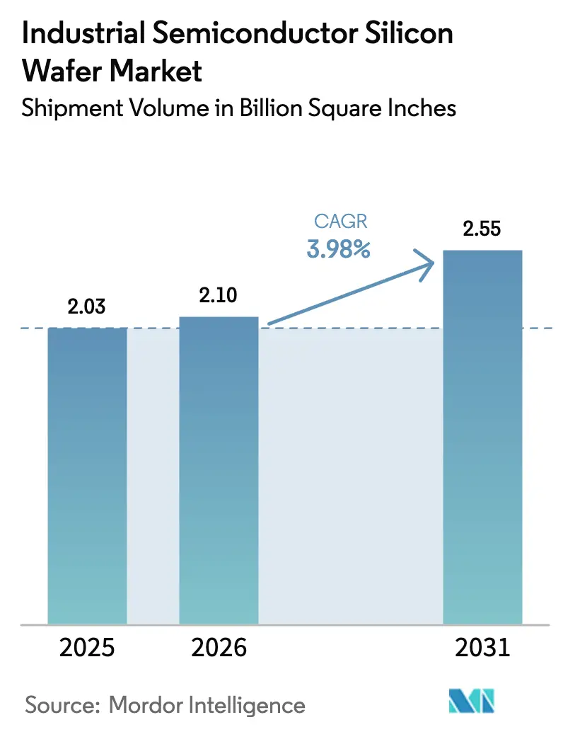
| Market Volume (2026) | 2.10 Billion Square Inches |
| Market Volume (2031) | 2.55 Billion Square Inches |
| Growth Rate (2026 - 2031) | 3.98% CAGR |
| Fastest Growing Market | Asia Pacific |
| Largest Market | Asia Pacific |
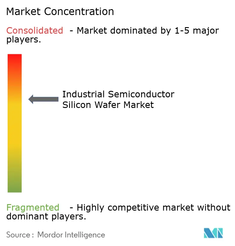
| Market Concentration | Medium |
Major Players *Disclaimer: Major Players sorted in no particular order Image © Mordor Intelligence. Reuse requires attribution under CC BY 4.0. | |
Industrial Semiconductor Silicon Wafer Market Analysis by Mordor Intelligence
The industrial semiconductor silicon wafer market size is projected to expand from 2.03 billion square inches in 2025 and 2.10 billion square inches in 2026 to 2.55 billion square inches by 2031, registering a CAGR of 3.98% between 2026 and 2031. Most of the incremental area will come from 300 mm substrates, which already account for nearly half of total consumption, while 200 mm epitaxial wafers for silicon-carbide (SiC) power devices and silicon-on-insulator (SOI) wafers for photonics accelerate their mix gains. A rebound in memory spending, tighter flatness requirements for gate-all-around logic, and inventory normalization in 2025 have together lifted shipment momentum. China’s record wafer investments, Europe’s push for supply-chain resilience, and the United States’ CHIPS Act subsidies are reshaping capacity decisions, often overriding pure cost considerations. Helium price spikes, 200 mm tool obsolescence, and packaging-induced warpage remain the chief operational risks. Meanwhile, incumbents use AI-based crystal-growth controls and reclaim initiatives to offset cost pressure and preserve margins.
Key Report Takeaways
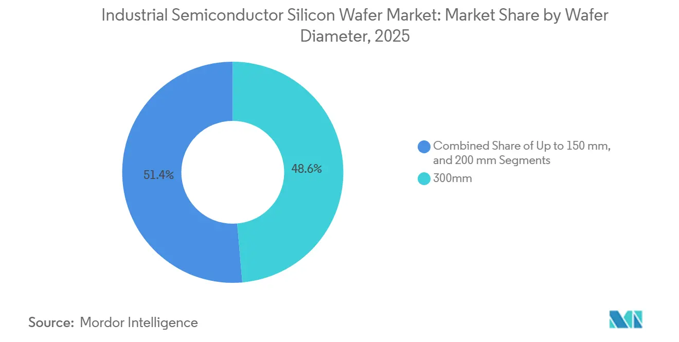
- By wafer diameter, 300 mm substrates commanded 48.62% revenue share of the industrial semiconductor silicon wafer market in 2025, while the segment is projected to expand at a 4.85% CAGR to 2031.
- By semiconductor device type, discrete and power devices held 30.21% of the industrial semiconductor silicon wafer market share in 2025, and they are forecast to post the fastest 4.55% CAGR through 2031.
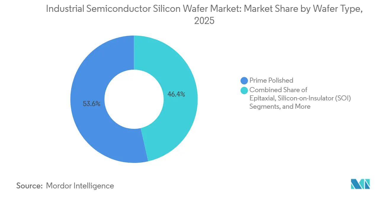
- By wafer type, prime polished wafers accounted for 53.58% of the industrial semiconductor silicon wafer market size in 2025; specialty silicon substrates, however, are advancing at a 4.31% CAGR and will narrow the gap by 2031.
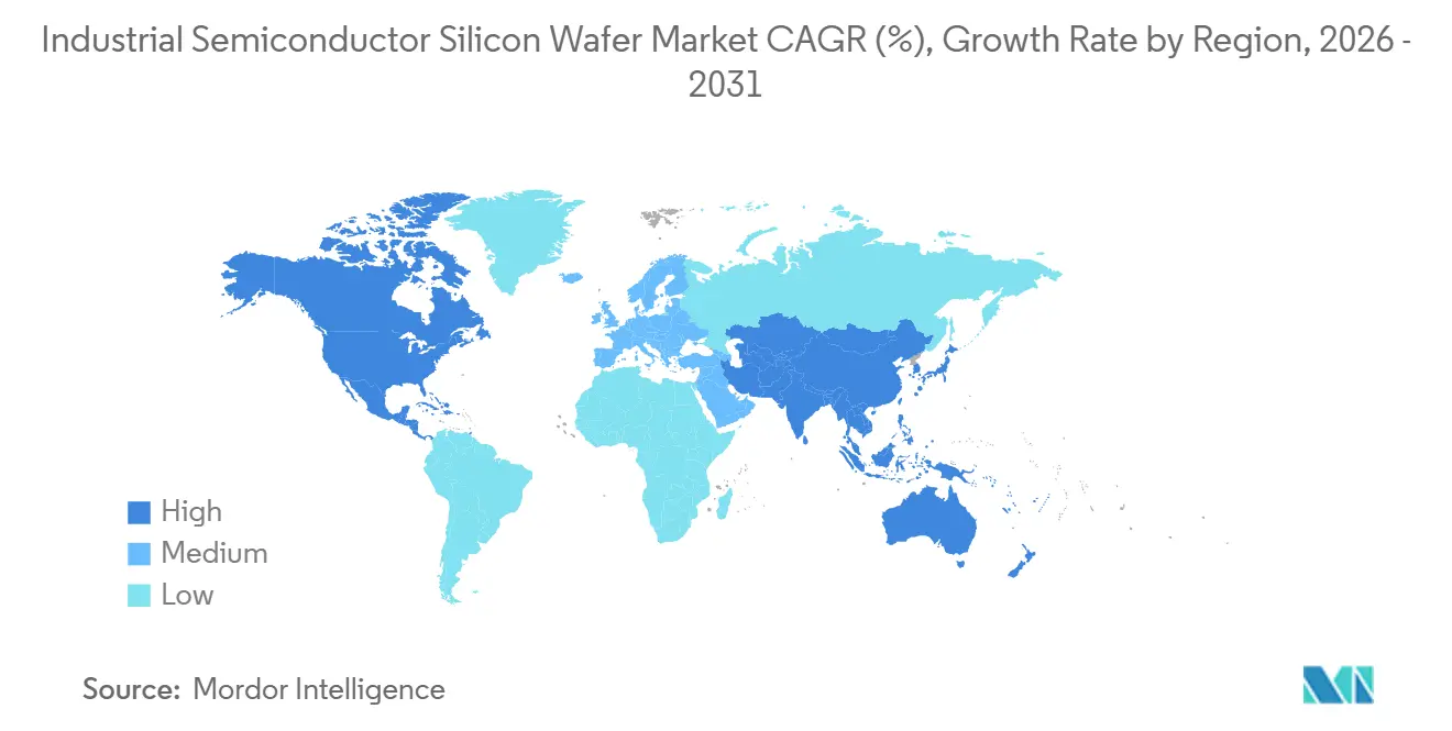
- By geography, Asia-Pacific contributed 82.39% of 2025 consumption and is on course for a 4.15% CAGR, far outpacing North America and Europe.
Note: Market size and forecast figures in this report are generated using Mordor Intelligence’s proprietary estimation framework, updated with the latest available data and insights as of January 2026.
Global Industrial Semiconductor Silicon Wafer Market Trends and Insights
Drivers Impact Analysis*
| Driver | (~) % Impact on CAGR Forecast | Geographic Relevance | Impact Timeline |
|---|---|---|---|
| Rising EV penetration and shift toward 800-V vehicle platforms | +1.2% | Global, notably China, Europe, North America | Medium term (2-4 years) |
| Rapid build-out of 800 V charging infrastructure | +0.8% | Europe, China, North America, spillover to South Korea, Japan | Medium term (2-4 years) |
| High-temperature, high-frequency advantages over silicon | +0.9% | APAC, Europe automotive and industrial nodes | Long term (≥ 4 years) |
| Government incentives for wide-band-gap fabs | +0.7% | North America, Europe, Japan | Short term (≤ 2 years) |
| AI-driven demand for 3D-IC silicon photonics | +0.6% | North America, Taiwan, China | Medium term (2-4 years) |
| Wafer reclaim and circular-economy mandates | +0.3% | Europe, North America | Long term (≥ 4 years) |
| Source: Mordor Intelligence | |||
Rising EV Penetration And Shift Toward 800-V Vehicle Platforms
Battery-electric models are migrating from 400-V to 800-V systems, which cuts charging time and wiring weight, but requires SiC MOSFETs processed on 200 mm epitaxial wafers. Infineon boosted 200 mm SiC yields by nearly 85% in 2024 through AI-optimized crystal growth, letting the firm double output without proportional capex. Wolfspeed achieved a 30% cost reduction in 200 mm SiC wafers that same year, widening the price gap with legacy silicon devices. Chinese brands BYD and NIO adopted 800 V early, locking in domestic substrate supply and extending global lead times beyond 26 weeks. Tight 200 mm availability is therefore an outgrowth of the EV transition and not merely a cyclical inventory issue.
Rapid Build-Out Of 800 V Charging Infrastructure
The European Alternative Fuels Infrastructure Regulation mandates high-power chargers every 60 km along core corridors by 2025, triggering more than 50,000 ultra-fast installations in 2024-2025.[1]European Commission, “Alternative Fuels Infrastructure Regulation,” ec.europa.euChina’s State Grid commissioned over 100,000 new 350 kW ports in 2025, each power module containing multiple SiC or GaN die. Charging-equipment makers such as ABB sign multiyear 200 mm wafer contracts to protect supply, further straining the spot market and reinforcing demand visibility.
High-Temperature, High-Frequency Advantages Over Silicon
SiC and GaN devices operate above 175 °C junction temperature and beyond 100 kHz switching frequency, unlocking smaller and lighter power supplies in data centers and industrial drives. Hyperscalers that swap silicon rectifiers for GaN converters cut rack-level cooling energy by up to 20%.[2]IEEE, “Thermo-Mechanical Stress in Advanced Packaging,” ieee.org Foundries are therefore reallocating 200 mm lines toward epitaxial and SOI variants even while prime polished area still dominates, locking in growth for specialty substrates.
Government Incentives For Wide-Band-Gap Fabs
Public subsidies are redrawing the wafer map. The United States awarded USD 1.5 billion to Wolfspeed for a 200 mm SiC fab and USD 750 million to SK Siltron for 300 mm silicon in Michigan. Japan’s Ministry of Economy, Trade and Industry backed Rapidus’ 2 nm pilot line with roughly USD 19 billion, while China’s “Big Fund” Phase III directs USD 27.8 billion toward wide-band-gap materials. Subsidies override cost-based site selection, creating regional overcapacity risks once funding sunsets.
Restraints Impact Analysis*
| Restraint | (~) % Impact on CAGR Forecast | Geographic Relevance | Impact Timeline |
|---|---|---|---|
| Limited availability of 200 mm substrates | -0.9% | Global, acute in automotive chains in Europe, North America, Japan | Short term (≤ 2 years) |
| Capital-intensive crystal-growth equipment | -0.7% | Global, most severe for new entrants in China, India, Southeast Asia | Medium term (2-4 years) |
| Packaging-induced thermo-mechanical stress | -0.4% | Taiwan, South Korea, North America | Medium term (2-4 years) |
| Looming helium supply constraints | -0.5% | Worldwide, severe in spot-helium reliant fabs | Short term (≤ 2 years) |
| Source: Mordor Intelligence | |||
Limited Availability Of 200 MM Substrates
Toolmakers have largely frozen new 200 mm equipment development, so fabs depend on refurbished lines with longer lead times, locking in a structural shortage. Okmetic’s 50,000-wafer capacity addition in Finland adds less than 2% to global demand and fails to ease 26-week automotive waits. As large IDMs migrate analog workloads to 300 mm, niche players face even tighter allocations.
Capital-Intensive Crystal-Growth Equipment
A top-end 300 mm Czochralski puller costs more than USD 15 million and ships after 18 months, limiting entries from smaller Chinese and Southeast Asian firms. Applied Materials and Tokyo Electron have full order books into 2027, which forces newcomers to rely on second-hand tools that struggle to meet sub-nanometer flatness for EUV processes. The divide cements incumbents’ edge in high-grade wafers while price competition intensifies in lower tiers.
*Our forecasts treat driver/restraint impacts as directional, not additive. The impact forecasts reflect baseline growth, mix effects, and variable interactions.
Segment Analysis
By Wafer Diameter: 300 MM Economies Drive Transition
The 300 mm portion of the industrial semiconductor silicon wafer market size commanded 48.62% in 2025 and is on track for a 4.85% CAGR as leading logic and memory fabs seek larger die counts per pass. Samsung and SK Hynix dedicated more than one-fifth of their DRAM starts to high-bandwidth memory in 2026, accelerating consumption of 300 mm blanks. Even analog IDMs now explore 300 mm conversions to escape 200 mm bottlenecks.
Smaller diameters retain relevance in RF, sensors, and optoelectronics where legacy tools suffice and capex is modest. However, hybrid bonding and through-silicon-via packaging demand the flatness tolerance achievable only on 300 mm substrates, effectively locking many advanced programs into the larger format. Chinese suppliers, led by National Silicon Industry Group, funnel fresh funding into commodity 300 mm grades, adding over 1 million wafers a month and challenging Japanese dominance.


By Semiconductor Device Type: Power Devices Outpace Logic
Discrete and power devices captured 30.21% of 2025 wafer area and will post the highest 4.55% CAGR as EVs and renewable inverters multiply. Each 800 V vehicle needs 50-100 SiC die made on 200 mm epi wafers, expanding substrate intensity even faster than vehicle volume. Logic continues to hold the largest absolute share but decelerates as only three global foundries pursue sub-3 nm nodes.
Memory shipments surge cyclically on the back of AI-driven HBM demand, yet the rebound is concentrated in a handful of hyper-scale-oriented fabs. Analog and sensor-interface ICs enjoy steady growth tied to industrial automation, while silicon photonics emerges as a niche but high-margin application that depends on ultra-flat SOI platforms, pushing specialized wafer orders higher.
By Wafer Type: Specialty Silicon Gains Share
Prime polished wafers still lead with 53.58% 2025 share, but specialty silicon is the fastest growing slice of the industrial semiconductor silicon wafer market at a 4.31% CAGR. Epitaxial layers provide dopant precision for SiC MOSFETs, and FD-SOI lowers leakage in automotive microcontrollers. High-resistivity wafers above 1,000 Ω-cm enable millimeter-wave RF circuits, while power-grade substrates limit oxygen defects in IGBTs.
China’s entry into 300 mm RF-SOI production in 2024 ended a near duopoly, forcing incumbents to differentiate through tighter thickness and lower particles. Reclaim initiatives in Europe now allow a 300 mm prime blank to be recycled up to five times, trimming effective cost by up to 40% and altering lifetime economics for test wafers.
Geography Analysis
Asia-Pacific represented 82.39% of worldwide consumption in 2025, and its 4.15% CAGR keeps the region firmly atop the industrial semiconductor silicon wafer market. China alone spent CNY 455 billion (USD 63.3 billion) on front-end capacity in 1H 2025, funneling more than half into substrates. Taiwan focuses on leading-edge logic, South Korea on memory, and Japan on wide-band-gap and SOI pilot lines.
North America remains smaller but grows quickly as CHIPS Act money underwrites GlobalWafers’ USD 3.5 billion Texas fab, with an additional USD 4 billion expansion announced the same year.[3] U.S. Department of Commerce, “CHIPS Act Funding Awards,” commerce.gov SK Siltron’s Michigan site, budgeted at USD 3.6 billion, will bring fresh 300 mm capacity by 2027. Canada and Mexico handle backend steps, which in turn drive demand for reclaimed or test wafers.
Europe stabilizes its share through the EUR 43 billion (USD 47.3 billion) Chips Act, supporting Siltronic’s EUR 2 billion (USD 2.2 billion) Fab-Next in Singapore for dual-region customers. Germany and France emphasize analog and power sovereignty, prolonging 200 mm relevance despite global 300 mm migration. Other regions together hold under 2% share but explore SiC initiatives tied to renewable power ambitions.

Competitive Landscape
Five suppliers Shin-Etsu Chemical, SUMCO, GlobalWafers, Siltronic, and SK Siltron controlled major share of global 300 mm shipments in 2025, creating pricing leverage in SOI and epi grades. Shin-Etsu posted FY 2025 revenue guidance of JPY 1.88 trillion (USD 16.49 billion), backed by full polysilicon-to-wafer integration. SUMCO’s planned 2026 closure of its Miyazaki plant will trim 200 mm output but free resources for higher-margin 300 mm expansions.
Chinese newcomers deploy scale and subsidies to erode share in commodity classes. National Silicon Industry Group and Zhonghuan together plan more than 1 million wafers per month of extra 300 mm output, contributing to an 8% decline in spot prices during 2025 even as shipments rose.[4]SEMI, “Spot Wafer Pricing Update,” semi.org Specialty micro-niches such as high-resistivity and reclaim offer refuge for smaller firms, with Wafer World’s January 2026 acquisition of Materials Research and Testing adding 50,000 reclaimed wafers per month.
Technology remains the decisive lever. Infineon’s AI-enabled yield gains and Wolfspeed’s 30% SiC cost cut illustrate how process leadership can trump sheer scale. Patent filings on wafer thinning, bonding, and stress mitigation jumped 40% between 2023 and 2025, signaling an innovation race to support chiplets and 3D stacks.
Industrial Semiconductor Silicon Wafer Industry Leaders
Shin-Etsu Chemical Co., Ltd.
SUMCO Corporation
GlobalWafers Co., Ltd.
Siltronic AG
SK Siltron Co., Ltd.
- *Disclaimer: Major Players sorted in no particular order

Recent Industry Developments
- March 2026: Qatar’s force majeure on helium exports raised Grade-A prices by 50%, prompting fabs to activate recycling systems to safeguard CMP and epi processes.
- January 2026: Wafer World acquired Materials Research and Testing, adding 50,000 monthly 300 mm reclaim capacity.
- December 2025: SK Siltron committed USD 1.5 billion to expand its Michigan 300 mm plant, bringing total U.S. outlay to USD 3.6 billion.
- October 2025: GlobalWafers opened a second 300 mm plant in Novara, Italy, rated at 200,000 wafers per month.


Global Industrial Semiconductor Silicon Wafer Market Report Scope
The industrial semiconductor silicon wafer market plays a critical role in the global semiconductor industry, serving as the foundational material for manufacturing various semiconductor devices. These wafers are essential for producing components used in electronics, automotive, telecommunications, and other industrial applications, thereby driving technological advancements and innovation.
The Industrial Semiconductor Silicon Wafer Market Report is Segmented by Wafer Diameter (Up to 150 mm, 200 mm, 300 mm), Semiconductor Device Type (Logic, Memory, Analog, Discrete, Other Types), Wafer Type (Prime Polished, Epitaxial, SOI, Specialty Silicon), and Geography (North America, Europe, Asia-Pacific, South America, Middle East, Africa). The Market Forecasts are Provided in Terms of Volume (Million Square Inches).
| Up to 150 mm |
| 200 mm |
| 300 mm |
| Logic |
| Memory |
| Analog |
| Discrete |
| Other Semiconductor Device Types (Optoelectronics, Sensors, Micro) |
| Prime Polished |
| Epitaxial |
| Silicon-on-Insulator (SOI) |
| Specialty Silicon (High-Resistivity, Power, Sensor-Grade) |
| North America | United States |
| Canada | |
| Mexico | |
| Europe | Germany |
| United Kingdom | |
| France | |
| Rest of Europe | |
| Asia-Pacific | China |
| Japan | |
| India | |
| South Korea | |
| Taiwan | |
| Rest of Asia-Pacific | |
| South America | |
| Middle East | |
| Africa |
| By Wafer Diameter | Up to 150 mm | |
| 200 mm | ||
| 300 mm | ||
| By Semiconductor Device Type | Logic | |
| Memory | ||
| Analog | ||
| Discrete | ||
| Other Semiconductor Device Types (Optoelectronics, Sensors, Micro) | ||
| By Wafer Type | Prime Polished | |
| Epitaxial | ||
| Silicon-on-Insulator (SOI) | ||
| Specialty Silicon (High-Resistivity, Power, Sensor-Grade) | ||
| By Geography | North America | United States |
| Canada | ||
| Mexico | ||
| Europe | Germany | |
| United Kingdom | ||
| France | ||
| Rest of Europe | ||
| Asia-Pacific | China | |
| Japan | ||
| India | ||
| South Korea | ||
| Taiwan | ||
| Rest of Asia-Pacific | ||
| South America | ||
| Middle East | ||
| Africa | ||


Key Questions Answered in the Report
What is the forecast CAGR for industrial semiconductor silicon wafer consumption through 2031?
Total shipped area is projected to expand at a 3.98% CAGR from 2026 to 2031.
How large will global wafer area reach by 2031?
Shipments are expected to rise to 2.55 billion square inches by 2031.
Why are 300 mm wafers gaining share over 200 mm alternatives?
They lower die cost per pass, meet tighter flatness specs for gate-all-around logic, and support high-bandwidth memory ramps, driving the segment’s 4.85% CAGR.
Which end-use device category is forecast to grow fastest in wafer demand?
Discrete and power devices, buoyed by 800 V electric vehicles and charging infrastructure, are set for a 4.55% CAGR.
How are government incentives influencing wafer supply geography?
U.S., European, and Japanese subsidy programs are pulling new fabs into higher-cost regions, creating domestic capacity that would not emerge under pure cost optimization.
What operational risks could disrupt wafer production in the near term?
Helium supply shocks, limited 200 mm tool availability, and packaging-induced warpage all threaten uptime and yields over the next two years.
Page last updated on:


