Silicon Wafer for Power Devices Market Size and Share
Market Overview
| Study Period | 2020 - 2031 |
|---|---|
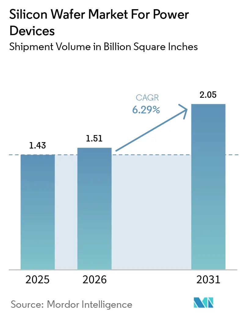
| Market Volume (2026) | 1.51 Billion Square Inches |
| Market Volume (2031) | 2.05 Billion Square Inches |
| Growth Rate (2026 - 2031) | 6.29% CAGR |
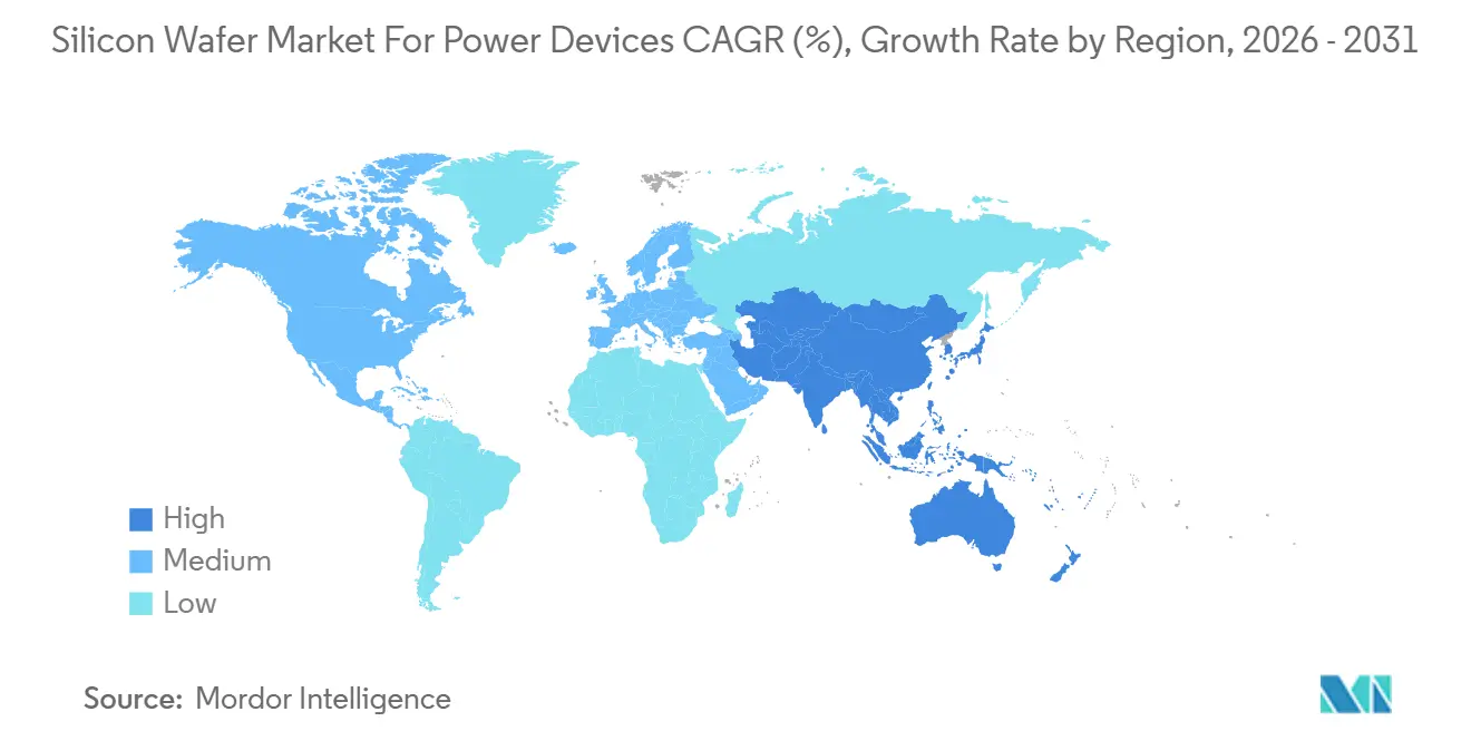
| Fastest Growing Market | Asia Pacific |
| Largest Market | Asia Pacific |
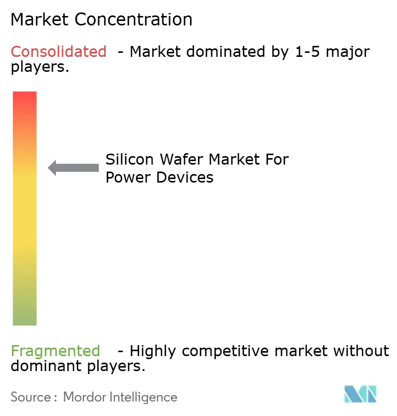
| Market Concentration | Medium |
Major Players *Disclaimer: Major Players sorted in no particular order Image © Mordor Intelligence. Reuse requires attribution under CC BY 4.0. | |
Silicon Wafer for Power Devices Market Analysis by Mordor Intelligence
The silicon wafer market for power devices was valued at 1.43 billion square inches in 2025 and is estimated to grow from 1.51 billion square inches in 2026 to reach 2.05 billion square inches by 2031, at a 6.29% CAGR during the forecast period from 2026 to 2031. Growth is anchored by vehicle electrification, renewable-energy grid upgrades, and the steady conversion of industrial drives from mechanical to electronic power control. Wide-bandgap materials, tighter export rules on epitaxial tools, and larger-diameter substrates are reshaping supply-chain strategies, while cost-reduction pressure is encouraging backward integration by integrated device manufacturers. The silicon wafer market is further influenced by polysilicon price swings that compress polished-wafer margins, although long-term contracts soften the impact for tier-one suppliers. Competitive intensity remains high as scale advantages in 300 mm lines converge with localization incentives in North America and Europe.
Key Report Takeaways
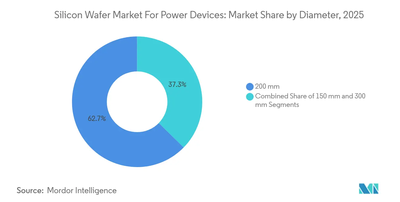
- By diameter, 200 mm substrates led with 62.68% of the market share in 2025, while 300 mm substrates is projected to expand at a 7.56% CAGR through 2031.
- By wafer type, epitaxial products accounted for 64.39% of the market share in 2025 and is forecast to grow at a 7.16% CAGR to 2031.
- By device type, MOSFETs held 46.78% the market share in 2025, whereas IGBTs is expected to record the highest growth at 7.65% CAGR through 2031.
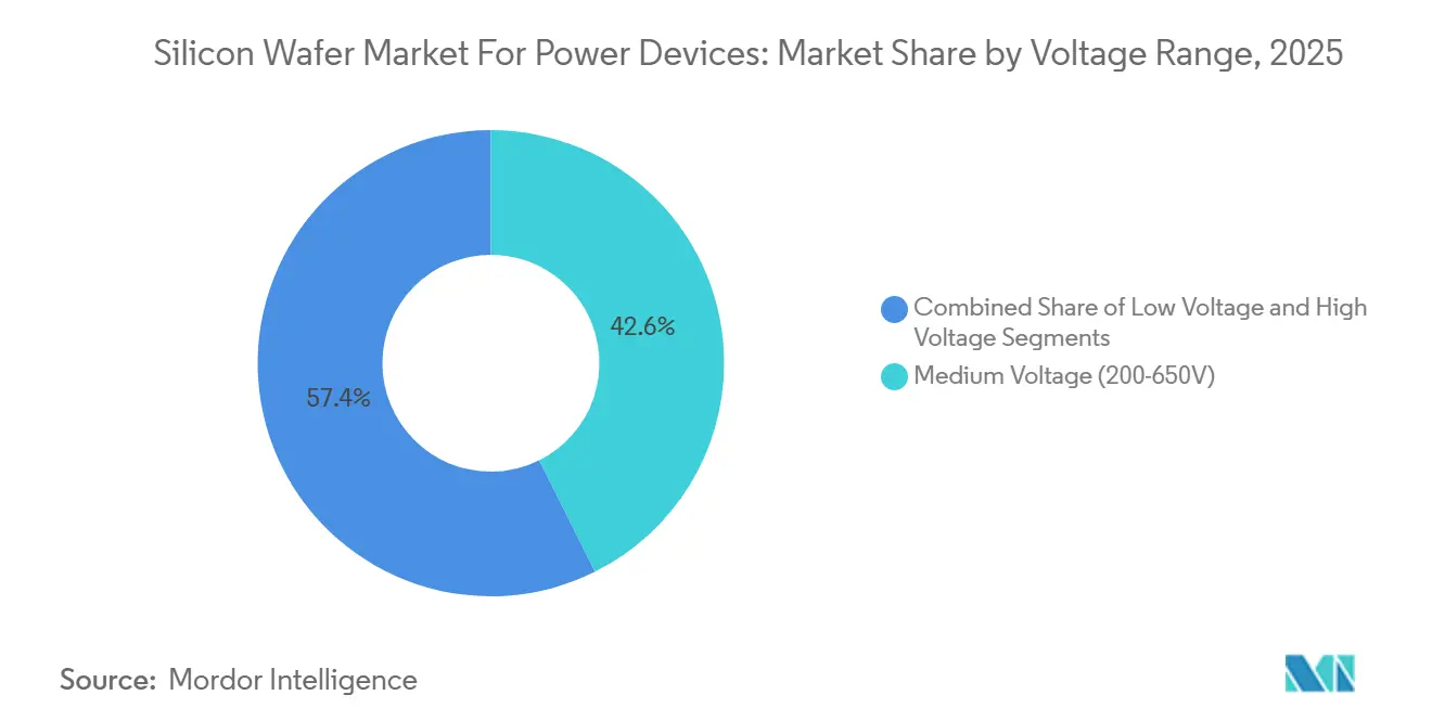
- By voltage range, medium-voltage wafers accounted for 42.63% of the market share in 2025, and high-voltage substrates are advancing at a 7.82% CAGR through 2031.
- By end-use, automotive applications commanded 38.76% of the market share in 2025 and led with an 8.32% CAGR over 2026-2031.
- By region, Asia-Pacific dominated with 69.98% of the market share in 2025 and is projected to post an 8.01% CAGR through 2031.
Note: Market size and forecast figures in this report are generated using Mordor Intelligence’s proprietary estimation framework, updated with the latest available data and insights as of January 2026.
Global Silicon Wafer for Power Devices Market Trends and Insights
Drivers Impact Analysis*
| Driver | (~) % Impact on CAGR Forecast | Geographic Relevance | Impact Timeline |
|---|---|---|---|
| EV-Led Demand Surge for High-Efficiency Power Conversion | +1.8% | Global, with concentration in China, Europe, North America | Medium term (2-4 years) |
| Renewable-Energy Build-Out Driving High-Voltage Inverter Wafers | +1.2% | Global, led by China, India, United States, Germany | Long term (≥ 4 years) |
| Shift to 300 mm Lines Lowering Cost Per Die | +1.5% | Asia-Pacific core, spill-over to North America and Europe | Long term (≥ 4 years) |
| Rising Industrial Automation and Electrified Factory Drives | +0.9% | Asia-Pacific, Europe, North America | Medium term (2-4 years) |
| On-Wafer Back-Side Vias Enabling Ultra-Thin Automotive Modules | +0.7% | Europe, North America, Japan | Short term (≤ 2 years) |
| AI-Driven In-Situ Metrology Freeing Latent Epi Capacity | +0.5% | Global, early adoption in Japan, Taiwan, South Korea | Short term (≤ 2 years) |
| Source: Mordor Intelligence | |||
EV-Led Demand Surge for High-Efficiency Power Conversion
Electric vehicles are shifting from 400-volt to 800-volt battery platforms, cutting fast-charge times to under 20 minutes and reducing wiring mass. SiC MOSFETs switching above 20 kHz replace multiple silicon switches, shrinking passive components and lowering total inverter cost even at a wafer premium. Automakers in China, Europe, and the United States are vertically integrating SiC device production to secure substrate supply and capture additional margin, reinforcing multi-year wafer demand growth.[1]Hyundai Motor Group, “800V Battery System and Ultra-Fast Charging Technology,” hyundaimotorgroup.com The International Energy Agency projects battery-electric and plug-in hybrid sales of 17 million units in 2026, which equates to roughly 50 million square inches of epitaxial SiC wafers. This demand underpins sustained expansion of the silicon wafer market across the automotive value chain.
Renewable-Energy Build-Out Driving High-Voltage Inverter Wafers
Utility-scale solar and offshore wind installations operate at direct-current bus voltages between 1,000 and 1,500 volts, pushing power-device ratings beyond 1,700 volts. In 2025 the United States added 35 GW of solar and 12 GW of wind capacity, translating into nearly 80 million square inches of high-voltage substrates for inverter modules.[2]U.S. Energy Information Administration, “Electric Power Monthly February 2025,” eia.gov Emerging markets such as India are matching this trajectory through multi-gigawatt annual targets, each paired with inverter efficiency mandates that favor SiC devices. European auctions now stipulate stringent harmonic-distortion thresholds, further accelerating the adoption of thick-epi wafers with low defect densities. These policies collectively reinforce the silicon wafer market’s momentum in high-voltage segments.
Shift to 300 mm Lines Lowering Cost Per Die
Moving from 200 mm to 300 mm wafers increases usable area more than twofold while raising clean-room cost by roughly half, yielding a 30-40% reduction in cost per die once yields stabilize. The first commercially qualified 300 mm SiC wafer achieved comparable defect density to 200 mm formats and offers 2.3 times the die output. The scale benefit reshapes competitive dynamics because early adopters can undercut prices yet preserve margins above 35%. Standard-setting bodies are tightening bow and thickness specifications, and advanced metrology now mitigates yield loss by double-digit percentages, opening a clear path to high-volume manufacturing.
Rising Industrial Automation and Electrified Factory Drives
Manufacturers are electrifying robots, conveyor systems, and servo drives in pursuit of productivity and energy savings. Global robot installations reached 553,000 units in 2024, and each multi-axis drive consumes Si-based or SiC die area for switching elements. Servo inverters rated between 400 and 690 volts increasingly adopt SiC MOSFETs to achieve efficiencies above 98%, which lowers cooling loads and operating costs. Government programs in China and Europe that fund smart-factory upgrades indirectly stimulate wafer demand, keeping the silicon wafer market on a strong uptrend through capital-equipment cycles.
Restraints Impact Analysis*
| Restraint | (~) % Impact on CAGR Forecast | Geographic Relevance | Impact Timeline |
|---|---|---|---|
| Polysilicon Feedstock Price Volatility | -0.8% | Global, acute in regions with limited vertical integration | Short term (≤ 2 years) |
| USD 1 Billion+ CAPEX Barrier for 200-300 mm SiC Wafer Fabs | -1.2% | Global, constraining new entrants in North America, Europe, Asia-Pacific | Long term (≥ 4 years) |
| Thermo-Mechanical Bow in 300 mm SiC Wafers Slashing Yields | -0.6% | Asia-Pacific, North America early adopters | Medium term (2-4 years) |
| Export-Control Uncertainty for Next-Gen Epi Reactors | -0.5% | China, with indirect effects on global supply chains | Medium term (2-4 years) |
| Source: Mordor Intelligence | |||
Polysilicon Feedstock Price Volatility
Spot polysilicon prices fell from USD 30 per kg in early 2023 to USD 6-8 per kg by late 2024, compressing polished-wafer gross margins by up to eight percentage points. Suppliers locked into higher long-term contracts faced opportunity costs when spot buyers undercut their pricing. Trade investigations on dumping added tariff uncertainty, raising procurement risk and hindering short-term planning. Although epitaxial-grade suppliers can absorb some variance through premiums, sustained volatility dampens investment appetite and can slow wafer-capacity additions in cost-sensitive segments.
USD 1 Billion+ CAPEX Barrier for 200-300 mm SiC Wafer Fabs
A greenfield 200 mm SiC facility capable of 100,000 wafers per year now requires at least USD 1 billion. Even with government subsidies covering about 15% of project cost, the remaining capital must weather rising interest rates and long equipment lead times.[3]U.S. Department of Commerce, “CHIPS and Science Act Funding Awards,” commerce.gov Smaller entrants therefore pivot to joint ventures or licensing, which spread risk but dilute margins. The financing hurdle narrows the supplier base, raises switching costs for customers, and slows the geographic diversification of the silicon wafer market until additional public-private incentives emerge.
*Our forecasts treat driver/restraint impacts as directional, not additive. The impact forecasts reflect baseline growth, mix effects, and variable interactions.
Segment Analysis
By Diameter: 300 mm Substrates Unlock Scale Economies
The 200 mm category retained 62.68% of the silicon wafer market for power devices in 2025, reflecting legacy fab infrastructure that remains cost-effective for medium-power devices. Yet the 300 mm class is forecast to post a 7.56% CAGR as automotive tier-ones demand larger die counts per wafer to amortize clean-room overhead. Early production runs already demonstrate 2.3-times usable die with comparable defect density, confirming that learning curves are steep enough to sustain the silicon wafer market size advantages at larger diameters.
Yield drag from thermo-mechanical bow above 50 µm still limits immediate mass adoption, but standards groups are driving thickness-variation targets below 2 µm. Back-side ion implantation and optimized epitaxy recipes are showing double-digit yield gains, suggesting that volume tipping points will arrive within four years. Scale leaders able to master bow control will hold durable cost positions across the silicon wafer market.


By Wafer Type: Epitaxial Layers Drive Performance Differentiation
Epitaxial wafers captured 64.39% of the market share in 2025 on the strength of trench-gate MOSFET migration, and they are set to advance at a 7.16% CAGR. Precise doping and thickness uniformity enable lower on-resistance and higher switching speeds, attributes essential to automotive and renewable-energy power trains. Tight integration between deposition tools and AI-assisted metrology now lifts tool utilization from 75% to 85%, freeing latent capacity that underpins a resilient silicon wafer market size at the premium end.
Polished substrates remain relevant in diodes and legacy thyristors, where value thresholds are low but margin pressure is increasing due to polysilicon price shocks. Suppliers operating in both polished and epitaxial segments mitigate risks effectively. However, sustained growth is clearly shifting toward high-specification epitaxy, emphasizing its strategic importance within the broader silicon wafer market.
By Device Type: IGBT Growth Outpaces MOSFET in High-Power Segments
MOSFETs held 46.78% of the silicon wafer market for power devices in 2025, serving low- to medium-voltage systems that leverage their fast switching characteristics. IGBTs, however, are expected to grow at a 7.65% CAGR because they deliver robust short-circuit capability above 1,200 volts, ideal for industrial drives and large traction inverters. As system designers balance switching frequency, conduction loss, and cost, the silicon wafer market share mix will remain fluid.
Press-pack diodes and legacy thyristors are losing relevance, but demand for anti-parallel diodes tied to each IGBT or MOSFET switch is stabilizing wafer volumes. The distinction between high-voltage MOSFETs and IGBTs is diminishing as new SiC MOSFET generations achieve 10 mΩ on-resistance. This shift is driving suppliers to offer co-design services that align wafer recipes with end-system targets, strengthening customer lock-in across the silicon wafer market.
By Voltage Range: High-Voltage Segment Captures Renewable-Energy Build-Out
Medium-voltage substrates between 200 and 650 volts represented 42.63% of the market share in 2025, driven by consumer electronics, telecom, and light industrial drives. High-voltage wafers above 650 volts are growing faster at 7.82% CAGR, buoyed by grid-connected solar inverters and wind converters that require blocking voltages beyond 1,700 volts. Inverter efficiency mandates beyond 98.5% set by regulators create a demand bridge that draws SiC epitaxy further into mainstream production, raising the silicon wafer market size for power devices in high-voltage tiers.
Low-voltage wafers, typically under 200 volts, continue to play a role in data-center power distribution and 48-volt mild hybrids. However, many of these applications are transitioning to GaN-on-silicon. Renewable energy trends are reshaping voltage-range priorities, requiring next-generation wafers to balance thicker epi layers with acceptable yield to remain competitive in the silicon wafer market.
By End-Use Industry: Automotive Electrification Dominates Incremental Demand
Automotive applications consumed 38.76% of the silicon wafer market for power devices in 2025 and is forecasted to expand at an 8.32% CAGR through 2031. Each battery-electric vehicle typically integrates SiC die area across traction inverters, on-board chargers, and DC-DC converters, translating to roughly 3 square inches of wafers per unit. Scaling EV sales, therefore, magnifies substrate requirements, cementing this vertical as the primary growth engine for the silicon wafer market.
Industrial automation remains the second largest user, with factory electrification pushing servo drives toward higher switching frequencies. Renewable energy and large-scale storage comprise a high-teens share, yet grid modernization initiatives suggest upside. Consumer appliances and telecom power systems form the balance of demand, growing at steady but modest rates. Automotive-led growth thus sets the cadence for capacity additions and technology roadmaps across the silicon wafer market.
Geography Analysis
Asia-Pacific commanded 69.98% of the market share in 2025 and is projected to post an 8.01% CAGR through 2031. Expansion programs by China’s National Silicon Industry Group, Japan’s investments in 300 mm polishing lines, and South Korea’s SiC capacity additions create a formidable ecosystem that anchors the silicon wafer market. Government robotics, EV, and renewable-energy targets further reinforce regional demand, ensuring that local fabs operate near full utilization.
North America is experiencing an investment surge catalyzed by CHIPS Act incentives and automotive localization goals. New facilities in New York, North Carolina, and Texas reduce dependence on imports, diversify supply risk, and embed advanced 300 mm processes closer to end-markets. The region’s policy environment, combined with access to leading semiconductor equipment suppliers, positions it as a credible secondary hub in the silicon wafer market.
Europe leverages the European Chips Act and stringent vehicle-emission rules to claim a larger share of global power-device production. Expansion projects in Germany and Italy emphasize SiC epitaxy and 300 mm silicon, supported by multi-billion-dollar public funding. Collaborative platforms focused on engineered substrates and ultra-thin wafers illustrate Europe’s strategy of technology differentiation rather than cost leadership. South America and the Middle East and Africa remain import-oriented today, yet early initiatives signal long-term ambitions to establish regional substrate capabilities.

Competitive Landscape
The silicon wafer market is moderately concentrated. Large integrated device manufacturers such as Infineon, STMicroelectronics, and onsemi are backward-integrating to secure wafers and extract additional margin, compressing opportunities for pure-play substrate houses. Early mastery of 300 mm SiC production delivers a cost edge of up to 40%, allowing first movers to reset price benchmarks without eroding profitability.
Joint-venture models are proliferating across Japan and Europe as mid-tier suppliers pool capital to clear billion-dollar investment hurdles. While such alliances lower financial risk, they can slow decision-making and limit proprietary process control. Chinese entrants, supported by domestic subsidies, ramp 200 mm SiC lines aimed at cost-sensitive markets but face export-control challenges on advanced epitaxy tools, constraining penetration into premium automotive supply chains.
Innovation focus has shifted to ultra-thin and engineered substrates. Demonstrations of 20-µm silicon and silicon-on-insulator wafers prove that substrate thickness can directly halve on-resistance and improve thermal paths, creating monetizable system-level benefits. Vendors offering application-specific wafer design support are increasingly viewed as strategic partners rather than commodity suppliers, a trend that tightens long-term offtake agreements and raises switching costs for customers.
Silicon Wafer for Power Devices Industry Leaders
Shin-Etsu Chemical
SUMCO Corporation
GlobalWafers Co., Ltd.
SK Siltron Co., Ltd.
Soitec S.A.
- *Disclaimer: Major Players sorted in no particular order

Recent Industry Developments
- January 2026: Wolfspeed announced commercial qualification of a 300 mm SiC wafer with defect density below 1 defect/cm², delivering a 30-40% cost-per-die reduction.
- November 2025: STMicroelectronics committed EUR 730 million (USD 800 million) to triple SiC substrate capacity at its Catania, Italy site by 2027.
- September 2025: Infineon Technologies began production at its expanded Kulim, Malaysia fab, adding 200 mm SiC capacity for automotive and industrial devices.
- July 2025: GlobalWafers obtained a USD 400 million CHIPS Act grant to build a 300 mm silicon wafer facility in Sherman, Texas, with output slated for 2028.


Global Silicon Wafer for Power Devices Market Report Scope
Silicon wafers are thin slices of semiconductor material, primarily silicon, used as a substrate for fabricating power devices. These wafers serve as the foundation for creating various electronic components, including diodes, MOSFETs, and IGBTs, which are essential in power management and energy conversion applications.
The Silicon Wafer Market for Power Devices Report is Segmented by Diameter (150 mm, 200 mm, and 300 mm), Wafer Type (Polished, and Epitaxial), Device Type (IGBT, MOSFET, Diode, Thyristor), Voltage Range (Low Voltage, Medium Voltage, and High Voltage), End-Use Industry (Automotive, Industrial and Automation, Renewable Energy and Energy Storage, Consumer and Appliance Power, and Telecom and Infrastructure Power Systems), and Geography (North America, Europe, Asia-Pacific, South America, and Middle East and Africa). The Market Forecasts are Provided in Terms of Volume (Square Inches).
| 150 mm |
| 200 mm |
| 300 mm |
| Polished |
| Epitaxial |
| IGBT |
| MOSFET |
| Diode |
| Thyristor |
| Low Voltage (Less than 200V) |
| Medium Voltage (200-650V) |
| High Voltage (Above 650V) |
| Automotive |
| Industrial and Automation |
| Renewable Energy and Energy Storage |
| Consumer and Appliance Power |
| Telecom and Infrastructure Power Systems |
| North America | United States |
| Canada | |
| Mexico | |
| Europe | Germany |
| United Kingdom | |
| France | |
| Rest of Europe | |
| Asia-Pacific | China |
| Japan | |
| India | |
| South Korea | |
| Taiwan | |
| Rest of Asia-Pacific | |
| South America | |
| Middle East and Africa |
| By Diameter | 150 mm | |
| 200 mm | ||
| 300 mm | ||
| By Wafer Type | Polished | |
| Epitaxial | ||
| By Device Type | IGBT | |
| MOSFET | ||
| Diode | ||
| Thyristor | ||
| By Voltage Range | Low Voltage (Less than 200V) | |
| Medium Voltage (200-650V) | ||
| High Voltage (Above 650V) | ||
| By End-Use Industry | Automotive | |
| Industrial and Automation | ||
| Renewable Energy and Energy Storage | ||
| Consumer and Appliance Power | ||
| Telecom and Infrastructure Power Systems | ||
| By Geography | North America | United States |
| Canada | ||
| Mexico | ||
| Europe | Germany | |
| United Kingdom | ||
| France | ||
| Rest of Europe | ||
| Asia-Pacific | China | |
| Japan | ||
| India | ||
| South Korea | ||
| Taiwan | ||
| Rest of Asia-Pacific | ||
| South America | ||
| Middle East and Africa | ||


Key Questions Answered in the Report
How fast is demand for power-device substrates growing in automotive applications?
Automotive segment is projected to rise at an 8.32% CAGR through 2031 as 800-volt battery architectures accelerate SiC adoption.
What is the main cost advantage of moving to 300 mm wafers?
A 2.25-times area increase delivers up to 40% lower cost per die once yields stabilize, positioning early adopters for durable pricing power.
Why are high-voltage wafers gaining share in renewable-energy systems?
Grid-connected solar and wind converters now run at 1,000-1,500 volts, which demands devices rated ≥1,700 volts, driving wafer thickness and epitaxy requirements upward.
Which regions dominate substrate manufacturing capacity today?
Asia-Pacific holds nearly 70% of global volume, though North America and Europe are adding capacity under CHIPS-aligned subsidy programs.
How does polysilicon volatility influence wafer suppliers?
A drop from USD 30 to USD 6-8 per kg slashed margins for polished-wafer vendors, forcing capacity adjustments and favoring vertically integrated producers.
What investment threshold limits new entrants in SiC wafer production?
Building a 200 mm SiC fab with 100,000-wafer annual output requires at least USD 1 billion, a barrier mitigated only partially by government incentives.
Page last updated on:


