300mm Silicon Wafer Market Size and Share
Market Overview
| Study Period | 2020 - 2031 |
|---|---|
| Market Volume (2026) | 9.71 Billion Square Inches (SI) |
| Market Volume (2031) | 12.97 Billion Square Inches (SI) |
| Growth Rate (2026 - 2031) | 5.96% CAGR |
| Fastest Growing Market | Asia Pacific |
| Largest Market | Asia Pacific |
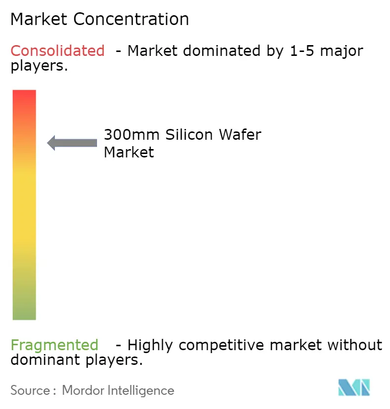
| Market Concentration | High |
Major Players *Disclaimer: Major Players sorted in no particular order Image © Mordor Intelligence. Reuse requires attribution under CC BY 4.0. | |
300mm Silicon Wafer Market Analysis by Mordor Intelligence
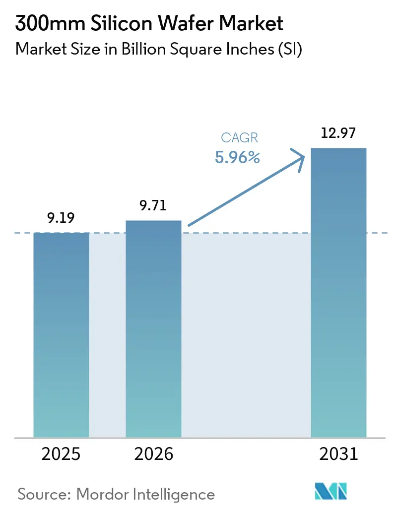
The 300mm silicon wafer market size is projected to be 9.19 billion square inches in 2025, 9.71 billion square inches in 2026, and reach 12.97 billion square inches by 2031, growing at a 5.96% CAGR from 2026 to 2031. Demand stems from artificial intelligence accelerators, data-center expansion, and automotive electrification, all of which require dense transistor architectures that only 300 mm substrates cost-effectively support at scale. Tight equipment lead times and polysilicon price volatility hinder near-term capacity additions, yet multi-year capital programs at major foundries continue to lock in future output. Intensifying geopolitical subsidies reshape the footprint of the 300mm silicon wafer market, fragmenting the traditionally Asia-centric supply chain into several regional hubs. Meanwhile, technical barriers to 450 mm transition anchor 300 mm as the de-facto standard through at least 2035.
Key Report Takeaways
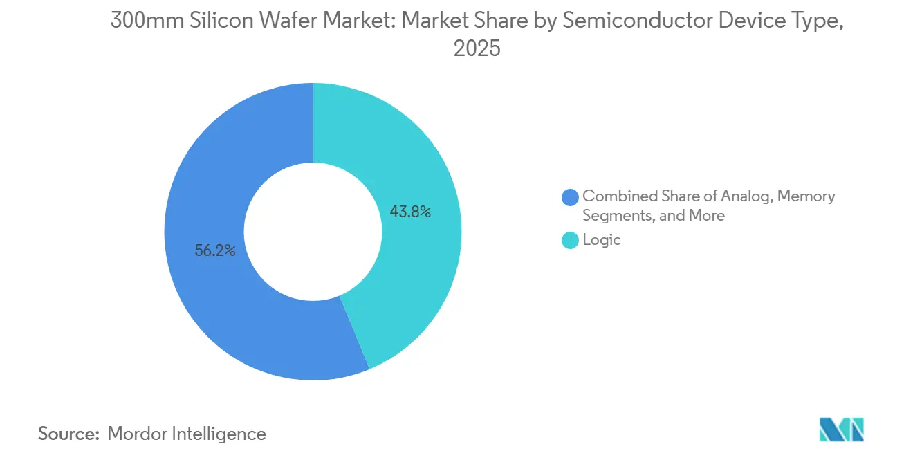
- By semiconductor device type, logic held 43.76% of the 300mm silicon wafer market share in 2025, while logic is projected to expand at a 6.11% CAGR through 2031.
- By wafer type, prime-polished substrates accounted for 82.68% of the 300mm silicon wafer market size in 2025, and silicon-on-insulator substrates are advancing at a 7.01% CAGR through 2031.
- By end-user, consumer electronics led with 43.83% of shipments in 2025, whereas automotive applications were expected to record the fastest growth with an 8.29% CAGR to 2031.
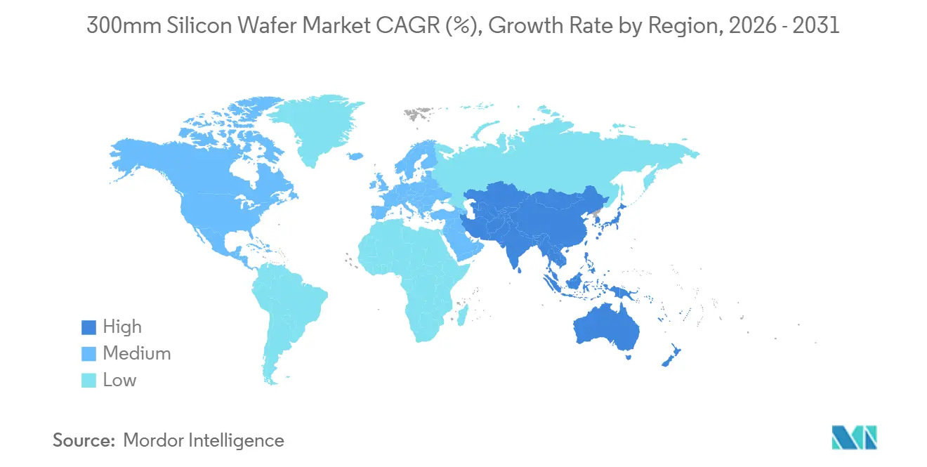
- By geography, Asia-Pacific commanded 79.67% of global shipments in 2025 and is expected to post a 6.06% CAGR between 2026 and 2031.
Note: Market size and forecast figures in this report are generated using Mordor Intelligence’s proprietary estimation framework, updated with the latest available data and insights as of January 2026.
Global 300mm Silicon Wafer Market Trends and Insights
Drivers Impact Analysis*
| Driver | (~) % Impact on CAGR Forecast | Geographic Relevance | Impact Timeline |
|---|---|---|---|
| Rising demand for advanced node logic and memory devices | +1.2% | Global, led by Taiwan, South Korea, United States | Medium term (2-4 years) |
| Expansion of foundry capacities in Asia-Pacific | +1.0% | Asia-Pacific core, spill-over to North America and Europe | Long term (≥ 4 years) |
| Proliferation of AI, HPC and data-center investments | +1.1% | Global, led by North America and Asia-Pacific | Short term (≤ 2 years) |
| Adoption of backside power delivery and 3D IC packaging | +0.8% | Taiwan, United States, South Korea | Medium term (2-4 years) |
| Government subsidies for domestic wafer supply chains | +0.9% | United States, European Union, Japan, India | Long term (≥ 4 years) |
| Heterogeneous integration accelerating 300 mm wafer utilization | +0.7% | Global, with early adoption in North America and Taiwan | Medium term (2-4 years) |
| Source: Mordor Intelligence | |||
Rising Demand For Advanced Node Logic And Memory Devices
Volume ramps at 2-nanometer and high-bandwidth memory lines elevate wafer starts because each node shrink adds reticle layers and tighter defect budgets. TSMC aims for late-2026 volume on its 2 nm platform, consuming 15% more wafer area per chip than 3 nm equivalents. Micron’s HBM4 capacity remains fully booked through 2026, while SK Hynix scales 12-high HBM3E stacks that require 50% extra wafer surface versus conventional. Samsung targets 21,000 wafer starts per month at 2 nm by end-2026, and Intel pursues 18A qualification for external customers in mid-2026. Multi-year substrate agreements now dominate procurement, boosting incumbents’ pricing leverage over fabless designers.
Expansion Of Foundry Capacities In Asia-Pacific
TSMC has earmarked USD 165 billion across Taiwan, the United States, and Japan, adding roughly 1.2 million monthly 300 mm starts by 2029. Samsung plans KRW 300 trillion (USD 230 billion) for South Korean megafabs through 2030. SMIC’s Beijing line seeks 100,000 starts monthly at mature nodes despite tool controls. Europe’s Dresden joint venture, backed by EUR 10 billion (USD 11.3 billion), brings 40,000 starts a month beginning 2027.[1]European Commission, “European Chips Act Factsheet,” ec.europa.eu Wafer suppliers co-locate near these hubs, as shown by Siltronic’s EUR 2 billion (USD 2.26 billion) Singapore plant.[2]Siltronic AG, “Singapore Fab Inauguration,” siltronic.com Rising lead times of up to 18 months for epitaxial blanks reinforce capacity pre-commitment.
Proliferation Of AI, HPC And Data-Center Investments
NVIDIA’s Blackwell GPU contains 208 billion transistors across two dies, consuming 30% more wafer area than its predecessor.[3]NVIDIA Corp., “Investor Presentation Q4 2025,” nvidia.com AMD’s MI300 integrates CPU and GPU chiplets on a 300 mm interposer, echoing AI-centric wafer intensity.[4]AMD Inc., “MI300 Technical Brief,” amd.com Hyperscalers pledged more than USD 200 billion in 2025-2026 capex, with 40% toward custom silicon, equating to about 500,000 quarterly wafer starts. Edge-AI smartphones and PCs extend this growth downstream, further strengthening the 300mm silicon wafer market. The paradigm shift favors larger die footprints that raise substrate demand per finished system.
Adoption Of Backside Power Delivery And 3D IC Packaging
Intel’s PowerVia at 20A and 18A removes front-side power rails, shrinking cell area 30% and requiring ultra-thin wafers with backside metallization.[5]Intel Corp., “Technology and Manufacturing Day 2024,” intel.com TSMC prepares a similar network for its A16 process that enters production in 2027. Backside routing adds extra thinning and TSV steps, increasing substrate precision specifications. CoWoS capacity doubles to 30,000 wafers per month by late 2026, yet orders from NVIDIA and Broadcom already outstrip this expansion. Packaging complexity therefore feeds back into front-end wafer requirements, tightening supplier-foundry collaboration.
Restraints Impact Analysis*
| Restraint | (~) % Impact on CAGR Forecast | Geographic Relevance | Impact Timeline |
|---|---|---|---|
| Escalating capital expenditure for 300 mm fabs | -0.6% | Global, acute in Europe and North America | Long term (≥ 4 years) |
| Supply chain vulnerabilities in polysilicon and equipment | -0.5% | Global, concentrated in China and Netherlands | Short term (≤ 2 years) |
| Technical barriers to transition beyond 300 mm diameter | -0.3% | Global | Long term (≥ 4 years) |
| Energy-intensive manufacturing raising sustainability concerns | -0.4% | Asia-Pacific, Europe | Medium term (2-4 years) |
| Source: Mordor Intelligence | |||
Escalating Capital Expenditure For 300 mm Fabs
A sub-3 nm greenfield facility now exceeds USD 15 billion, driven by EUV tool sets priced at USD 150 million to USD 200 million apiece.[6]ASML Holding, “Annual Report 2025,” asml.com TSMC’s Arizona budget rose from USD 40 billion to higher levels because of U.S. labor rates and permitting delays. Intel’s Ohio project may need USD 100 billion through 2030, while CHIPS Act subsidies cover only single-digit percentages of total outlays. High capital intensity confines new entry to state-backed or vertically integrated firms, embedding oligopolistic market structure. Should AI demand falter, underutilization risks amplify balance-sheet stress for operators.
Supply Chain Vulnerabilities In Polysilicon And Equipment
China provided over 80% of global polysilicon in 2025, and price swings between USD 8 and USD 12 per kg disrupted wafer cost planning. EUV lithography remains an ASML monopoly, while Applied Materials, Tokyo Electron, and KLA dominate deposition, etch, and inspection, extending tool lead times to 24 months.[7]SEMI, “World Fab Forecast 2025,” semi.org Export controls tightened in 2024 fracture equipment markets and impede Chinese fabs' access to leading-edge tools, while simultaneously trimming Western suppliers’ revenue bases. Wafer makers diversify toward Wacker Chemie’s Tennessee expansion and Hemlock Semiconductor’s Michigan upgrade, but those capacities will not reach volume before 2028. Until then, the 300mm silicon wafer market remains exposed to concentrated upstream bottlenecks.
*Our forecasts treat driver/restraint impacts as directional, not additive. The impact forecasts reflect baseline growth, mix effects, and variable interactions.
Segment Analysis
By Semiconductor Device Type: Logic’s Shrinking Nodes Intensify Substrate Needs
Logic devices controlled 43.76% of shipments in 2025, and this share climbs as 2 nm gate-all-around transistors reach mass production. The 300mm silicon wafer market size allocated to logic is projected to grow fastest because each shrink raises reticle count and wafer starts per finished die. High-bandwidth memory boosts memory’s surface share but logic still commands supply contracts that span several years, insulating leading foundries from spot shortages.
Memory held about 35% of 2025 shipments, with HBM variants consuming more area due to vertical stacking. Analog and mixed-signal devices represent roughly 12%, migrating from 200 mm for yield and cost benefits, while discrete power semiconductors at 6% shift to 300 mm to serve electric vehicles. Niche optoelectronics and MEMS together remain below 4% but gain momentum in automotive lidar and biometric sensors. The 300mm silicon wafer market therefore pivots around logic intensity, but broader diversification ensures balanced capacity utilization.


By Wafer Type: Prime-Polished Dominance Conceals SOI’s Rapid Uptake
Prime-polished blanks represented 82.68% of shipments in 2025, underpinning mainstream logic, DRAM, and analog applications. Silicon-on-insulator grows at 7.01% CAGR, propelled by RF front-ends and automotive radar that value lower leakage and latch-up immunity. The 300mm silicon wafer market share for SOI remains small today yet yields higher margins as process windows tighten around radio-frequency gain and automotive safety standards.
Epitaxial substrates occupy about 10% of shipments and are indispensable for high-voltage power devices that need controlled dopant profiles. Specialty blanks such as high-resistivity and sensor-grade wafers add the remaining 5%. This diversification fragments the supply base into niche oligopolies, since SOI and epi production require bonding and deposition expertise unavailable to every supplier. Foundries integrated with SOI lines gain purchasing leverage and schedule resilience, reinforcing their competitiveness.
By End-User Application: Automotive Electrification Outpaces Consumer Electronics
Consumer electronics delivered 43.83% of 2025 shipments, but unit growth plateaued as smartphone replacement cycles lengthened. AI-enabled PCs and servers partially offset softness in handsets, sustaining base demand for advanced client processors. Despite that weight, the fastest growth sits with automotive, advancing at 8.29% CAGR as electric-vehicle inverters, advanced driver-assistance systems, and zonal controllers transition from 200 mm to 300 mm.
Industrial automation retains 15% of shipments due to factory digitization, and telecom infrastructure sits near 10% with 5G and fiber rollouts. Aerospace, defense, and medical devices round out the balance, demanding premium, low-defect wafers. Automotive qualification cycles of 2-3 years force wafer suppliers to create dedicated automotive-grade lines, raising inspection costs yet locking in long-term contracts, thereby reinforcing a structured demand outlook for the 300mm silicon wafer market.

Geography Analysis
Asia-Pacific retained 79.67% of shipments in 2025, anchored by Taiwan’s 3 million monthly starts and South Korea’s memory leadership. The 300mm silicon wafer market size centered in this region is slated for a 6.06% CAGR through 2031, thanks to competitive electricity rates, dense supplier clusters, and committed public incentives. China’s mature-node expansions lift its participation despite ongoing export controls. Japan re-emerges through Kumamoto and Rapidus programs backed by JPY 2 trillion (USD 13.0 billion) incentives.
North America contributed nearly 10% in 2025, with CHIPS Act funding accelerating builds in Arizona, Ohio, and Idaho. However, labor and permitting hurdles slow realization relative to Asia. Europe held roughly 7%, and seeks 20% of global semiconductor output by 2030 via EUR 43 billion (USD 48.6 billion) public-private financingU. Higher energy costs and regulatory diversity remain execution challenges.
South America and the Middle East and Africa together captured less than 3% in 2025. While capital projects in Saudi Arabia and the United Arab Emirates hint at nascent interest, the lack of established supplier ecosystems constrains near-term volume. Consequently, any supply disruption in Asia-Pacific reverberates globally, underscoring persistent regional concentration within the 300mm silicon wafer market.

Competitive Landscape
The 300mm silicon wafer market exhibits high concentration, with the top five suppliers, SUMCO Corporation, Shin-Etsu Chemical, GlobalWafers, Siltronic, and SK Siltron, controlling roughly 90% of prime-polished capacity. Shin-Etsu leads thanks to vertically integrated polysilicon and long-term offtake contracts covering multiple nodes. SUMCO’s closure of its Miyazaki 200 mm line redirects capital toward Kyushu 300 mm expansion, reflecting substrate migration trends. Foundries increasingly share capital risk, illustrated by TSMC’s equity in Shin-Etsu’s Hakusan addition and Samsung’s joint development with SK Siltron for epitaxial wafers.
Specialty substrates open white-space for Okmetic and Topsil, while Chinese entrants such as ESWIN Materials leverage subsidies to undercut pricing at mature nodes. Technology differentiation pivots on defect density below 0.1 cm² and total-thickness variation under 100 nm, thresholds necessary for sub-3 nm yield. Shin-Etsu and Siltronic hold over 60% of patents filed since 2024 in SOI bonding and epitaxial uniformity, reinforcing their premium positions.
Competitive strategies center on capacity pre-commitment, government partnership, and specialization. With barriers to entry rising amid escalating capex and stringent quality norms, oligopolistic structure will likely persist. Nonetheless, regional diversification funded by subsidy regimes could ease incumbents’ grip on future marginal supply.
300mm Silicon Wafer Industry Leaders
Shin-Etsu Handotai Co., Ltd.
SUMCO Corporation
GlobalWafers Co., Ltd.
Siltronic AG
SK Siltron Co., Ltd.
- *Disclaimer: Major Players sorted in no particular order

Recent Industry Developments
- February 2026: TSMC unveiled a USD 45 billion capital plan for 2026 aimed at 2 nm capacity, Arizona expansion, and sub-1 nm R&D.
- January 2026: Micron secured USD 6.1 billion in CHIPS Act grants to build memory fabs in New York and Idaho, targeting HBM production.
- December 2025: Micron confirmed HBM4 output is sold out through 2026, signaling sustained supply tightness ahead.
- October 2025: Samsung increased its 2 nm target to 21 000 monthly starts by late 2026, adding USD 10 billion in incremental capex.


Global 300mm Silicon Wafer Market Report Scope
The 300mm Silicon Wafer Market Report is Segmented by Semiconductor Device Type (Logic, Memory, Analog, Discrete and Power, Other Semiconductor Device Types (Optoelectronics, Sensors, Micro)), Wafer Type (Prime Polished, Epitaxial, Silicon-on-Insulator (SOI), and Specialty Silicon (High-Resistivity, Power, Sensor-Grade)), End-user Application (Consumer Electronics, Industrial, Telecommunications, Automotive, and Other End-user Applications), and Geography (North America, Europe, Asia-Pacific, South America, and Middle East and Africa). The Market Forecasts are Provided in Terms of Shipment Area (Billion Square Inches).
| Logic |
| Memory |
| Analog |
| Discrete and Power |
| Other Semiconductor Device Types (Optoelectronics, Sensors, Micro) |
| Prime |
| Polished |
| Epitaxial |
| Silicon-on-Insulator (SOI) |
| Specialty Silicon (High-Resistivity, Power, Sensor-Grade) |
| Consumer Electronics | Mobile and Smartphones |
| PCs and Servers | |
| Industrial | |
| Telecommunications | |
| Automotive | |
| Other End-user Applications |
| North America | United States |
| Canada | |
| Mexico | |
| Europe | Germany |
| United Kingdom | |
| France | |
| Rest of Europe | |
| Asia-Pacific | China |
| Japan | |
| India | |
| South Korea | |
| Taiwan | |
| Rest of Asia-Pacific | |
| South America | |
| Middle East and Africa |
| By Semiconductor Device Type | Logic | |
| Memory | ||
| Analog | ||
| Discrete and Power | ||
| Other Semiconductor Device Types (Optoelectronics, Sensors, Micro) | ||
| By Wafer Type | Prime | |
| Polished | ||
| Epitaxial | ||
| Silicon-on-Insulator (SOI) | ||
| Specialty Silicon (High-Resistivity, Power, Sensor-Grade) | ||
| By End-user Application | Consumer Electronics | Mobile and Smartphones |
| PCs and Servers | ||
| Industrial | ||
| Telecommunications | ||
| Automotive | ||
| Other End-user Applications | ||
| By Geography | North America | United States |
| Canada | ||
| Mexico | ||
| Europe | Germany | |
| United Kingdom | ||
| France | ||
| Rest of Europe | ||
| Asia-Pacific | China | |
| Japan | ||
| India | ||
| South Korea | ||
| Taiwan | ||
| Rest of Asia-Pacific | ||
| South America | ||
| Middle East and Africa | ||


Key Questions Answered in the Report
How large will global production of 300 mm wafers be by 2031?
Shipments are forecast to reach 12.97 billion square inches by 2031 on a 5.96% CAGR path.
Which device category uses the most 300 mm wafer area?
Logic devices held 43.76% of shipments in 2025 and are growing fastest as 2 nm nodes ramp.
Why is Asia-Pacific dominant in 300 mm wafer output?
Dense supplier clusters, lower electricity costs, and multi-billion-dollar foundry investments sustain 79.67% shipment share.
How do government subsidies affect capacity expansion?
Programs such as the CHIPS Act and the European Chips Act offset part of the USD 15 billion-plus cost of leading-edge fabs, encouraging regional diversification.
What technical trend most increases wafer intensity?
Adoption of chiplet architectures and 3D IC packages raises wafer starts per finished product, boosting overall demand.
Page last updated on:


