Size and Share of Silicon Wafer Market For Discrete Devices
Market Overview
| Study Period | 2020 - 2031 |
|---|---|
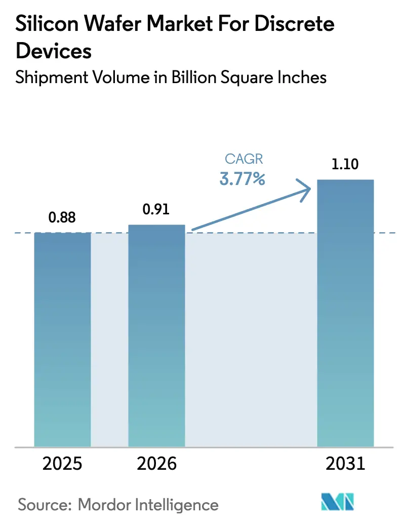
| Market Volume (2026) | 0.91 Billion Square Inches |
| Market Volume (2031) | 1.10 Billion Square Inches |
| Growth Rate (2026 - 2031) | 3.77% CAGR |
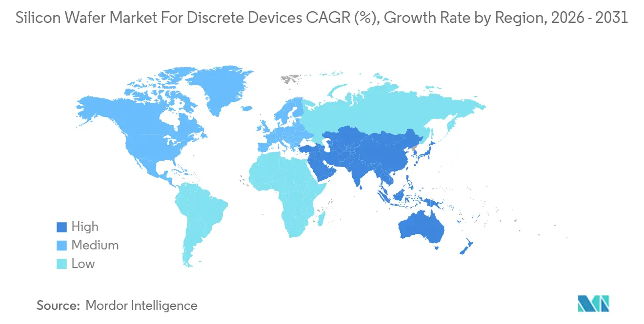
| Fastest Growing Market | Asia Pacific |
| Largest Market | Asia Pacific |
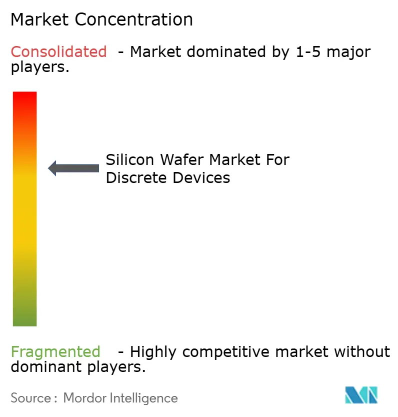
| Market Concentration | Medium |
Major Players *Disclaimer: Major Players sorted in no particular order Image © Mordor Intelligence. Reuse requires attribution under CC BY 4.0. | |
Analysis of Silicon Wafer Market For Discrete Devices by Mordor Intelligence
The silicon wafer market size for discrete devices was valued at 0.88 billion square inches in 2025 and is estimated to grow from 0.91 billion square inches in 2026 to reach 1.10 billion square inches by 2031, at a CAGR of 3.77% during the forecast period (2026-2031). Demand pivots toward power-oriented substrates as battery-electric vehicles, renewable-energy inverters, and factory-automation drives require higher current ratings than legacy consumer electronics. Government subsidies under the United States CHIPS and Science Act, the European Chips Act, and China’s third Integrated Circuit Fund are accelerating 200 millimeter line additions, compressing equipment payback periods and intensifying supplier competition. Polysilicon spot-price recovery to USD 8-9 per kilogram in early 2025 injected margin volatility, prompting wafer suppliers to embed index-based escalators in long-term contracts. Automotive electrification now anchors substrate allocation, with per-vehicle discrete content tripling to more than 1 200 units in battery-electric platforms, and industrial-motor-drive retrofits add a second structural leg to volume growth. Simultaneously, export-control regimes that restrict advanced deposition and lithography tools to China are bifurcating supply chains, extending lead times for non-Chinese buyers, and motivating multinational OEMs to dual-source wafers across regions.
Key Report Takeaways
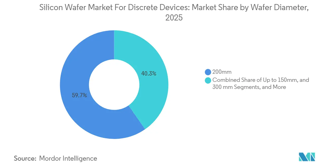
- By wafer diameter, the 200 millimeter segment held 59.66% of the silicon wafer market for discrete devices share in 2025, the 300 millimeter format is projected to expand at a 4.52% CAGR through 2031.
- By wafer type, prime polished wafers commanded 45.37% of the silicon wafer market for discrete devices size in 2025, specialty silicon substrates are forecast to rise at a 4.24% CAGR to 2031.
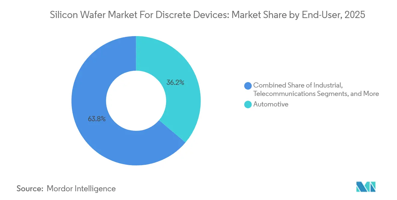
- By end-user, automotive captured 36.17% of the silicon wafer market for discrete devices share in 2025, automotive leads growth at a 4.72% CAGR between 2026 and 2031.
- By geography, Asia-Pacific dominated with 81.84% share of the silicon wafer market for discrete devices size for memory devices in 2025 and is advancing at a 4.79% CAGR through 2031.
Note: Market size and forecast figures in this report are generated using Mordor Intelligence’s proprietary estimation framework, updated with the latest available data and insights as of January 2026.
Insights and Trends of Silicon Wafer Market For Discrete Devices
Drivers Impact Analysis*
| Driver | (~) % Impact on CAGR Forecast | Geographic Relevance | Impact Timeline |
|---|---|---|---|
| Expansion of EV fast-charging infrastructure requiring high-current diodes | +1.2% | Global, concentrated in China, Europe, North America | Medium term (2–4 years) |
| Adoption of GaN/SiC hybrid modules increasing demand for high-resistivity silicon substrates | +0.9% | Global, led by Germany, Japan, United States | Medium term (2–4 years) |
| Government incentives for domestic discrete component manufacturing | +0.8% | North America, Europe, China | Long term (≥ 4 years) |
| Mature power semiconductor replacement with high-voltage discrete devices | +0.5% | Asia-Pacific core, spill-over to Middle East and Africa | Long term (≥ 4 years) |
| Rising demand for power-management ICs in IoT edge devices | +0.4% | Global, early adoption in North America, Europe | Short term (≤ 2 years) |
| Supply-chain localization mandates in automotive sector | +0.3% | Europe, North America, nascent in India | Medium term (2–4 years) |
| Source: Mordor Intelligence | |||
Expansion Of EV Fast-Charging Infrastructure Requiring High-Current Diodes
Ultra-fast chargers rated at 350 kilowatts now dominate highway corridors in China, Europe, and the United States, and each installation consumes 8-12 discrete diodes rated for 1 200-1 700 volts and more than 100 amperes.[1] International Energy Agency, “Global EV Outlook 2024,” iea.org Wolfspeed unveiled a 200 millimeter SiC-on-silicon epitaxial platform in February 2025 that targets these rectifier stages and demonstrates how wafer metrics such as bow, warp, and defect density must tighten when surge-current requirements rise. China’s State Grid added 120 000 ultra-fast chargers in 2025, translating to incremental demand for roughly 15-20 million square inches of high-current-diode substrates. The European Union’s Alternative Fuels Infrastructure Regulation mandates interoperable charging networks by 2027, locking in discrete-heavy Combined Charging System protocols. Higher switching frequencies above 50 kilohertz are shifting preference toward SiC Schottky diodes on high-resistivity silicon, a trend that lifts specialty-substrate volumes ahead of prime polished grades.
Adoption Of GaN/SiC Hybrid Modules Increasing Demand For High-Resistivity Silicon Substrates
Hybrid power modules that co-package GaN HEMTs with SiC diodes on high-resistivity silicon offer cost-per-watt metrics 30-40% below monolithic SiC, enabling automakers to meet USD 0.15 per watt system targets.[2]Infineon Technologies, “Power Semiconductors for Automotive Applications,” infineon.com Infineon’s CoolSiC devices, released in March 2024, ride this architecture and already ship on 200 millimeter wafers specified at 1 000-10 000 ohm-centimeters. STMicroelectronics reported a 28% revenue jump in hybrid modules during 2024, with 65% of units sold to automotive customers, underscoring the commercial traction of these substrates. Japan’s Ministry of Economy, Trade and Industry allocated JPY 45 billion (USD 307 million) in fiscal 2025 to subsidize domestic production of high-resistivity silicon, explicitly linking national policy to automotive power electronics. GaN on silicon for 650 volt devices requires 111 crystal orientation with threading-dislocation density under 10^6 cm-2, capabilities delivered only by specialty-wafer suppliers, reinforcing supply-chain entry barriers.
Government Incentives For Domestic Discrete Component Manufacturing
Public-capital commitments exceed USD 100 billion across the United States, European Union, and China, sharply lowering hurdle rates for new wafer fabs. GlobalWafers secured USD 400 million in CHIPS Act funding in December 2024 for a 300 millimeter facility in Texas, with 30% of future output promised to power discretes. Europe’s Important Project of Common European Interest framework cleared EUR 700 million (USD 791 million) in January 2025 for a pilot line supporting STMicroelectronics, Infineon Technologies, and onsemi. China’s Phase III Big Fund injected CNY 344 billion (USD 47.5 billion) in May 2024 to lift 200 millimeter capacity aimed at mature-node power devices. These programs shorten payback periods from 12-15 years to roughly 8 years and invite second-tier suppliers into merchant markets, pressuring incumbent price premiums.
Mature Power Semiconductor Replacement With High-Voltage Discrete Devices
More than 2 billion 600 volt IGBTs installed in industrial motor drives between 2010 and 2015 are now below new 96% efficiency thresholds in the European Union’s 2024 Ecodesign Directive. Replacement demand favors 1 200 volt devices fabricated on thinner epitaxial wafers that cut conduction losses, lifting 200 millimeter wafer orders from industrial drive OEMs. onsemi noted industrial refreshes generated 18% of discrete revenue in Q3 2024, with average selling prices 12% above new-equipment sales because buyers prioritize drop-in form factors and short qualification cycles. China’s GB/T 43234-2023 rail standard simultaneously raises on-state voltage requirements, moving traction OEMs toward higher-voltage discretes produced on 200 millimeter substrates. Wafer makers that kept legacy 200 millimeter lines active now exploit lead-time advantages of up to 24 months versus new entrants still procuring refurbished tool sets.
Restraints Impact Analysis*
| Restraint | (~) % Impact on CAGR Forecast | Geographic Relevance | Impact Timeline |
|---|---|---|---|
| Price volatility of polysilicon and energy costs | -0.8% | Global, acute in Europe | Short term (≤ 2 years) |
| Prolonged downcycles in consumer electronics affecting low-power discrete consumption | -0.6% | Asia-Pacific core, spill-over to North America | Short term (≤ 2 years) |
| Geopolitical export controls on advanced wafer manufacturing equipment | -0.4% | China with secondary global effects | Medium term (2–4 years) |
| Technical limits of silicon for ultra-high-voltage switching (> 10 kV) | -0.3% | Global, early in grid-tied and rail applications | Long term (≥ 4 years) |
| Source: Mordor Intelligence | |||
Price Volatility Of Polysilicon And Energy Costs
Polysilicon prices swung from USD 6 to USD 35 per kilogram between 2022 and 2025, and although early-2025 spot levels rebounded to USD 8-9 per kilogram, long-term contracts hover at USD 11-13, squeezing merchant wafer margins. European producers face electricity tariffs averaging EUR 0.18 per kilowatt-hour (USD 0.20 per kilowatt-hour), triple 2019 levels, and crystal growth consumes roughly 225 kilowatt-hours per kilogram of ingot, magnifying exposure. Chinese provinces offset energy intensity with subsidized industrial rates as low as CNY 0.35 per kilowatt-hour (USD 0.05), while the United States Inflation Reduction Act’s production credit refunds USD 0.03 per kilowatt-hour for clean-energy use.[3] Internal Revenue Service, “Advanced Manufacturing Production Credit,” irs.gov Supply concentration among five polysilicon vendors amplifies volatility, forcing wafer suppliers to incorporate pass-through clauses or risk negative gross margins during spikes.
Prolonged Downcycles In Consumer Electronics Affecting Low-Power Discrete Consumption
Global smartphone unit shipments fell 3.2% in 2024 and another 1.8% in 2025, and PC shipments contracted 5.1% and 2.9% over the same period, trimming wafer demand for low-power discretes embedded in power-management and protection circuits. Each smartphone contains roughly 50 discrete components, so shipment declines erased about 13 million square inches of wafer demand, equal to 1.5% of 2025 global volume. Mid-tier device makers responded by integrating formerly discrete functions into power-management ICs, while premium models retained discrete counts, leaving wafer suppliers exposed to the middle of the price pyramid. 150 millimeter wafer producers are most vulnerable because their customer base leans toward legacy consumer nodes that struggle to migrate upward into automotive or industrial sockets without full requalification.
*Our forecasts treat driver/restraint impacts as directional, not additive. The impact forecasts reflect baseline growth, mix effects, and variable interactions.
Segment Analysis
By Wafer Diameter: Format Economics Drive 200 Millimeter Dominance
The 200 millimeter slice held 59.66% of the silicon wafer market share in 2025, anchored by fully depreciated fab assets whose cost-per-die remains unbeatable for discrete transistors and diodes. Automotive-qualified fabs in Japan, Czech Republic, and Malaysia run 90%-plus utilization because this diameter balances throughput with product-mix flexibility. 300 millimeter substrates account for only 24% of the silicon wafer market size but are forecast to grow 4.52% annually through 2031 as integrated power-management ICs and multi-chip analog modules migrate to larger wafers to spread lithography overhead across hundreds of die. Texas Instruments will dedicate 40% of its Richardson Fab output to analog and power, backstopping demand for 300 millimeter supply.
The up-to-150 millimeter tier persists in niche RF-diode, thyristor, and sensor markets where exotic crystal orientations justify smaller diameters. SEMI projects 200 millimeter shipments across all semiconductor segments to decline 1.2% annually through 2028, yet discrete-device demand partially offsets this bleed by absorbing capacity vacated by memory and MCU production. Supply-chain resiliency concerns are also pushing automotive OEMs to dual-source 200 millimeter wafers from both Japan and China, creating regional hedges against seismic or geopolitical events.


By Wafer Type: Specialty Silicon Outpaces Commodity Grades
Prime polished wafers accounted for 45.37% of volume in 2025, servicing cost-sensitive consumer and telecommunications demand that tolerates surface-roughness targets of 0.2 nanometers. Specialty grades high-resistivity, power-grade, and sensor-grade expanded 19% year on year at Shin-Etsu Chemical because automotive and industrial buyers require 1 000-10 000 ohm-centimeter resistivity to mitigate switching losses in 1 200 volt MOSFETs. Specialty substrates captured 25% of the silicon wafer market size for discretes and are growing at a 4.24% CAGR, driven by GaN-on-silicon and SiC hybrid modules that need defect density below 0.3 cm-2.
Epitaxial wafers, already 25% of volume, rise 3.9% annually as Tier 1 suppliers specify dopant-profile control within ±3% across the wafer to guarantee on-resistance under 100 milliohms. Silicon-on-insulator remains niche at under 5% share, yet its average selling price is three to four times prime polished, providing margin upside for suppliers such as Soitec whose SmartSiC hybrid substrates shipped 50 000 wafers in 2024. SUMCO forecasts its product mix shifting from 55% prime polished toward 50% by 2028 as specialty grades climb to 35%, reflecting the pull of electrification.
By End-User: Automotive Electrification Reshapes Demand
Automotive held 36.17% of volume in 2025 and is poised to capture 42-45% by 2031 as battery-electric vehicle output doubles from 14 million units in 2024 to nearly 28 million by decade’s end. Each BEV consumes 1 200-1 500 discrete devices spanning traction inverters, onboard chargers, and DC-DC converters, tripling the silicon wafer market size relative to internal-combustion-engine vehicles. Industrial segments variable-speed drives, uninterruptible power supplies, and renewable-energy inverters represent 22% share and ride a replacement cycle triggered by tougher efficiency mandates and end-of-life equipment retirements. Telecommunications absorbs 12% as 48-volt rack architectures proliferate in data centers and 5G base stations.
Consumer electronics shrank to 18% share in 2025 and contracts 1.2% annually as smartphones and PCs integrate formerly discrete functions into advanced SoCs. Medical, aerospace, and defense collectively make up the remaining 12%, offering stable but low-volume demand bound by multi-year qualification cycles. The discrete wafer mix therefore skews decisively toward automotive grade over the forecast horizon, lifting traceability, zero-defect, and high-resistivity requirements throughout the supplier base.
Geography Analysis
Asia-Pacific commanded 81.84% of 2025 volume and is expected to grow at a 4.79% CAGR through 2031 as Japan, Taiwan, and China scale 200 millimeter capacity. Shin-Etsu Chemical and SUMCO shipped more than 450 million square inches combined in 2024, leveraging proprietary Czochralski techniques for resistivity uniformity within ±5%. Taiwan’s GlobalWafers dedicated 35% of 2024 output to discrete customers, using long-term contracts with onsemi and Vishay to run utilization above 85%. Chinese suppliers NSIG and Zhonghuan added 80 million square inches of 200 millimeter capacity during 2024-2025, bolstered by CNY 8 billion (USD 1.1 billion) in provincial subsidies.
North America accounted for 8% in 2025. CHIPS Act funding of USD 400 million is underwriting GlobalWafers’ new Texas fab that will reserve 40% of its 300 millimeter output for power discretes starting 2027.[4]U.S. Department of Commerce, “Biden-Harris Administration Announces $400 Million for GlobalWafers,” commerce.gov Hemlock Semiconductor’s USD 325 million polysilicon expansion in Michigan further localizes upstream supply and insulates U.S. wafer lines from Chinese feedstock risk, though ramp will not complete until 2029.
Europe held 6% of output, with Siltronic AG and Soitec serving automotive hubs in Germany and France via epitaxial and SOI lines. Important Project of Common European Interest approval enabled EUR 700 million (USD 791 million) for a power-discrete pilot line supporting STMicroelectronics, Infineon, and onsemi, but commercial production is unlikely before 2028. South America and the Middle East and Africa combined for less than 5%, relying on imported wafers for assembly and test facilities.
The heavy concentration of substrate production within 100 kilometers of Taiwan’s west coast exposes the silicon wafer market to earthquake and geopolitical disruptions. Automotive OEMs increasingly mandate dual-regional sourcing, pairing Japanese or Taiwanese supply with backup capacity in the United States or Europe to mitigate single-point-of-failure risk.

Competitive Landscape
The top five merchant suppliers, Shin-Etsu Chemical, SUMCO Corporation, GlobalWafers, Siltronic AG, and SK Siltron, controlled a major share of volume in 2025, indicating moderate concentration. Shin-Etsu leads with about a 28% share, leveraging captive polysilicon, patented melt-purification, and vertical integration that lower defect density to 0.05 cm-2 on 200-millimeter wafers. SUMCO follows at 20%, anchoring share through multi-year automotive contracts that fix prices yet guarantee a minimum offtake, cushioning demand shocks.
Chinese challengers such as NSIG and Hangzhou Semiconductor Wafer undercut spot pricing by up to 20% to penetrate consumer and telecom segments that tolerate wider process tolerances. Specialty innovators create white-space opportunities: Soitec’s SmartSiC hybrid substrate booked three European automotive Tier 1 design wins in 2025; Siltronic’s magnetic Czochralski technique reduces oxygen precipitation by 40%, enabling thinner epitaxial layers.
Consolidation remains unlikely because zero-defect automotive qualification requirements lock in long-term relationships and discourage quick customer migration.
Leaders of Silicon Wafer Market For Discrete Devices
Shin-Etsu Chemical Co Ltd
SUMCO Corporation
GlobalWafers Co Ltd
Siltronic AG
SK siltron Co Ltd
- *Disclaimer: Major Players sorted in no particular order

Recent Industry Developments
- February 2026: Shin-Etsu Chemical announced a JPY 120 billion (USD 820 million) plan to lift 200 millimeter epitaxial capacity in Takasaki by 25% with completion slated for Q2 2028.
- January 2026: GlobalWafers signed a 10-year, USD 2 billion supply agreement with onsemi covering 40 million square inches annually of 200 millimeter prime polished and epitaxial wafers.
- December 2025: SUMCO Corporation finished a USD 450 million expansion of its Imari fab, adding 35 million square inches of 200 millimeter high-resistivity capacity and attaining ISO 26262 certification.
- October 2025: Soitec and STMicroelectronics entered a joint-development pact to optimize SmartSiC substrates for 800 volt traction inverters, with pilot output expected in Q3 2026.


Scope of Report on Silicon Wafer Market For Discrete Devices
The global silicon wafer market for discrete devices is witnessing significant growth due to increasing demand across various end-user industries. Factors such as advancements in semiconductor technology, rising adoption of consumer electronics, and the growing need for efficient power management solutions are driving the market. Additionally, the automotive sector's shift toward electric vehicles and autonomous driving technologies is further propelling the demand for silicon wafers.
The Global Silicon Wafer Market for Discrete Devices Report is Segmented by Wafer Diameter (Up to 150mm, 200mm, 300mm), Wafer Type (Prime Polished, Epitaxial, Silicon-on-Insulator, Specialty Silicon), End-user (Consumer Electronics, Industrial, Telecommunications, Automotive, Other End-user Applications), and Geography (North America, Europe, Asia-Pacific, South America, Middle East and Africa). The Market Forecasts are Provided in Terms of Volume (Square Inches).
| Up to 150mm |
| 200 mm |
| 300 mm |
| Prime Polished |
| Epitaxial |
| Silicon-on-Insulator (SOI) |
| Specialty Silicon (High-Resistivity, Power, Sensor-Grade) |
| Consumer Electronics | Mobile and Smartphones |
| PCs and Servers | |
| Industrial | |
| Telecommunications | |
| Automotive | |
| Other End-user Applications |
| North America | United States |
| Canada | |
| Mexico | |
| Europe | Germany |
| United Kingdom | |
| France | |
| Rest of Europe | |
| Asia-Pacific | China |
| Japan | |
| India | |
| South Korea | |
| Taiwan | |
| Rest of Asia-Pacific | |
| South America | |
| Middle East and Africa |
| By Wafer Diameter | Up to 150mm | |
| 200 mm | ||
| 300 mm | ||
| By Wafer Type | Prime Polished | |
| Epitaxial | ||
| Silicon-on-Insulator (SOI) | ||
| Specialty Silicon (High-Resistivity, Power, Sensor-Grade) | ||
| By End-user | Consumer Electronics | Mobile and Smartphones |
| PCs and Servers | ||
| Industrial | ||
| Telecommunications | ||
| Automotive | ||
| Other End-user Applications | ||
| By Geography | North America | United States |
| Canada | ||
| Mexico | ||
| Europe | Germany | |
| United Kingdom | ||
| France | ||
| Rest of Europe | ||
| Asia-Pacific | China | |
| Japan | ||
| India | ||
| South Korea | ||
| Taiwan | ||
| Rest of Asia-Pacific | ||
| South America | ||
| Middle East and Africa | ||


Key Questions Answered in the Report
How large will global demand for silicon wafers used in discrete devices be by 2031?
The market is projected to reach 1.10 billion square inches by 2031, expanding at a 3.77% CAGR from 2026 to 2031.
What proportion of wafer volume is expected to come from automotive applications by the end of the decade?
Automotive consumption is forecast to rise from 36.17% in 2025 to roughly 42-45% of total volume by 2031.
Which wafer diameter format presently anchors discrete-device production?
200 millimeter substrates dominate with 59.66% share in 2025 and retain cost-of-ownership advantages for low-complexity transistors and diodes.
How are national subsidy programs shaping new capacity additions?
Funding from the United States CHIPS Act, the European Chips Act, and China’s Big Fund has cut payback periods to about eight years, spurring both 200 millimeter and 300 millimeter greenfield fabs.
Why is demand for high-resistivity specialty silicon growing faster than prime polished grades?
GaN/SiC hybrid power modules and 350 kilowatt EV chargers need resistivity of 1 000-10 000 ohm-cm to curb switching losses, lifting specialty-substrate shipments at a 4.24% CAGR.
What is the chief supply-chain risk linked to geographic concentration?
About 22% of global wafer output sits within 100 kilometers of the Taiwan Strait, exposing buyers to simultaneous earthquake and geopolitical disruption.
Page last updated on:


