United States Semiconductor Silicon Wafer Market Size and Share
Market Overview
| Study Period | 2020 - 2031 |
|---|---|
| Forecast Data Period | 2026 - 2031 |
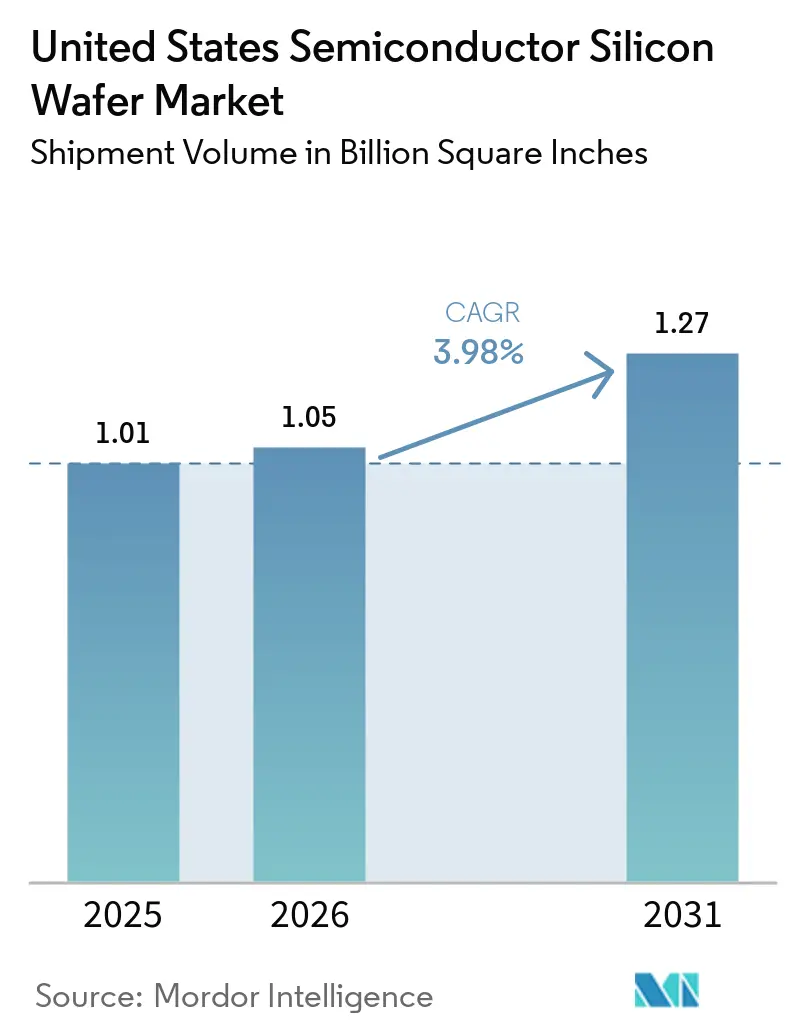
| Base Year Market Size (2025) | 1.01 Billion Square Inches |
| Market Volume (2026) | 1.05 Billion Square Inches |
| Market Volume (2031) | 1.27 Billion Square Inches |
| Growth Rate (2026 - 2031) | 3.98% CAGR |
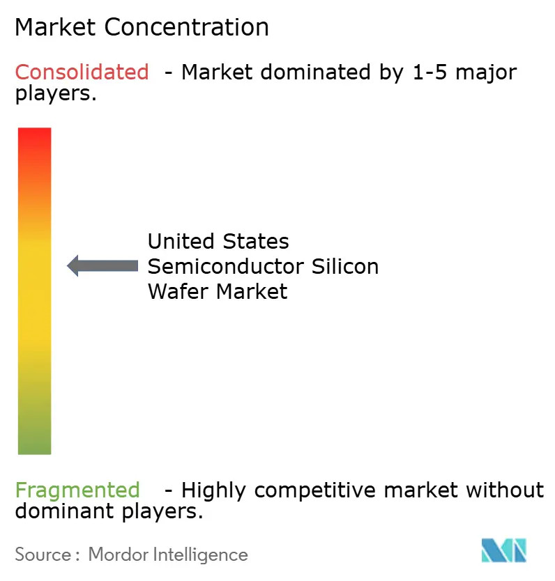
| Market Concentration | Medium |
Major Players *Disclaimer: Major Players sorted in no particular order Image © Mordor Intelligence. Reuse requires attribution under CC BY 4.0. | |
United States Semiconductor Silicon Wafer Market Analysis by Mordor Intelligence
The United States Semiconductor Silicon Wafer Market size in terms of shipment volume is projected to be 1.01 Billion Square Inches in 2025, 1.05 Billion Square Inches in 2026, and reach 1.27 Billion Square Inches by 2031, growing at a CAGR of 3.98% from 2026 to 2031. Federal industrial policy rather than short product cycles now shapes capacity plans, and incentives from the CHIPS and Science Act have already unlocked more than USD 30 billion in direct funding plus USD 5.5 billion in loans for new fabs. Leading-edge logic demand for 4 nanometer to 2 nanometer nodes is expanding local substrate requirements, while automotive electrification, industrial automation, and data-center artificial intelligence together sustain mature-node consumption. Supply, however, has not caught up; large-diameter 300 millimeter wafers are scaling faster than 200 millimeter formats, and domestic polysilicon output remains limited, leaving import exposure in the near term. Equipment makers are tightening flatness and defect controls for gate-all-around transistors, and those stricter specifications are raising both substrate cost and qualification time.
Key Report Takeaways
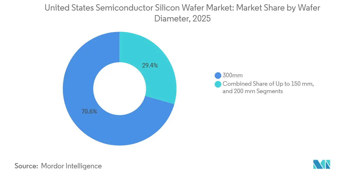
- By wafer diameter, 300 millimeter substrates led with 70.62% of the United States semiconductor silicon wafer market share in 2025.
- By semiconductor device type, logic accounted for 33.09% of the United States semiconductor silicon wafer market size in 2025 and is projected to expand at a 5.25% CAGR through 2031.
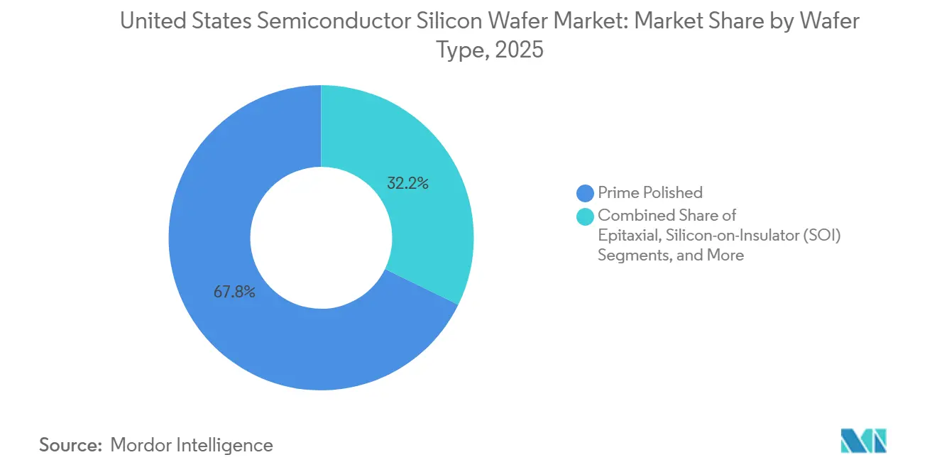
- By wafer type, prime polished wafers held a 67.77% share in 2025, whereas silicon-on-insulator substrates are advancing at a 4.86% CAGR to 2031.
- By end-user, consumer electronics represented 37.55% of volume in 2025, while automotive uses are forecast to grow at a 4.72% CAGR through 2031.
Note: Market size and forecast figures in this report are generated using Mordor Intelligence’s proprietary estimation framework, updated with the latest available data and insights as of January 2026.
Future direction is shaped by developments occurring across multiple countries and regions, with United states contributing to the overall trajectory. The outlook on worldwide semiconductor silicon wafer market reflects how these are expected to evolve collectively.
United States Semiconductor Silicon Wafer Market Trends and Insights
Drivers Impact Analysis*
| Driver | (~) % Impact on CAGR Forecast | Geographic Relevance | Impact Timeline |
|---|---|---|---|
| Capacity Expansions by Leading Foundries | +1.5% | Arizona, Ohio, Texas, New York | Medium term (2-4 years) |
| Surge in U.S. CHIPS Act Incentives | +1.2% | Nationwide with early gains in Arizona, Ohio, New York | Short term (≤ 2 years) |
| Transition Toward 300 mm Wafers in Logic | +0.8% | Nationwide with spillover to packaging hubs | Long term (≥ 4 years) |
| Rising Demand for Si Power Devices in EVs | +0.6% | Michigan, California, Texas automotive corridors | Medium term (2-4 years) |
| AI-Optimized SOI Wafer Demand | +0.4% | Data-center and edge-computing clusters | Short term (≤ 2 years) |
| Defense-Grade Radiation-Hard Silicon | +0.2% | Defense contractors in Massachusetts, California, Virginia | Long term (≥ 4 years) |
| Source: Mordor Intelligence | |||
Capacity Expansions by Leading Foundries
Unprecedented capital spending by three global leaders is reshaping the United States semiconductor silicon wafer market. TSMC is installing six mega-fabs and two advanced packaging lines in Arizona, Intel is adding new 18A lines across four states, and Samsung is scaling a two-nanometer logic campus in Texas. Each site will consume millions of 300 millimeter wafers every year once fully qualified. Domestic substrate makers are racing to match that pull, but new crystal-growth and slicing workshops will not reach steady output until 2027, which leaves a two-year window in which foundries remain tied to imports.[1]U.S. Department of Commerce, “Biden-Harris Administration Announces CHIPS Incentives Award for TSMC Arizona,” commerce.gov
Surge in U.S. CHIPS Act Incentives
The CHIPS and Science Act lowers the hurdle rate for new plants and has already redirected investments that might have gone to Asia. Matching grants cut the effective cost of a United States wafer line by as much as a fifth and include hard guardrails that block advanced-node expansion in China for a decade. Those terms keep incremental demand local, yet raw polysilicon still arrives from Germany or Japan, meaning supply security is only partially solved.
Transition Toward 300 mm Wafers in Logic Nodes
Gate-all-around transistors, backside power delivery, and chiplet packaging all depend on wide-diameter substrates that support higher die counts. As a result, 300 millimeter volume in the United States semiconductor silicon wafer market is growing almost two percentage points faster than the overall market, while 200 millimeter lines remain essential for analog and power parts. This divergence is forcing suppliers to split capital between the two paths and is widening delivery-time gaps for automotive customers.[2]SEMI, “SEMI Reports 2025 Global Silicon Wafer Shipments Up 5.8 Percent to 12,973 Million Square Inches,” semi.org
Rising Demand for Si Power Devices in EVs
Electric vehicles require two to three times the silicon area of traditional cars, largely in 200 millimeter wafers that house power switches. Although wide-bandgap substitutes are gaining, silicon still dominates 400 volt platforms and remains price-competitive. U.S. wafer plants near Michigan assembly hubs have begun to dedicate high-resistivity lines to traction inverters, yet supply remains thin until new 200 millimeter projects finish ramping.
Restraints Impact Analysis*
| Restraint | (~) % Impact on CAGR Forecast | Geographic Relevance | Impact Timeline |
|---|---|---|---|
| Cyclical Memory Downturns | -0.7% | Idaho, Virginia, linked DRAM and NAND clusters | Short term (≤ 2 years) |
| Supply Chain Geographic Concentration Risk | -0.5% | Dependence on East Asian polysilicon and ingot imports | Medium term (2-4 years) |
| Crystalline Defect Limits at 3 nm and Below | -0.3% | Leading-edge logic fabs | Long term (≥ 4 years) |
| Growing Competition from SiC and GaN | -0.4% | Automotive and industrial power segments | Medium term (2-4 years) |
| Source: Mordor Intelligence | |||
Cyclical Memory Downturns
DRAM and NAND suppliers cut orders sharply in early 2025 as smartphone sales softened and cloud firms digested inventory. Memory wafers represent nearly one-quarter of the United States semiconductor silicon wafer market, so a single price correction quickly deflates substrate revenue. High-bandwidth memory stays healthy for artificial intelligence servers, but that niche is too small to stabilize overall demand.[3]Micron Technology, “Micron Investor Relations News Releases,” micron.com
Supply Chain Geographic Concentration Risk
Less than one-tenth of semiconductor-grade polysilicon is produced on U.S. soil, and most ingot pulling still takes place in Japan and Taiwan. Shipping delays across the Pacific can stretch to two months, well beyond just-in-time buffers at new Arizona and Ohio fabs. Recent federal awards for a Missouri crystal-growth plant ease the constraint only after 2027.
*Our forecasts treat driver/restraint impacts as directional, not additive. The impact forecasts reflect baseline growth, mix effects, and variable interactions.
Segment Analysis
By Wafer Diameter: 300 mm Dominance Masks 200 mm Bottleneck
The 300 millimeter slice of the United States semiconductor silicon wafer market size reached 70.62% of volume in 2025 and is forecast to rise at a 4.95% CAGR to 2031. TSMC’s and Intel’s new Arizona and Ohio fabs alone will add more than 30 million square inches of demand once fully loaded. High die counts per wafer improve cost efficiency, yet only three global suppliers hold a meaningful share of 300 millimeter crystal capacity.
By contrast, 200 millimeter substrates underpin analog, MEMS, and automotive power electronics. That format expanded 14% between 2023 and 2026, but U.S. capacity equals only 14% of global supply. Automakers face a possible shortfall in 2026-2027, when inverter chips will compete with industrial controls for the same wafers. Sub-150 millimeter formats persist in defense and legacy lines but advance just 1.8% a year, reinforcing a three-speed supply picture in which wafer makers must focus investment where volume and margin justify.


By Semiconductor Device Type: Logic Surges, Memory Stalls
Logic captured 33.09% of United States semiconductor silicon wafer market share in 2025 and is tracking a 5.25% CAGR through 2031, propelled by artificial intelligence accelerators that need leading-edge nodes and epitaxial layers. TSMC disclosed that three-nanometer revenue overtook smartphones in late 2025, confirming the momentum behind high-performance computing.
Memory volumes, however, dipped in early 2025 as DRAM and NAND prices softened. Although HBM devices for training clusters stay profitable, they occupy less than 5% of memory wafer volume. Analog and discrete components show steady 3-4% growth in 200 millimeter fabs, while sensors and MEMS stand near the same pace, helped by automotive radar and smart speakers.
By Wafer Type: SOI Gains as Prime Polished Plateaus
Prime polished substrates held 67.77% of United States semiconductor silicon wafer market size in 2025 yet advance at only 3.7% a year because customers are moving selected products to epitaxial or SOI formats. Polished wafers remain the workhorse for mainstream logic and memory, but their share slides slowly as node shrinks impose tighter electrical isolation needs.
Silicon-on-insulator wafers post the fastest rise at 4.86% CAGR, powered by edge artificial intelligence chips and co-packaged optics. Epitaxial layers follow closely for gate-all-around processes that require precise doping and ultra-low defect counts. Specialty silicon, including ultra-high-resistivity float-zone material, answers discrete power applications in electric vehicles and renewable inverters but commands smaller volumes.
By End-User: Automotive Fastest, Consumer Electronics Largest
Consumer electronics still use 37.55% of United States semiconductor silicon wafer market volume, yet the mix is tilting from smartphones toward data-center accelerators that each consume two to three times the silicon area of a handset processor. Artificial intelligence servers therefore generate more revenue per wafer.
Automotive applications lead growth at a projected 4.72% CAGR to 2031. Silicon IGBTs and MOSFETs for traction and charging run mainly on 200 millimeter wafers today. While silicon carbide and gallium nitride are winning high-voltage sockets, silicon remains the economical choice for 400 volt platforms and for discrete low-voltage converters. Industrial, telecom, and defense segments together provide a steady base that cushions cyclic swings in consumer demand.
Geography Analysis
Most volume clusters in four states, creating dense corridors of demand and logistics efficiency. Arizona hosts six TSMC fabs and Intel’s Ocotillo complex, together projected to absorb more than 20 million square inches of 300 millimeter supply each year by decade-end. Ohio’s Licking County campus adds two Intel mega-fabs plus a packaging plant and enjoys state workforce grants that speed ramp schedules. Texas links Samsung’s Taylor logic line with analog and power houses such as Texas Instruments and Infineon, ensuring mixed wafer demand across diameters. New York’s Albany NanoTech center serves as a pilot hub where process flows qualify before high-volume transfer.
A layered stack of federal and state incentives can trim delivered wafer cost by up to 20 percent versus Asia, yet raw polysilicon and many ingots still cross the Pacific or Atlantic. GlobalWafers is expanding a Missouri plant funded by USD 406 million in CHIPS Act grants, but its material will draw feedstock from Germany and Japan until domestic melt shops appear. Smaller providers in Virginia, Oregon, and California cater mostly to defense or research clients, leaving mainstream foundries reliant on imports until at least 2027.
Concentrated geography brings both efficiency and vulnerability. Natural disasters, labor disputes, or infrastructure outages in any one of the four core states would ripple quickly through downstream assembly lines. As insurance, a handful of suppliers are placing satellite reclaim and test-wafer facilities in Colorado and Utah to diversify inventory buffers.
Analysis of the semiconductor silicon wafer market by Mordor Intelligence spans multiple other regional evaluations across Europe, North America, and Asia, supported by country-level insights for Germany, China, South Korea, Taiwan, Japan, and India, wherein local market conditions keep varying from one country to another.
Competitive Landscape
Market power is uneven. Five global suppliers control around 70 percent of 300 millimeter prime polished capacity, but specialty niches such as SOI, epitaxial, and float-zone remain far more fragmented. Shin-Etsu and SUMCO leverage vertical integration and strong balance sheets to pre-buy crystal pullers and polishing tools before demand spikes. GlobalWafers uses proximity, investing in Missouri to place finished wafers within a one-day truck haul of Arizona and Texas fabs.
Niche firms prosper by owning proprietary process steps. Soitec’s layer-transfer technology enables sub-50 nanometer SOI stacks for co-packaged optics, commanding premiums that protect margins even in down cycles. Okmetic and Virginia Semiconductor win orders for radiation-hardened substrata that meet strict military standards. Emerging challenger Qromis promotes cost-cut SOI bonding that could shave 30 percent from total wafer expense, appealing to data-center customers who weigh dollar per gigabit of I/O.
Technology race dynamics focus on epi reactors and metrology. Applied Materials and ASM International ship tools capable of sub-nanometer flatness, an essential feature for gate-all-around geometries. KLA’s inspection systems then certify defect densities below 0.1 per square centimeter, a bar that only four merchants currently meet. Federal subsidies skew competition toward plants on U.S. soil, yet upstream commodity economics push polysilicon makers to stagnate unless parallel grants appear.
United States Semiconductor Silicon Wafer Industry Leaders
Shin-Etsu Chemical Co., Ltd.
SUMCO Corporation
GlobalWafers Co., Ltd.
Siltronic AG
SK siltron Co., Ltd.
- *Disclaimer: Major Players sorted in no particular order

Recent Industry Developments
- March 2026: TSMC initiated two-nanometer wafer production at its first Arizona fab, marking the first U.S. output below three nanometers and drawing on mixed imports and emerging domestic supply.
- January 2026: Intel closed USD 7.86 billion in CHIPS Act funding plus USD 8.9 billion in equity to expand Arizona, New Mexico, Ohio, and Oregon sites, locking in 18A capacity for internal and foundry clients.
- December 2025: GlobalWafers secured USD 406 million in federal incentives for its Sherman, Texas project, scheduled to add fresh 300 millimeter output by late 2027.
- November 2025: Wacker Chemie finished a line in Germany after a EUR 300 million (USD 339 million) spend that lifts semiconductor-grade polysilicon capacity 50 percent.


United States Semiconductor Silicon Wafer Market Report Scope
The United States semiconductor silicon wafer market is a critical component of the global semiconductor industry, driven by advancements in technology and increasing demand across various applications. The market's growth is influenced by factors such as the rising adoption of consumer electronics, the expansion of 5G networks, and the growing integration of semiconductors in automotive and industrial sectors.
The United States Semiconductor Silicon Wafer Market Report is Segmented by Wafer Diameter (Up to 150mm, 200mm, 300mm), Semiconductor Device Type (Logic, Memory, Analog, Discrete, Other), Wafer Type (Prime Polished, Epitaxial, SOI, Specialty Silicon), and End-user (Consumer Electronics with Mobile and PCs subsegments, Industrial, Telecommunications, Automotive, Other). The Market Forecasts are Provided in Terms of Volume (Square Inches).
| Up to 150 mm |
| 200 mm |
| 300 mm |
| Logic |
| Memory |
| Analog |
| Discrete |
| Other Semiconductor Device Types (Optoelectronics, Sensors, Micro) |
| Prime Polished |
| Epitaxial |
| Silicon-on-Insulator (SOI) |
| Specialty Silicon (High-Resistivity, Power, Sensor-Grade) |
| Consumer Electronics | Mobile and Smartphones |
| PCs and Servers | |
| Industrial | |
| Telecommunications | |
| Automotive | |
| Other End-user |
| By Wafer Diameter | Up to 150 mm | |
| 200 mm | ||
| 300 mm | ||
| By Semiconductor Device Type | Logic | |
| Memory | ||
| Analog | ||
| Discrete | ||
| Other Semiconductor Device Types (Optoelectronics, Sensors, Micro) | ||
| By Wafer Type | Prime Polished | |
| Epitaxial | ||
| Silicon-on-Insulator (SOI) | ||
| Specialty Silicon (High-Resistivity, Power, Sensor-Grade) | ||
| By End-user | Consumer Electronics | Mobile and Smartphones |
| PCs and Servers | ||
| Industrial | ||
| Telecommunications | ||
| Automotive | ||
| Other End-user | ||


Key Questions Answered in the Report
How fast is wafer volume in the United States semiconductor silicon wafer market expected to grow?
Volume is forecast to rise from 1.05 billion square inches in 2026 to 1.27 billion square inches by 2031, a 3.98% CAGR.
Which wafer diameter represents the largest share of demand?
300 millimeter substrates led with 70.62% of total volume in 2025 and will keep expanding fastest through 2031.
What end-user sector is growing quickest?
Automotive uses are projected to increase at a 4.72% CAGR as electric vehicles add power-device content.
Why are SOI wafers gaining ground?
Silicon-on-insulator technology improves power efficiency for edge artificial intelligence and photonics, driving a 4.86% CAGR through 2031.
What risks could slow market growth?
Cyclical memory downturns and heavy reliance on imported polysilicon may trim overall CAGR by over one percentage point.
When will new domestic wafer capacity meaningfully reduce import dependence?
Plants funded under the CHIPS Act are scheduled to reach stable high-volume output between late 2027 and 2028.
Page last updated on:


