North America Semiconductor Silicon Wafer Market Size and Share
Market Overview
| Study Period | 2020 - 2031 |
|---|---|
| Forecast Data Period | 2026 - 2031 |
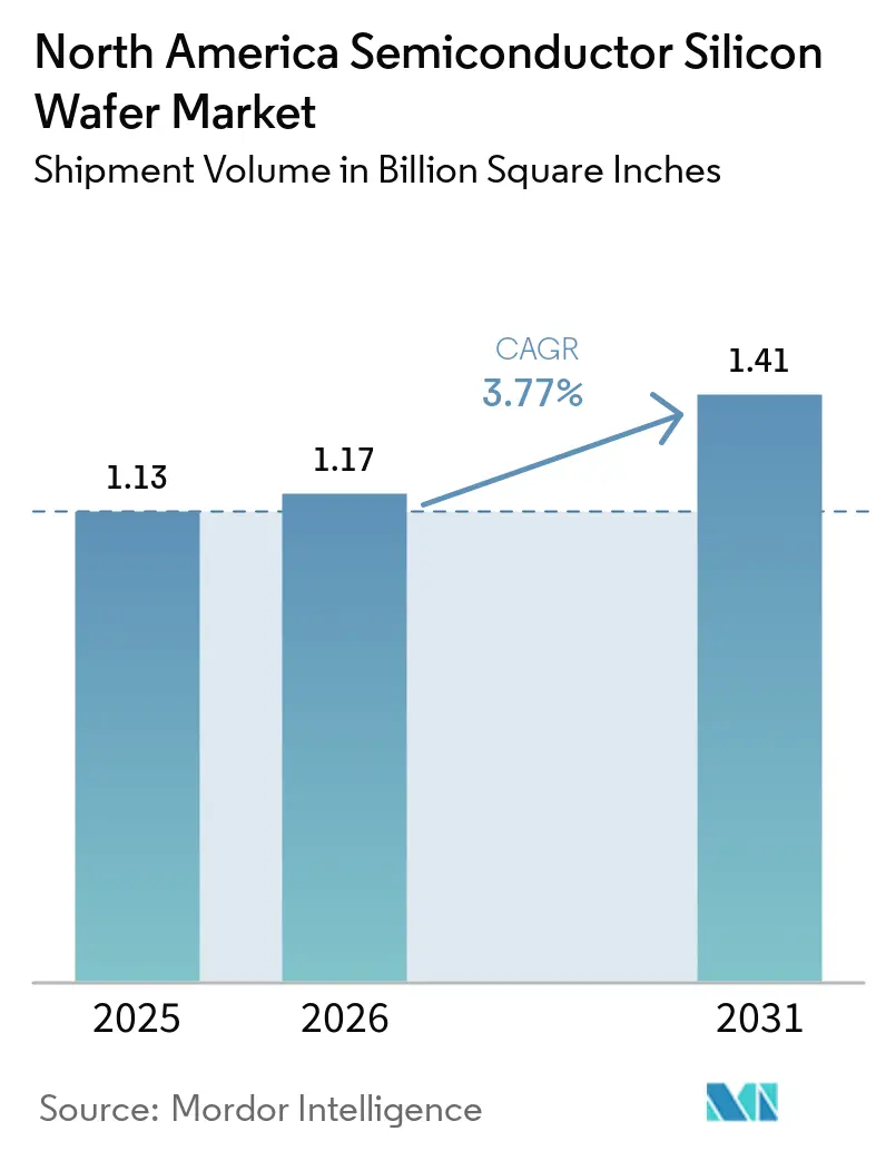
| Base Year Market Size (2025) | 1.13 Billion Square Inches |
| Market Volume (2026) | 1.17 Billion Square Inches |
| Market Volume (2031) | 1.41 Billion Square Inches |
| Growth Rate (2026 - 2031) | 3.77% CAGR |
| Market Concentration | Medium |
Major Players *Disclaimer: Major Players sorted in no particular order Image © Mordor Intelligence. Reuse requires attribution under CC BY 4.0. | |
North America Semiconductor Silicon Wafer Market Analysis by Mordor Intelligence
The North America Semiconductor Silicon Wafer Market size in terms of shipment volume is expected to grow from 1.13 Billion Square Inches in 2025 to 1.17 Billion Square Inches in 2026 and is forecast to reach 1.41 Billion Square Inches by 2031 at a 3.77% CAGR over 2026-2031. Strong U.S. industrial policy, accelerated node migration, and a synchronized build-out of 300 mm capacity underpin this trajectory. Federal CHIPS Act incentives derisk multibillion-dollar fab projects, while logic, AI accelerators, and power electronics expand wafer demand. Suppliers benefit from long-term contracts with prepayments that stabilize revenues, yet they must navigate cyclicality in memory, labor shortages, and energy bottlenecks. Localized 300 mm supply in Texas reduces tariff exposure, but dependence on imported polysilicon and process equipment persists.
Key Report Takeaways
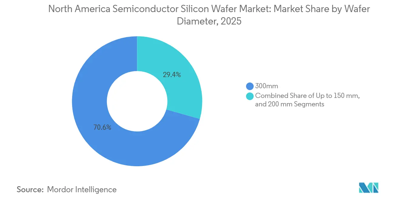
- By wafer diameter, the 300 mm segment led with 70.62% volume share in 2025 and is expanding at a 4.95% CAGR through 2031.
- By semiconductor device type, logic devices accounted for 33.09% of the North America semiconductor silicon wafer market share in 2025 and are advancing at a 5.25% CAGR to 2031.
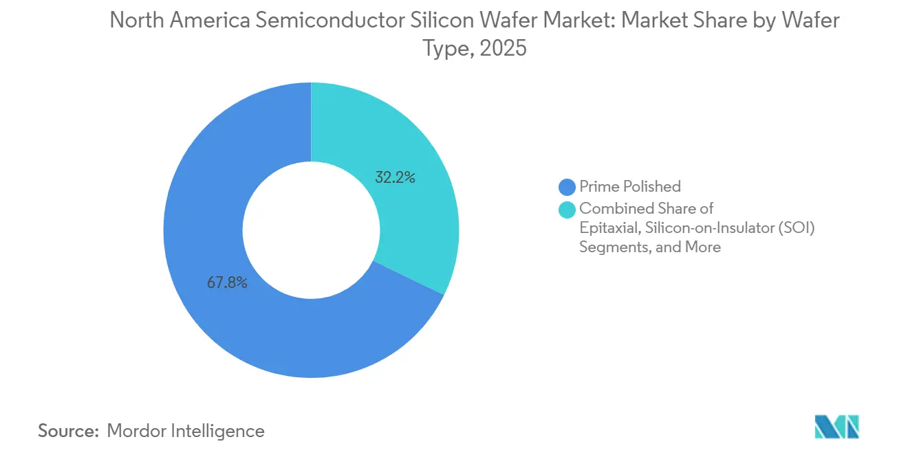
- By wafer type, prime polished substrates dominated with 67.77% volume in 2025, while silicon-on-insulator wafers are the fastest growing at a 4.86% CAGR through 2031.
- By end-user, consumer electronics held 37.55% of the North America semiconductor silicon wafer market size in 2025; automotive applications are forecast to grow at a 4.72% CAGR between 2026 and 2031.
- By geography, the United States captured 86.37% of regional wafer demand in 2025 and will mirror the overall 3.98% CAGR through 2031.
Note: Market size and forecast figures in this report are generated using Mordor Intelligence’s proprietary estimation framework, updated with the latest available data and insights as of January 2026.
Competitive positioning in North america includes both locally based firms and those operating across multiple regions. The market landscape in the global semiconductor silicon wafer industry research shows how these players are arranged internationally.
North America Semiconductor Silicon Wafer Market Trends and Insights
Drivers Impact Analysis*
| Driver | (~) % Impact on CAGR Forecast | Geographic Relevance | Impact Timeline |
|---|---|---|---|
| Capacity Expansions by Leading Foundries | +1.2% | Arizona, Texas, New York, Idaho | Medium term (2–4 years) |
| Surge in U.S. CHIPS Act Incentives | +1.0% | National, concentrated in Arizona, New York, Texas | Medium term (2–4 years) |
| Transition Toward 300 mm Wafers in Logic Nodes | +0.9% | Arizona, Texas, Oregon | Long term (≥ 4 years) |
| Rising Demand for Si Power Devices in EVs | +0.6% | North America, automotive hubs | Medium term (2–4 years) |
| AI-Optimized SOI Wafer Demand | +0.4% | National, data-center clusters | Short term (≤ 2 years) |
| Defense-Grade Radiation-Hard Silicon | +0.2% | National, defense ecosystems | Long term (≥ 4 years) |
| Source: Mordor Intelligence | |||
Capacity Expansions by Leading Foundries
Massive multiyear investments from TSMC, Intel, and Texas Instruments continue to upgrade the North America semiconductor silicon wafer market. The Arizona gigafab cluster already matches Taiwan yield levels, Intel’s Fab 52 has entered high-volume production on 18A, and Texas Instruments has automated its Sherman complex with humanoid robots. Concentrated orders allow substrate suppliers to amortize qualification costs and lock in advance payments, ensuring predictable throughput and quicker node ramps.
Surge in U.S. CHIPS Act Incentives
Direct grants, low-cost loans, and a 25% tax credit lower capital hurdles for every tier of the value chain, from polysilicon to finished wafers.[1]U.S. Department of Commerce, “Department of Commerce awards CHIPS incentives to Micron,” commerce.gov Milestone-based disbursements prevent speculative overbuilding, while clawback clauses protect taxpayers. Wafer makers leverage these subsidies to co-locate with fabs, shortening logistics cycles and enhancing supply resilience for the North America semiconductor silicon wafer market.
Transition Toward 300 mm Wafers in Logic Nodes
Advanced logic and mixed-signal products migrate to 300 mm to capture cost-per-die benefits. Foundries in Arizona and Texas integrate smart-factory analytics that push yields past 90%, reinforcing demand for defect-free 300 mm blanks.[2]SEMI, “300 mm Fab Outlook Report,” semi.org Suppliers, however, must maintain 200 mm lines for automotive and analog devices, increasing fixed-asset intensity while serving a bifurcated demand base.
Rising Demand for Si Power Devices in EVs
EV traction inverters, onboard chargers, and ADAS modules consume growing volumes of 200 mm and 300 mm silicon power wafers despite silicon carbide gains. Automakers favor silicon for auxiliary converters and battery management units where cost trumps ultimate efficiency. The surge stabilizes backend loading for suppliers during logic or memory slowdowns, enhancing overall health of the North America semiconductor silicon wafer industry.
Restraints Impact Analysis*
| Restraint | (~) % Impact on CAGR Forecast | Geographic Relevance | Impact Timeline |
|---|---|---|---|
| Cyclical Memory Downturns | -0.8% | Memory fab regions | Short term (≤ 2 years) |
| Supply Chain Geographic Concentration Risk | -0.5% | National, all fabs | Medium term (2–4 years) |
| Crystalline Defect Limits at 3 nm and Below | -0.3% | Leading-edge logic fabs | Long term (≥ 4 years) |
| Growing Competition from SiC and GaN Substrates | -0.4% | Automotive and power hubs | Medium term (2–4 years) |
| Source: Mordor Intelligence | |||
Cyclical Memory Downturns
A persistent inventory overhang in commodity DRAM and NAND used up cleanroom space without proportional wafer pull-through in 2025. Price erosion outside long-term contracts cut margins for wafer suppliers, exposing the North America semiconductor silicon wafer market to sharp quarterly swings. Although high-bandwidth memory for AI helps, it cannot fully neutralize volume softness until inventories normalize.
Supply Chain Geographic Concentration Risk
Polysilicon, quartz crucibles, and many specialty gases still arrive from Asia or Europe. Any geopolitical disruption could leave domestic fabs scrambling, especially because GlobalWafers operates the only advanced 300 mm plant inside U.S. borders. Upstream diversification projects are under way but will take years to balance the sourcing map.
*Our forecasts treat driver/restraint impacts as directional, not additive. The impact forecasts reflect baseline growth, mix effects, and variable interactions.
Segment Analysis
By Wafer Diameter: 300 mm Capacity Surges
The 300 mm slice of the North America semiconductor silicon wafer market stands at 70.62% volume and gains from leading-edge AI and 3 nm logic ramps, and expanding at a 4.95% CAGR through 2031. Large-die GPUs, high-density DRAM, and highly automated analog lines benefit from a larger surface, spreading lithography cost over more die and lifting gross margins. The North America semiconductor silicon wafer market size attached to 300 mm fabs therefore rises faster than the overall curve, reinforcing demand visibility for suppliers.
200 mm wafers remain crucial for automotive, power, and mature analog, particularly as EV content skyrockets. Capacity additions in onsemi and Infineon lines keep legacy fabs busy, preventing sudden obsolescence. Suppliers juggling both diameters offset demand cliffs and deepen relationships across device generations, which strengthens the North America semiconductor silicon wafer market over the long term.


By Semiconductor Device Type: Logic Growth Outpaces Memory
Logic devices held 33.09% of the 2025 volume and are advancing at a 5.25% CAGR to 2031, as AI inference shifts to smartphones, PCs, and edge servers. RibbonFET and backside power delivery sharpen transistor efficiency, but they also raise crystal quality demands. Wafer makers shipping to these nodes capture price premiums, lifting the North America semiconductor silicon wafer market share tied to logic.
Memory’s cyclicality tempers its net contribution despite U.S. DRAM megafab announcements. High-bandwidth memory stacks use more silicon per package, yet soft PC and handset demand restrains overall wafer lifts. Analog and discrete devices post steady, mid-single-digit volume growth, balancing the portfolio for substrates suppliers targeting industrial and telecom customers.
By Wafer Type: Prime Polished Dominance, SOI Momentum
Prime polished wafers represent 67.77% of shipments, serving mainstream logic, DRAM, and analog. Their ubiquity allows scale efficiencies that anchor baseline capacity utilization across multiple fabs, which underpins cash flow stability for stakeholders in the North America semiconductor silicon wafer market.
Epitaxial wafers address high-voltage power and RF markets, while silicon-on-insulator adds isolation critical for high-frequency data-center switches and photonics. SOI’s 4.86% CAGR leads wafer-type growth, creating attractive, defensible niches with differentiated surface specs and thicker net margins.
By End-User: Automotive Ascends, Electronics Reign
Consumer electronics continues to draw 37.55% of wafer volume, fueled by mobile AI coprocessors and cloud GPU farms. Large language model inference pushes higher DRAM per device, widening silicon content per unit shipped. The North America semiconductor silicon wafer industry hence retains a robust consumer anchor.
Automotive wafer demand grows fastest at 4.72% through 2031 as EVs migrate to 800 V architectures and Level-3 ADAS proliferates. Dual-sourcing rules in automotive widen supplier rosters, but strict AEC-Q100 qualifications lock partners into multiyear contracts, cushioning suppliers against macro swings.
Geography Analysis
United States sites capture almost the entire North America semiconductor silicon wafer market. Arizona hosts TSMC’s double-fab complex and Intel’s 18A ramp, New York fields Micron’s multi-plant DRAM campus, and Texas boasts both Texas Instruments’ SM1 and GlobalWafers’ 300 mm substrate plant. This tri-state cluster concentrates procurement leverage, accelerates qualification, and lets suppliers ship just-in-time, trimming inventory costs.
Labor and power constraints persist. One-third of advanced positions remain unfilled, and interconnection queues exceed five years in Arizona, prompting microgrid investments. Nevertheless, CHIPS Act awards worth USD 36.4 billion funnel 73% of funds into these three states, reinforcing their dominance.[3] Candice N. Wright, “Semiconductors: Information on projects funded to strengthen U.S. supply chain,” United States Government Accountability Office, gao.gov
Cross-border policy now plays a bigger role than distance. A 2026 U.S.–Taiwan trade deal trimmed tariffs but kept bleeding-edge R and D in Asia. As a result, U.S.-based volume will lean toward high-output production nodes rather than first-generation risk ramps. That nuance shapes the attainable ceiling for the North America semiconductor silicon wafer market size through 2031.
Mordor Intelligence tracks the semiconductor silicon wafer market across other major regions such as Europe and Asia, with additional country-level coverage spanning United States, Germany, South Korea, Taiwan, Japan, India, and China, each reflecting localized structural drivers, restraints and more.
Competitive Landscape
The top five suppliers Shin-Etsu, SUMCO, GlobalWafers, Siltronic, and SK siltron command major share of global capacity, making the market oligopolistic. GlobalWafers leverages its Sherman plant to require customer prepayments, turning geographic rarity into pricing power. Shin-Etsu and SUMCO diversify across diameters and invest in low-defect crystal pulling, while Siltronic faces margin squeeze from lingering 200 mm weakness.
Specialty substrate firms carve lucrative niches. Soitec scales photonics-SOI for data-center optics that save 30% energy, and Honeywell plus onsemi maintain trusted foundry flows for radiation-hardened devices. Upstream, Hemlock Semiconductor expands ultra-pure polysilicon in Michigan with CHIPS support, aiming to derisk resource bottlenecks for the North America semiconductor silicon wafer market.
Qualification cycles, some exceeding 18 months, temper price volatility by cementing multiyear offtake agreements. However, substitution pressure from SiC and GaN in high-voltage domains forces silicon suppliers to double down on cost leadership and defect density control to sustain share.
North America Semiconductor Silicon Wafer Industry Leaders
Shin-Etsu Chemical Co., Ltd.
SUMCO Corporation
GlobalWafers Co., Ltd.
Siltronic AG
SK Siltron Co., Ltd.
- *Disclaimer: Major Players sorted in no particular order

Recent Industry Developments
- January 2026: Micron broke ground on its USD 100 billion DRAM complex in Clay, New York.
- January 2026: Texas Instruments began volume output at its Sherman SM1 300 mm fab targeting 28-130 nm analog nodes.
- January 2026: TSMC purchased an extra 900 acres in Arizona for six potential fabs and two packaging plants.
- June 2025: Micron outlined USD 200 billion in U.S. memory investments across Idaho, New York, and Virginia.


North America Semiconductor Silicon Wafer Market Report Scope
The North America Semiconductor Silicon Wafer Market is witnessing significant growth due to the increasing demand for advanced semiconductor devices across various industries. Factors such as the rising adoption of consumer electronics, advancements in automotive technologies, and the expansion of telecommunications infrastructure are driving the market's expansion. The region's strong presence of key semiconductor manufacturers further supports this growth.
The North America Semiconductor Silicon Wafer Market Report is Segmented by Wafer Diameter (Up to 150mm, 200mm, 300mm), Semiconductor Device Type (Logic, Memory, Analog, Discrete, Other Types), Wafer Type (Prime Polished, Epitaxial, SOI, Specialty Silicon), End-user (Consumer Electronics, Industrial, Telecommunications, Automotive, Other), and Country (United States, Canada, and Mexico). Market Forecasts are Provided in Terms of Volume (MSI).
| Up to 150 mm |
| 200 mm |
| 300 mm |
| Logic |
| Memory |
| Analog |
| Discrete |
| Other Semiconductor Device Types (Optoelectronics, Sensors, Micro) |
| Prime Polished |
| Epitaxial |
| Silicon-on-Insulator (SOI) |
| Specialty Silicon (High-Resistivity, Power, Sensor-Grade) |
| Consumer Electronics | Mobile and Smartphones |
| PCs and Servers | |
| Industrial | |
| Telecommunications | |
| Automotive | |
| Other End-user Applications |
| United States |
| Canada |
| Mexico |
| By Wafer Diameter | Up to 150 mm | |
| 200 mm | ||
| 300 mm | ||
| By Semiconductor Device Type | Logic | |
| Memory | ||
| Analog | ||
| Discrete | ||
| Other Semiconductor Device Types (Optoelectronics, Sensors, Micro) | ||
| By Wafer Type | Prime Polished | |
| Epitaxial | ||
| Silicon-on-Insulator (SOI) | ||
| Specialty Silicon (High-Resistivity, Power, Sensor-Grade) | ||
| By End-user | Consumer Electronics | Mobile and Smartphones |
| PCs and Servers | ||
| Industrial | ||
| Telecommunications | ||
| Automotive | ||
| Other End-user Applications | ||
| By Country | United States | |
| Canada | ||
| Mexico | ||


Key Questions Answered in the Report
How large will wafer demand be in North America by 2031?
The North America semiconductor silicon wafer market size is forecast to reach 1.41 billion square inches by 2031 at a 3.77% CAGR.
Which wafer diameter is expanding fastest?
300 mm substrates grow at a 4.95% CAGR, supported by advanced logic and analog megafab ramps.
Why are automotive applications important for future demand?
EV traction inverters and ADAS push automotive wafer volumes to the fastest 4.72% CAGR among end-users through 2031.
What characterizes the supplier base?
Five global firms hold about 80% capacity, giving the market an oligopolistic profile with moderate pricing power.
How do CHIPS Act incentives affect wafer suppliers?
Grants, loans, and tax credits offset up to 35% of capital costs, enabling domestic expansions such as GlobalWafers’ Texas 300 mm plant.
Are alternative substrates a serious threat?
SiC and GaN gain share in high-voltage power, but silicon keeps cost advantages in mid-voltage automotive and consumer electronics, sustaining core demand.
Page last updated on:


