Silicon Wafer for Logic Devices Market Size and Share
Market Overview
| Study Period | 2020 - 2031 |
|---|---|
| Market Volume (2026) | 4.78 Billion Square Inches (SI) |
| Market Volume (2031) | 6.39 Billion Square Inches (SI) |
| Growth Rate (2026 - 2031) | 5.52% CAGR |
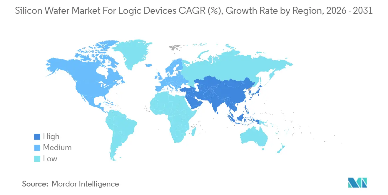
| Fastest Growing Market | Asia Pacific |
| Largest Market | Asia Pacific |
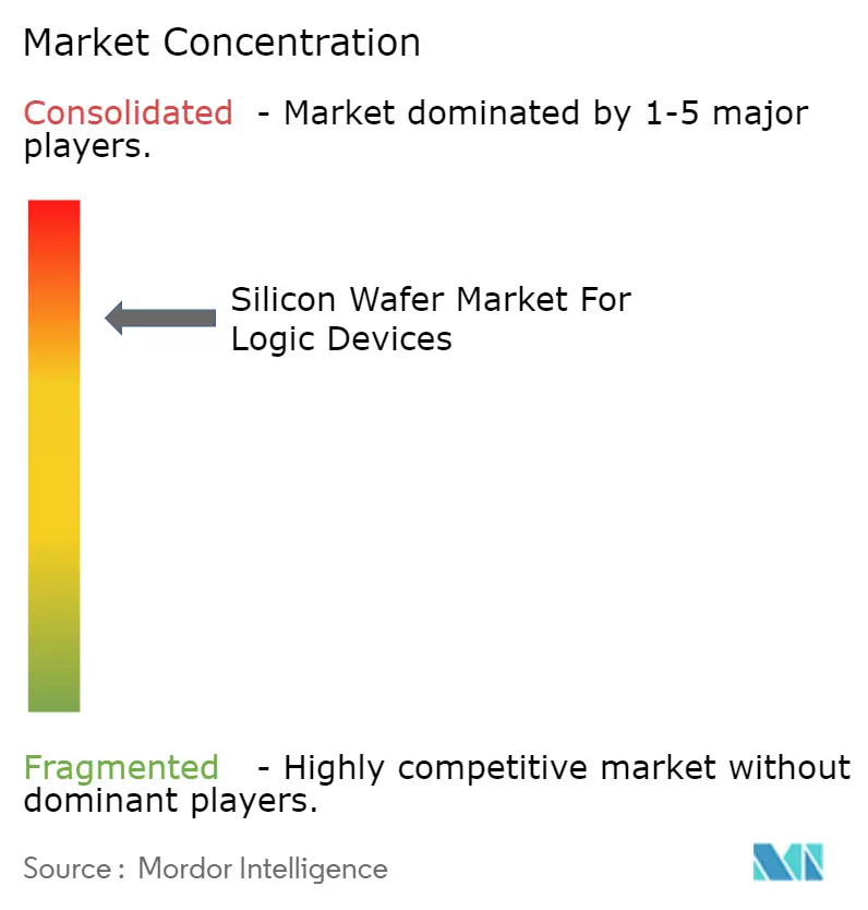
| Market Concentration | High |
Major Players *Disclaimer: Major Players sorted in no particular order Image © Mordor Intelligence. Reuse requires attribution under CC BY 4.0. | |
Silicon Wafer for Logic Devices Market Analysis by Mordor Intelligence
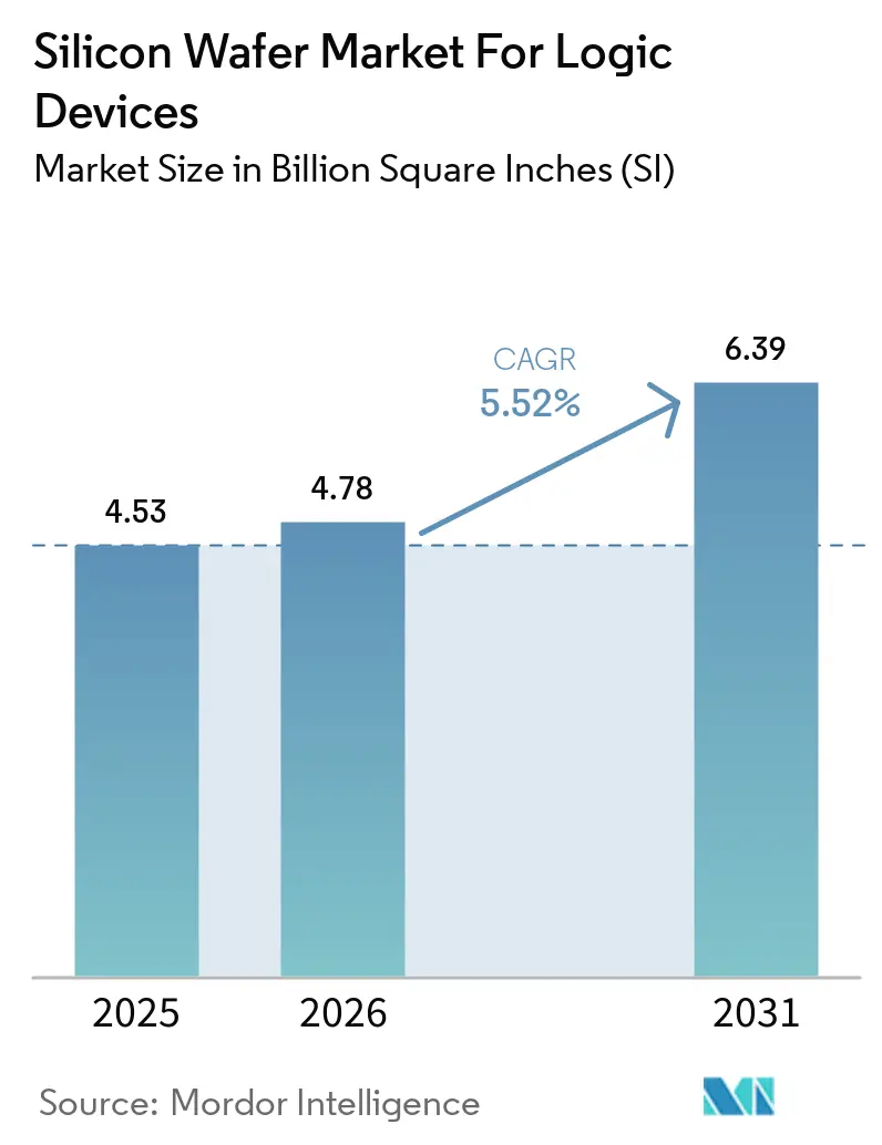
The Silicon Wafer for Logic Devices Market market size is projected to be 4.53 billion square inches in 2025, 4.78 billion square inches in 2026, and reach 6.39 billion square inches by 2031, growing at a CAGR of 5.52% from 2026 to 2031. Rapid migration toward advanced-node manufacturing, the dominance of 300 mm substrates, and sizable government incentives in the United States, the European Union, and South Korea underpin this expansion. Investments in extreme ultraviolet lithography, backside power delivery, and gate-all-around transistor structures are redefining substrate flatness and purity benchmarks, while wafer suppliers co-locate near new front-end fabs to compress qualification cycles. Asia-Pacific maintains volume leadership, but North America and Europe are building indigenous capacity to reduce single-region dependence. Capital barriers remain steep, yet opportunities are opening in specialty substrates such as silicon-on-insulator and ultra-thin wafers for advanced packaging. In this environment, the Silicon Wafer for Logic Devices Market market is poised for steady growth as logic demand broadens from smartphones to artificial-intelligence servers and connected vehicles.
Key Report Takeaways
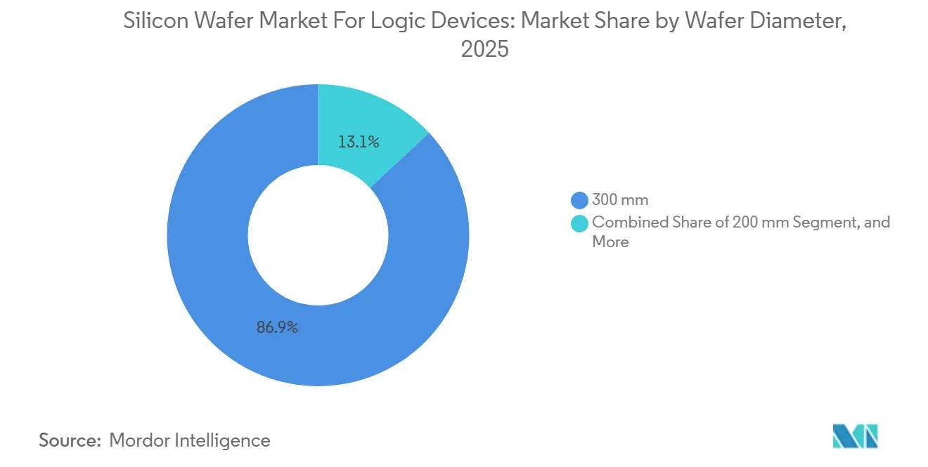
- By wafer diameter, 300 mm captured 86.87% of the Silicon Wafer for Logic Devices Market market share in 2025, while 300 mm wafer shipments are forecast to expand at a 6.04% CAGR through 2031.
- By wafer type, prime polished substrates led with 82.73% revenue share in 2025; silicon-on-insulator wafers are the fastest-growing segment, advancing at a 6.42% CAGR to 2031.
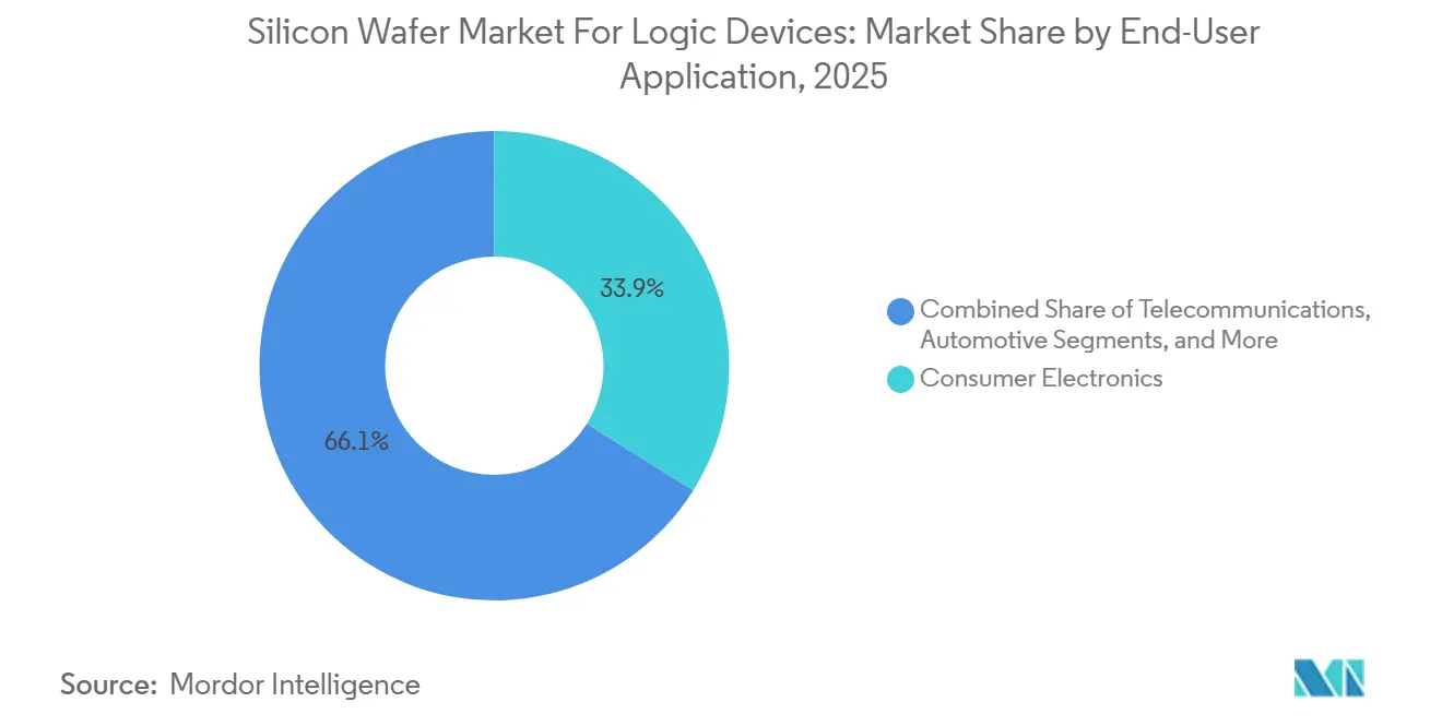
- By end-user, consumer electronics held 33.92% of the 2025 Silicon Wafer for Logic Devices Market market size, whereas telecommunications infrastructure is projected to grow at a 6.51% CAGR over 2026-2031.
- By geography, Asia-Pacific held 78.68% of the Silicon Wafer for Logic Devices Market market share in 2025. Asia-Pacific is projected to advance at a 6.17% CAGR to 2031.
Note: Market size and forecast figures in this report are generated using Mordor Intelligence’s proprietary estimation framework, updated with the latest available data and insights as of January 2026.
Global Silicon Wafer for Logic Devices Market Trends and Insights
Drivers Impact Analysis*
| Driver | (~) % Impact on CAGR Forecast | Geographic Relevance | Impact Timeline |
|---|---|---|---|
| Growing Demand for AI and High-Performance Computing Chips | +1.8% | Global, concentration in North America and Asia-Pacific | Medium term (2-4 years) |
| Transition Toward 3 nm and Below Nodes Using 300 mm Wafers | +1.5% | Asia-Pacific core, spill-over to North America and Europe | Long term (≥ 4 years) |
| Rising Investment in Front-End Fabs Under Government Incentives | +1.2% | North America and Europe, secondary effects in Asia-Pacific | Medium term (2-4 years) |
| Expansion of 5G and IoT Device Production Volumes | +0.9% | Global, early gains in Asia-Pacific and Europe | Short term (≤ 2 years) |
| Backside Power Delivery Architectures Requiring Ultra-Flat Wafers | +0.7% | Asia-Pacific and North America advanced-node fabs | Long term (≥ 4 years) |
| Silicon Photonics Co-Integration in Logic Devices | +0.4% | North America and Europe data-center hubs | Long term (≥ 4 years) |
| Source: Mordor Intelligence | |||
Growing Demand for AI and High-Performance Computing Chips
Hyperscalers are shipping custom accelerators in ever-larger training clusters, and each cluster can consume more than 10,000 substrates per quarter as GPU, networking, and chiplet base dies all originate on 300 mm silicon. Chiplet partitioning increases overall wafer starts because interposer and base dies join the demand profile, even as transistor density rises per chip. Leading-edge foundry nodes such as N3, N2, and 18A report double-digit revenue shares, signaling sustained appetite for ultra-flat, low-defect substrates that ensure high yields.[1]T.-C. Wei, “N3 and N3E Revenue Contribution, 4Q 2025 Earnings,” TSMC, tsmc.com Edge-inference deployments widen the diameter mix by drawing mature 7 nm and 5 nm lines into automotive and industrial environments, pushing total substrate volume higher. This driver therefore reinforces both advanced and mature-node demand streams for the Silicon Wafer for Logic Devices Market market.
Transition Toward 3 nm and Below Nodes Using 300 mm Wafers
The cost of extreme ultraviolet EUV lithography tools in excess of USD 200 million per unit necessitates 300 mm wafer platforms, concentrating capacity and capital on one diameter.[2]H. Niroomand, “EUV System Cost Structure,” ASML, asml.com Gate-all-around nanosheet transistors and backside power delivery networks require epitaxial source-drain regions on substrates with total thickness variation below 0.15 micrometers, tightening flatness requirements well beyond the SEMI M1 baseline. Samsung, Intel, and foundry peers now specify sub-angstrom surface roughness, spurring wafer-maker investment in chemical-mechanical polishing and laser metrology. As nodes shrink, each exposure step tolerates fewer particles, so 300 mm crystal defect density must trend downward, locking in a higher value per wafer and sustaining the Silicon Wafer for Logic Devices Market market.
Rising Investment in Front-End Fabs Under Government Incentives
The CHIPS and Science Act and the European Union Chips Act have collectively allocated well over USD 100 billion in grants and tax credits, compressing typical fab construction schedules to under three years and catalyzing parallel investments in local substrate output.[3]U.S. Department of Commerce, “2025 CHIPS Act Awards,” commerce.gov Wafer suppliers are colocating near these projects to simplify logistics and accelerate equipment qualification, fragmenting a supply chain once centered in Japan and Taiwan. This geographic diversification enhances resilience yet leads to overlapping build-outs, increasing aggregate demand for pullers, epitaxy, and polishing tools, which amplifies growth for the Silicon Wafer for Logic Devices Market market.
Expansion of 5G and IoT Device Production Volumes
Fifth-generation networks reached 5.9 billion subscriptions in 2025 and are tracking toward 7.5 billion by 2028, raising silicon content per handset and multiplying the number of base-station chipsets per square kilometer.[4]Ericsson Mobility Report, ericsson.com IoT nodes surpass 30 billion devices by 2027, shifting mature-node volume toward 300 mm as 200 mm tool sets age. Automotive IoT contributes additional wafer starts through connected-vehicle microcontrollers and sensor hubs fabricated on mixed-signal processes. Collectively, these deployments broaden the application base, further supporting revenue visibility in the Silicon Wafer for Logic Devices Market market.
Restraints Impact Analysis*
| Restraint | (~) % Impact on CAGR Forecast | Geographic Relevance | Impact Timeline |
|---|---|---|---|
| High Capital Expenditure for 300 mm Wafer Capacity | -0.9% | Global, acute pressure in North America and Europe | Medium term (2-4 years) |
| Supply Chain Disruptions in Polysilicon and Specialty Gases | -0.7% | Global, concentration risk in Asia-Pacific | Short term (≤ 2 years) |
| Limited Availability of Ultra-High-Purity Float-Zone Silicon | -0.3% | Global, niche RF and sensor segments | Long term (≥ 4 years) |
| Stricter Water-Use Regulations in Major Fab Locations | -0.2% | North America and Taiwan | Medium term (2-4 years) |
| Source: Mordor Intelligence | |||
High Capital Expenditure for 300 mm Wafer Capacity
A greenfield 300 mm wafer plant requires USD 3 billion-USD 5 billion upfront, and equipment depreciation spans 10-15 years, increasing financial risk for prospective entrants.[5]J. Fuchs, “Global Capex Requirements for 300 mm Substrates,” Siltronic, siltronic.com Rising interest rates in 2024-2025 lifted weighted-average cost of capital by up to 200 basis points, delaying expansion at second-tier suppliers. GlobalWafers’ USD 5 billion Texas fab, announced in 2025 yet slated for 2028 ramp, underlines the long payback cycles that constrain supply elasticity.[6]GlobalWafers, “Texas Fab Project Overview,” globalwafers.com High capex narrows the field to five dominant vendors, moderating competitive pricing in the Silicon Wafer for Logic Devices Market market.
Supply Chain Disruptions in Polysilicon and Specialty Gases
China supplied roughly 85% of global polysilicon in 2025, and spot prices moved from USD 8 to USD 12 per kilogram within one quarter, unsettling wafer cost structures. Japan opened antidumping probes into Chinese dichlorosilane in January 2026, risking tariffs on a key epitaxial gas.[7]Ministry of Economy, Trade and Industry Japan, “Announcement of Dichlorosilane Investigation,” meti.go.jp Environmental crackdowns idled chlorosilane capacity in 2025, while the Russia-Ukraine conflict squeezed neon and krypton availability for lithography lasers. Wafer firms now lock multiyear gas contracts and install on-site purification, solutions that add 5%-8% to operating expenses, tempering margins in the Silicon Wafer for Logic Devices Market market.
*Our forecasts treat driver/restraint impacts as directional, not additive. The impact forecasts reflect baseline growth, mix effects, and variable interactions.
Segment Analysis
By Wafer Diameter: Economies of Scale Cement 300 mm Dominance
The 300 mm class held 86.87% of 2025 shipments and is advancing at a 6.04% CAGR, underscoring its structural cost advantage in the Silicon Wafer for Logic Devices Market market. A single 300 mm wafer yields nearly 2.4 times the die count of a 200 mm substrate of equal design, lowering cost per transistor by up to 40%. All leading-edge capacity additions through 2031 are earmarked for this diameter, channeling supplier capex and reinforcing a virtuous cycle of scale.
Foundries still operate 200 mm lines for power-management, analog, and MEMS circuits, but equipment obsolescence and tool scarcity are pushing even these workloads onto 300 mm. Sub-150 mm wafers now account for less than 5% of logic shipments, making them a legacy niche. As Siltronic and SK Siltron shutter 150 mm production by 2027, slow-moving aerospace and military programs will bear re-qualification costs, yet mainstream economics leave suppliers few alternatives, solidifying 300 mm leadership within the Silicon Wafer for Logic Devices Market market.


By Wafer Type: SOI Gains Share in Low-Power Logic
Prime polished substrates delivered 82.73% of 2025 shipments, but silicon-on-insulator volume is climbing fastest at a 6.42% CAGR, pulled by mobile processors and RF front-ends. The buried oxide layer in SOI reduces parasitic capacitance and cuts standby power by roughly 25%, a crucial edge in battery-constrained devices. CEA-Leti’s December 2025 thin-film bonding breakthrough promises further leakage cuts, positioning SOI for deeper penetration.
Epitaxial wafers serve high-voltage and image-sensor markets, keeping a stable 12% share, while high-resistivity float-zone slices fill RF switch and sensor niches. Capacity bottlenecks in float-zone furnaces lengthen lead times beyond 12 months, discouraging entry. Segment growth thus hinges on specialty capacity build-outs, but the underlying mix still favors prime polished, preserving majority share in the Silicon Wafer for Logic Devices Market market.
By End-User Application: Telecommunications Outpaces Consumer Electronics
Consumer electronics commanded 33.92% of 2025 volume, driven by flagship smartphones migrating to 3 nm application processors. Yet telecommunications infrastructure is rising faster at a 6.51% CAGR as 5G densification and Open RAN multiply logic content per cell site. Massive-MIMO antennas integrate beamforming ASICs on advanced nodes, raising area per base station by a factor of three relative to 4G.
Automotive logic demand is accelerating as domain controllers move from 28 nm to 5 nm, evident in TSMC’s USD 6.8 billion automotive revenue for 2024. Industrial and IoT sensors prefer mature nodes but remain tethered to the 300 mm migration of foundry fleets. Outside these verticals, medical and defense maintain long-horizon supply deals, absorbing older diameter wafers yet presenting limited volume uplift for the Silicon Wafer for Logic Devices Market market.
Geography Analysis
Asia-Pacific retained 78.68% shipment share in 2025 and is expanding at 6.17% CAGR through 2031 as Taiwan, South Korea, and mainland China extend advanced-node capacity. TSMC alone consumed more than 1 million 300 mm wafers monthly across 13 fabs, and two additional Kaohsiung plants come online by 2028. Samsung’s Hwaseong campus entered 2 nm production in late 2025, while SK Siltron increased Gumi pulls to serve domestic customers. China’s drive for self-reliance maintains demand despite export controls, aided by local suppliers Ferrotec and Shanghai Simgui.
North America is re-emerging, powered by USD 52.7 billion in CHIPS Act grants. Intel’s Arizona and Ohio projects plus TSMC’s Phoenix complex will together draw roughly 400,000 wafers per month by 2027. GlobalWafers’ Texas plant, slated for 2028, marks the first large-scale domestic substrate output in two decades, shrinking logistics lead times. Sustainability rules tighten water-use metrics; TSMC Arizona already recycles 65% of process water, a benchmark regulators look to codify.
Europe accounted for under 10% of 2025 shipments but is accelerating as the EUR 43 billion (USD 48.6 billion) EU Chips Act sponsors Intel’s Magdeburg dual-fab, TSMC’s Dresden joint venture with Bosch, and STMicroelectronics, GlobalFoundries FD-SOI expansion in Crolles. Long-term take-or-pay wafer contracts underpin these ventures, lifting regional demand and adding diversity to the Silicon Wafer for Logic Devices Market market. South America and the Middle East and Africa remain peripheral, though sovereign funds in Saudi Arabia considered partnership in 2025 to seed a regional hub, a move watched closely by substrate vendors evaluating long-range diversification.

Competitive Landscape
Five vendors, Shin-Etsu Chemical, SUMCO, GlobalWafers, Siltronic, and SK Siltron, control roughly 90% of 300 mm capacity, delivering high concentration in the Silicon Wafer for Logic Devices Market market. Competitive differentiation hinges on Czochralski crystal quality, epitaxial layer uniformity, and polishing precision. Shin-Etsu’s magnetic Czochralski process suppresses oxygen precipitation, commanding 5%-10% price premiums for high-performance computing substrates. SUMCO leverages automotive-grade qualification to mitigate commodity swings, with 2025 shipments to vehicle-electronics customers up 25%.
Government incentives open pathways for geographic entrants: GlobalWafers’ USD 5 billion Texas project and Siltronic’s EUR 2 billion Singapore expansion add redundant capacity outside Japan and Taiwan. Specialty niches present growth off-ramps; Soitec’s SOI patent moat spans over 3,000 filings, yet CEA-Leti’s 2025 room-temperature bonding demonstration could halve SOI costs, threatening incumbent economics.
Technological arms races in metrology sharpen quality focus. AI-enhanced optical inspection now flags sub-10 nm particles in real time, cutting scrap rates by nearly 20% and enabling tighter flatness specs for backside power architectures. SEMI’s M1 update, expected in 2026, will formalize backside flatness rules, likely favoring suppliers already validating sub-0.05 µm nanotopography, thereby preserving high entry thresholds within the Silicon Wafer for Logic Devices Market market.
Silicon Wafer for Logic Devices Industry Leaders
Shin-Etsu Handotai Co., Ltd.
SUMCO Corporation
GlobalWafers Co., Ltd.
Siltronic AG
SK Siltron Co., Ltd.
- *Disclaimer: Major Players sorted in no particular order

Recent Industry Developments
- March 2026: Japan’s Ministry of Economy, Trade and Industry launched antidumping probes into Chinese dichlorosilane imports, a move that may alter specialty gas flows across Asia-Pacific.
- December 2025: CEA-Leti demonstrated room-temperature SOI wafer bonding, claiming 40%-50% cost reduction potential and sub-0.5-volt device operation readiness.
- November 2025: TSMC unveiled plans for two new 300 mm fabs in Kaohsiung, with 2 nm and 1.4 nm output scheduled for 2028.
- October 2025: GlobalWafers secured USD 400 million in CHIPS Act grants for its USD 5 billion Texas wafer plant, targeting 2028 production.


Global Silicon Wafer for Logic Devices Market Report Scope
The Silicon Wafer for Logic Devices Market Report is Segmented by Wafer Diameter (≤150mm, 200mm, and 300mm), Wafer Type (Prime Polished, Epitaxial, Silicon-on-Insulator, and Specialty Silicon (High-Resistivity, Power, Sensor-Grade)), End-user Application (Consumer Electronics, Industrial, Telecommunications, Automotive, Other End-user Applications), and Geography (North America, Europe, Asia-Pacific, South America, Middle East and Africa). The Market Forecasts are Provided in Terms of Shipment Area (Billion Square Inches).
| ≤150 mm |
| 200 mm |
| 300 mm |
| Prime Polished |
| Epitaxial |
| Silicon-on-Insulator (SOI) |
| Specialty Silicon (High-Resistivity, Power, Sensor-Grade) |
| Consumer Electronics | Mobile and Smartphones |
| PCs and Servers | |
| Industrial | |
| Telecommunications | |
| Automotive | |
| Other End-user Applications |
| North America | United States |
| Canada | |
| Mexico | |
| Europe | Germany |
| United Kingdom | |
| France | |
| Rest of Europe | |
| Asia-Pacific | China |
| Japan | |
| India | |
| South Korea | |
| Taiwan | |
| Rest of Asia-Pacific | |
| South America | |
| Middle East and Africa |
| By Wafer Diameter | ≤150 mm | |
| 200 mm | ||
| 300 mm | ||
| By Wafer Type | Prime Polished | |
| Epitaxial | ||
| Silicon-on-Insulator (SOI) | ||
| Specialty Silicon (High-Resistivity, Power, Sensor-Grade) | ||
| By End-user Application | Consumer Electronics | Mobile and Smartphones |
| PCs and Servers | ||
| Industrial | ||
| Telecommunications | ||
| Automotive | ||
| Other End-user Applications | ||
| By Geography | North America | United States |
| Canada | ||
| Mexico | ||
| Europe | Germany | |
| United Kingdom | ||
| France | ||
| Rest of Europe | ||
| Asia-Pacific | China | |
| Japan | ||
| India | ||
| South Korea | ||
| Taiwan | ||
| Rest of Asia-Pacific | ||
| South America | ||
| Middle East and Africa | ||


Key Questions Answered in the Report
What is the projected size of the Silicon Wafer for Logic Devices Market in 2031?
The Silicon Wafer for Logic Devices Market market size is forecast to reach 6.39 billion square inches by 2031.
Which wafer diameter will dominate production through 2031?
The 300 mm format will remain dominant, retaining more than 85% shipment share and growing at a 6.04% CAGR.
Why are silicon-on-insulator wafers gaining momentum?
SOI substrates cut standby power by roughly 25%, meeting mobile and RF power budgets and therefore post the fastest 6.42% CAGR.
How do government incentives influence wafer supply chains?
Programs like the CHIPS and Science Act and the EU Chips Act accelerate local fab construction and prompt wafer makers to co-locate, expanding regional diversity.
What factors restrict new entrants into large-diameter wafer production?
USD 3 billion-USD 5 billion capex per plant, 10-15-year depreciation cycles, and stringent purity specifications keep barriers high.
Which end-user segment shows the fastest growth through 2031?
Telecommunications infrastructure leads end-user growth with a projected 6.51% CAGR as 5G densification raises silicon content per base station.
Page last updated on:


