Extreme Ultraviolet Lithography Market Size and Share
Market Overview
| Study Period | 2020 - 2031 |
|---|---|
| Market Size (2026) | USD 25.93 Billion |
| Market Size (2031) | USD 40.54 Billion |
| Growth Rate (2026 - 2031) | 9.35% CAGR |
| Fastest Growing Market | Middle East and Africa |
| Largest Market | Asia Pacific |
| Market Concentration | High |
Major Players
*Disclaimer: Major Players sorted in no particular order Image © Mordor Intelligence. Reuse requires attribution under CC BY 4.0. |
|

Extreme Ultraviolet Lithography Market Analysis by Mordor Intelligence
The extreme ultraviolet lithography market size in 2026 is estimated at USD 25.93 billion, growing from the 2025 value of USD 23.71 billion, with 2031 projections showing USD 40.54 billion, growing at a 9.35% CAGR over 2026-2031. Growth comes from chipmakers’ shift to nodes below 5 nm, where EUV reduces process steps and line-edge roughness. Rising demand from AI, 5G, and high-performance computing keeps fab utilization high and accelerates equipment orders. Public funding under the CHIPS and European Chips Acts improves access to capital and encourages geographically diverse fabs. Suppliers are moving to High-NA exposure tools that print sub-8 nm features, even though those scanners cost about USD 384 million each. At the same time, component breakthroughs such as carbon-nanotube pellicles and energy-efficient light sources promise higher throughput and lower operating cost, reinforcing the strategic role of the EUV lithography market in advanced semiconductor manufacturing.
Key Report Takeaways
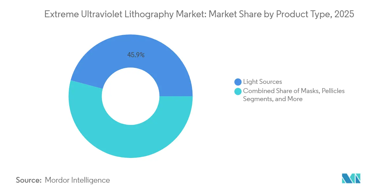
- By product type, Light Sources led with 45.85% of the EUV lithography market share in 2025; pellicles are projected to expand at an 17.9% CAGR through 2031.
- By end-user type, foundries held 52.75% of the EUV lithography market share in 2025, while IDMs are forecast to advance at a 13.6% CAGR to 2031.
- By technology node, the 5 nm class accounted for 33.75% of the EUV lithography market size in 2025; the 2 nm and below node is expected to rise at a 20.2% CAGR between 2026-2031.
- By light-source technology, LPP controlled 87.95% of the EUV lithography market size in 2025; ERL-EUV sources are set to grow at a 26.1% CAGR through 2031.
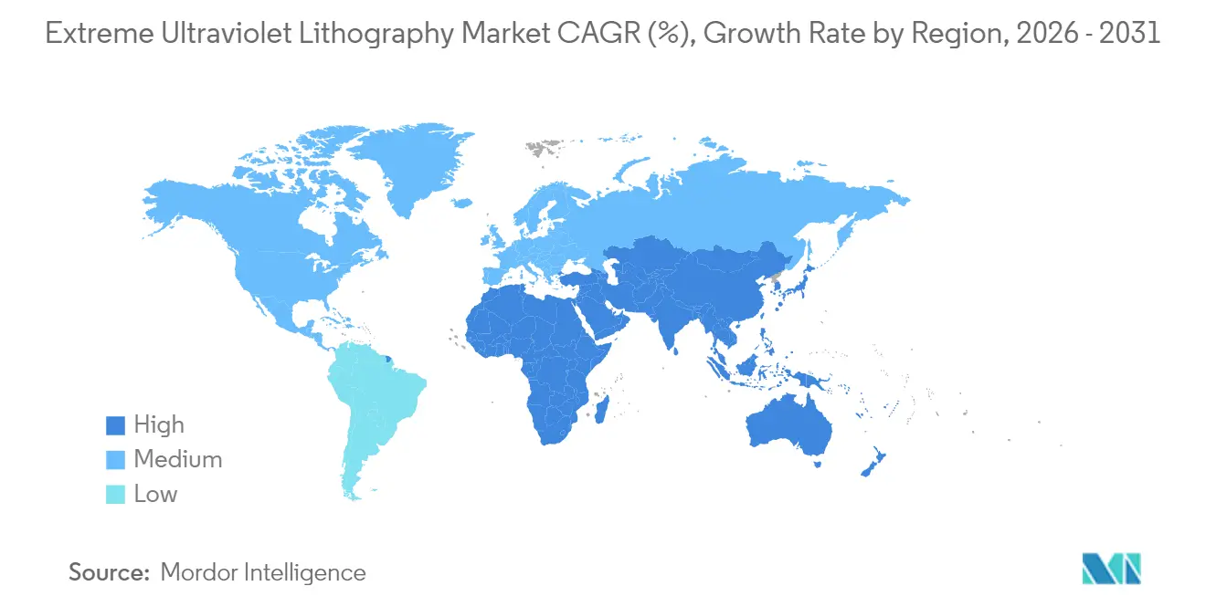
- By geography, Asia-Pacific captured 63.85% revenue share in 2025; the Middle East and Africa region is projected to post an 10.9% CAGR to 2031.
Note: Market size and forecast figures in this report are generated using Mordor Intelligence’s proprietary estimation framework, updated with the latest available data and insights as of 2026.
Global Extreme Ultraviolet Lithography Market Trends and Insights
Drivers Impact Analysis*
| Driver | (~) % Impact on CAGR Forecast | Geographic Relevance | Impact Timeline |
|---|---|---|---|
| Demand for < 5 nm logic and memory nodes | +3.8% | Global, with a concentration in Asia-Pacific | Medium term (2-4 years) |
| Accelerated AI/5G/HPC capacity build-out | +2.4% | North America, Asia-Pacific | Short term (≤ 2 years) |
| Government semiconductor subsidy programs | +1.7% | North America, Europe, Asia-Pacific | Medium term (2-4 years) |
| Transition to High-NA (0.55 NA) EUV platforms | +1.2% | Global | Long term (≥ 4 years) |
| Productivity leap from pellicle membrane breakthroughs | +0.8% | Global | Medium term (2-4 years) |
| ERL-based compact EUV light-source R&D momentum | +0.5% | North America, Asia-Pacific | Long term (≥ 4 years) |
| Source: Mordor Intelligence | |||


Demand for Sub-5 nm Nodes
Mass-production plans for 2 nm chips scheduled for 2025 call for line widths that only EUV exposure can achieve. TSMC has set aside USD 12.3 billion for its EUV tool fleet, a budget that targets 10-15% speed gains or 25-30% power cuts versus 3 nm designs.[1]Techovedas, “TSMC Invests Over USD 12.3 Billion in EUV,” techovedas.com Smartphone and data-center chip buyers have already queued for those nodes, allowing equipment vendors to lock in multi-year backlogs. As a result, the EUV lithography market enjoys a predictable shipment pipeline that mirrors each successive node shrink.
Accelerated AI/5G/HPC Capacity Build-out
AI accelerators, 5G base-band silicon, and high-bandwidth memory all need tight pitch metallization. TSMC’s Q4 2024 revenue rose 37% year-on-year to USD 26.88 billion, illustrating the scale of demand. To keep pace, the company budgeted USD 32-36 billion for capex in 2025, including roughly 60 EUV scanners. Such orders shorten tool lead times and bring smaller suppliers—pellicle, mask blank, and resist vendors—into the growth loop of the EUV lithography market.
Government Semiconductor Subsidy Programs
The U.S. CHIPS Act is funneling USD 52 billion into domestic production, with USD 825 million set aside for an EUV Accelerator in New York. Europe seeks to double its semiconductor share to 20% by 2030, and Japan pairs its subsidy regime with alliances on GAAFET research. These policies tilt capital flows toward new greenfield fabs, broadening the geographical customer base for EUV exposure tools and ancillary components.
Transition to High-NA EUV Platforms
ASML shipped the first 0.55 NA scanner to Intel in late 2023. The platform raises density by 2.9× versus 0.33 NA tools, trimming the number of patterning steps per wafer. Early adopters locked in all units through mid-2025, guaranteeing a multi-year revenue stream. Although each system costs USD 384 million, projected productivity gains offset the purchase by lowering mask count and improving yield.
Restraints Impact Analysis*
| Restraint | (~) % Impact on CAGR Forecast | Geographic Relevance | Impact Timeline |
|---|---|---|---|
| USD 150 m+ system cost and fab retrofit complexity | -3.2% | Global | Medium term (2-4 years) |
| Single-vendor dependency and supply-chain bottlenecks | -2.1% | Global | Short term (≤ 2 years) |
| Stochastic defectivity of EUV photoresists | -1.1% | Global | Medium term (2-4 years) |
| Scarcity of EUV-trained field service engineers | -0.9% | Global, with a concentration in Asia-Pacific | Short term (≤ 2 years) |
| Source: Mordor Intelligence | |||
USD 150 m+ System Cost and Fab Retrofit Complexity
Baseline EUV scanners list at roughly USD 150 million, and high-NA units more than double that figure. Fabs also upgrade clean-room airflow, vibration damping, and power distribution. Smaller foundries struggle to amortize such outlays, risking a technology gap that narrows potential customers for the EUV lithography market. Dual-lane operations, where DUV and EUV run in parallel, further enlarge capital budgets.
Single-Vendor Dependency and Supply-Chain Bottlenecks
ASML owns 100% of the EUV system supply and 90% of the DUV base. Output is capped near 50 tools per year, and export controls restrict shipments to some regions. Critical subsystems—from high-purity glass to multi-layer mirrors—face similar single-source exposure. Any disruption reverberates across the EUV lithography market, prompting governments to invest in domestic component capacity to mitigate risk.
*Our forecasts treat driver/restraint impacts as directional, not additive. The impact forecasts reflect baseline growth, mix effects, and variable interactions.
Segment Analysis
By Product Type: Light Sources Drive Revenue, Pellicles Accelerate Growth
Light sources accounted for 45.85% of the EUV lithography market size in 2025, underscoring their status as the most expensive subsystem in a scanner. Current laser-produced-plasma (LPP) modules convert CO₂-laser pulses and tin droplets into 13.5 nm radiation, but sub-5% conversion efficiency continues to spur research into free-electron alternatives. High average power also drives upgrades such as advanced collector-mirror coatings and debris filters, with service contracts that guarantee power stability, adding annuity revenue for suppliers.
Pellicles are the fastest-growing product, with an 17.9% CAGR projected through 2031. Carbon-nanotube membranes now deliver 97-98% transmittance and withstand 1,000 W exposure, a step change from earlier silicon-nitride films. Major foundries have cleared CNT pellicles for 2 nm process flows, opening a replacement cycle in which every mask layer needs protection; rising scale is already trimming unit cost.


By End-User Type: IDMs Challenge Foundry Dominance
Foundries accounted for 52.75% of the EUV lithography market in 2025 because fab-less customers rely on contract manufacturing. Their specialization lets them order scanners in batches, lock in service capacity, and co-develop processes with tool suppliers. TSMC alone controlled 56% of installed EUV exposure capacity, translating geographic clustering in Taiwan into supply-chain efficiencies and learning-curve cost reductions.
IDMs, however, are expanding faster at a 13.6% CAGR. Intel’s IDM 2.0 model reopens its fabs to external clients while adding High-NA capacity reserved through 2025. Subsidy grants lower its effective capital cost, narrowing the unit-cost gap with pure-play foundries. As IDMs upgrade to gate-all-around transistors, they internalize design-process feedback loops, an advantage that should lift their share of the EUV lithography market over the decade.
By Technology Node: 2 nm and Below Drives Future Growth
The 5 nm node held 33.75% of the EUV lithography market share in 2025, benefiting from mature yields and broad platform support across mobile and datacenter chips. Cost per transistor remains favorable versus 3 nm when productivity bonuses and mask savings are included. Still, roadmaps now center on 2 nm platforms that promise 25-30% energy savings. The segment is forecast to expand at a 20.2% CAGR to 2031, the highest in the hierarchy, as leading customers preload demand for AI and edge-compute processors.
Gate-all-around architectures at 2 nm require tighter overlay control and lower stochastics, both served by EUV’s one-pass imaging. Early pilot lines report line-edge roughness within spec at full-field exposure. Research consortia are fine-tuning high-NA optics and new resists to hold pattern fidelity despite reduced process windows, cementing EUV lithography market relevance for every successive node shrink.

By Light-Source Technology: ERL-EUV Disrupts LPP Dominance
LPP units comprised 87.95% of total shipments in 2025, standardizing the infrastructure of CO₂ lasers, droplet generators, and collector mirrors. Incremental upgrades have nudged average power toward 500 W, enough for most 3 nm mass production. Vendors bundle debris filters to improve mirror life and reduce unscheduled maintenance, bolstering tool utilization across the EUV lithography market.
ERL-EUV platforms, projected to clock a 26.1% CAGR, eliminate tin debris by generating coherent EUV in a superconducting linac. Lawrence Livermore research indicates 2 kW output at 0.33 GeV beam energies, slashing wall-plug power draw. Prototype timelines align with the industry’s 1.4 nm node, giving chipmakers an alternative that could diversify supply. If commercialized, ERL technology would lower operating costs and environmental footprint, two priorities for subsidy-backed green fabs.
Geography Analysis
Asia-Pacific led the EUV lithography market with 63.85% of 2025 revenue. Taiwan’s TSMC alone has installed roughly 60 scanners financed by the USD 12.3 billion EUV budget noted above. Samsung’s Korean fabs will bring their first High-NA tool online in Q1 2025. Japanese suppliers such as Hoya remain the primary source of EUV mask blanks, further reinforcing regional clustering.
North America is gaining momentum. The CHIPS Act earmarks USD 825 million for an EUV Accelerator in Albany, while Intel’s High-NA roll-out benefits from early access to all first-wave scanners. Department of Energy grants fund next-generation light-source research at Lawrence Livermore National Laboratory, positioning the region as an innovation hub.
The Middle East and Africa region, although starting from a small base, is forecast to grow at an 10.9% CAGR to 2031 as sovereign wealth funds in the UAE and Saudi Arabia invest in AI infrastructure that will ultimately require advanced chip supply. Early memoranda with U.S. tool vendors cover pilot fabs and clean-room engineering, leaving open a path to EUV adoption once ecosystems mature.

Regulatory Landscape
Export controls and national-security rules shape EUV lithography supply and deployment most directly. In the United States, the Department of Commerce Bureau of Industry and Security (BIS) issued a major semiconductor package in December 2024 that expanded Entity List designations and added new controls spanning multiple categories of semiconductor manufacturing equipment and related software. The change increased licensing and screening requirements for cross-border shipments tied to advanced-node production.
Allied policy alignment further tightens availability of advanced lithography tools and selected adjacent systems. The Netherlands expanded and updated its national export control measure for advanced semiconductor manufacturing equipment in September 2024 and continued tightening in 2025 through authorization requirements covering a broader range of advanced tools. In May 2026, BIS also issued guidance clarifying the scope of license requirements for advanced computing items for entities tied to Country Group D:5 or Macau, adding additional due-diligence expectations for firms operating across multinational corporate structures.
Value Chain Analysis
The EUV lithography value chain is concentrated around a small set of critical, single-source subsystems. ASML is the sole provider of EUV scanners, with Carl Zeiss SMT supplying the projection optics and Cymer (an ASML subsidiary) supplying EUV light-source modules. These modules integrate high-power drive lasers supplied primarily by Trumpf to generate 13.5 nm radiation from tin droplet plasma.
Upstream specialty materials and components such as masks, mask blanks, pellicles, photoresists, and ultra-stable optics inputs remain essential gating items, while downstream demand is anchored by leading foundries and IDMs that qualify tools, masks, and process materials for 7 nm through 2 nm and below production flows. Bottlenecks increasingly sit in capacity, qualification, and lead-time management rather than broad availability of substitute suppliers. Japan is a central hub for EUV photoresists, with Tokyo Ohka Kogyo, JSR, and Shin-Etsu Chemical collectively holding a dominant share. The transition toward High-NA also increases dependence on tightly matched mask inspection and metrology workflows. In response to AI-driven tool demand, ASML has publicly targeted reductions in EUV system build cycle time (from about 22 weeks to about 15-16 weeks) and outlined EUV capacity expansion steps into 2027 and 2028, reinforcing how manufacturing throughput and constrained specialist supplier capacity influence delivery schedules and installed-base growth.
Competitive Landscape
Market concentration is extreme, as ASML is the sole supplier of EUV scanners after investing USD 9 billion in cumulative R&D. Scanner prices rose 22% between 2020 and 2022, reflecting strong demand and limited capacity. Closed co-development loops tie ASML to Zeiss SMT for optics and to Cymer for light sources, while multiyear purchase agreements allocate supply among TSMC, Samsung, and Intel.
Component makers target adjacent niches: Zeiss adds adaptive mirror stages, chemical suppliers refine metal-oxide resists, and Imec hosts pilot-line testing under a five-year pact with ASML.[4]Imec, “Imec and ZEISS Sign New Strategic Partnership Agreement,” imec-int.com U.S. CHIPS Act funding expands Corning’s ultra-low-expansion glass output, easing a mirror-blank bottleneck.
Geopolitics also reshapes demand. Export controls restrict latest-generation scanners from select Chinese fabs, prompting domestic alternatives and parallel DUV investments. European and U.S. policymakers answer with regional tool ecosystems, and the five-year ASML–Imec partnership formalizes knowledge sharing while pursuing sustainability goals. Over the medium term, EUV supply is likely to remain single-sourced, yet emerging light-source and pellicle vendors could fragment adjacent segments.
Extreme Ultraviolet Lithography Industry Leaders
-
ASML Holding NV
-
ZEISS SMT
-
Gigaphoton Inc.
-
Cymer LLC
-
Canon Inc.
- *Disclaimer: Major Players sorted in no particular order


Market Opportunities and Future Outlook
A near-term opportunity is scaling High-NA EUV from early deployments into production-layer insertion and supporting infrastructure. That expansion broadens demand beyond scanners into masks, pellicles, optics, and mask qualification tools that require tighter matching for sub-2 nm patterning. In July 2026, ASML disclosed a readiness milestone tied to the first high-volume logic product using its High-NA EUV platform in collaboration with Intel Foundry, which indicates adjacent spending on High-NA compatible mask and process ecosystems is advancing alongside the tool roadmap rather than staying confined to pilot lines.
Another opportunity is productivity and supply-chain de-risking work that translates into incremental demand for critical subsystems and materials within the report scope. ASML has stated plans to raise EUV production capacity by 30% in 2027 and evaluate a further step-up for 2028, along with actions to shorten build cycle time. Those steps increase the addressable pull for light-source components, mirrors/optics, and mask-related consumables required for tool delivery and ramp. At the same time, research signals for below-2 nm patterning create whitespace for advanced resists and mask solutions; for example, IBM researchers presented High-NA EUV process capability work at SPIE 2026, supporting qualification cycles for new materials and process windows that can reduce stochastic defectivity and improve yield at tighter nodes.
Recent Industry Developments
- July 2026: ASML announced a High-NA EUV readiness milestone tied to the first high-volume logic product manufactured with its EXE platform in collaboration with Intel Foundry. The update marked a transition from early tool installs toward production-relevant insertion, reinforcing demand for High-NA capable masks, pellicles, and optics that can support tighter process windows.
- September 2025: ZEISS SMT introduced AIMS EUV 3.0 to the market for EUV photomask qualification, positioning the platform to raise throughput and support both Low-NA and High-NA EUV environments. Wider availability of mask qualification capacity supports faster mask learning cycles and closer scanner matching as EUV layers increase at advanced nodes.
- September 2024: Canon shipped its FPA-1200NZ2C nanoimprint lithography (NIL) system to the Texas Institute for Electronics (TIE) for research and prototyping. The delivery strengthened a US-based consortium testbed for alternative patterning approaches, which can complement EUV in selected use cases while keeping advanced lithography R&D activity high.


Research Methodology Framework and Report Scope
Market Definition and Coverage
For this methodology, the market covers revenue linked to extreme ultraviolet (EUV) lithography used in semiconductor manufacturing, including core tool-enabling components that make EUV patterning possible at advanced nodes.
Scope exclusions: Older lithography technologies, general wafer fab tools outside EUV patterning, and downstream semiconductor packaging equipment are not counted here.
Segmentation Overview
-
By Product Type
- Light Sources
- Mirrors / Optics
- Masks
- Pellicles
- Mask Blanks
-
By End-User Type
- Foundries
- Integrated Device Manufacturers (IDMs)
-
By Technology Node
- 7 nm and above
- 5 nm
- 3 nm
- 2 nm and below
-
By Light-Source Technology
- Laser-Produced Plasma (LPP)
- Gas-Discharge Plasma
- Vacuum Spark
- ERL-EUV
-
By Geography
-
North America
- United States
- Canada
-
South America
- Brazil
- Rest of South America
-
Europe
- Germany
- Netherlands
- United Kingdom
- France
- Italy
- Russia
- Rest of Europe
-
Asia-Pacific
- Taiwan
- South Korea
- Japan
- China
- Singapore
- Rest of Asia-Pacific
-
Middle East and Africa
-
Middle East
- GCC
- Turkey
- Saudi Arabia
- Rest of Middle East
-
Africa
- South Africa
- Rest of Africa
-
Middle East
-
North America
Data Sources, Market Sizing, and Validation
Desk Research
Desk work was used to set the outer boundaries for demand, supply timing, and pricing logic before any model math was finalized. We leaned on public manufacturing and trade signals that tend to move with advanced-node spending, and then checked them against industry facts that are consistently reported year to year.
Examples of sources reviewed include SEMI publications, World Semiconductor Trade Statistics (WSTS) releases, International Trade Administration (US Department of Commerce) updates, U.S. International Trade Commission data, and OECD industrial indicators. In addition, we reviewed company annual reports, earnings call transcripts, investor presentations, and reputable electronics manufacturing press for shipment timing, capacity additions, and lead-time commentary. Patent databases were also referenced to understand the pace of key EUV subsystem development and when it appears to be moving from lab to commercial adoption. The desk sources listed here are illustrative only, and many other public and paid references were used for collection, cross-checking, and clarification.
Primary Interviews and Surveys
Primary conversations were used to pressure-test the model where public data is thin, especially around tool shipment pacing, subsystem attach rates, and how pricing shifts as nodes move from early ramp to broader production. We spoke with a mix of equipment-side and buyer-side experts, covering foundries and IDMs. The interviews were spread across APAC, EMEA, and the Americas, so regional investment cycles were not overfit to one geography.
Distribution of primary research fieldwork respondents
| Company type | Respondent position | Region |
|---|---|---|
| Top tier: 39% | CXOs: 14% | APAC: 45% |
| Mid tier: 43% | Functional/Unit leaders: 40% | EMEA: 37% |
| Smaller Players: 18% | Managers: 46% | Americas: 18% |
Market-Sizing & Forecasting
The core build starts from a top-down demand reconstruction that tracks advanced-node capacity build-outs and the EUV intensity of those ramps, which is then converted into tool-and-component revenue using typical tool throughput, shipment cadence, and replacement and service timing. To keep the outputs realistic, results are then corroborated with selective bottom-up approximations, such as sampled ASP times estimated unit shipments and cross-checks against a small set of supplier revenue disclosures.
Inputs used in the model include leading-edge fab capacity additions, the pace of node transitions (for example, 7 nm and below), expected EUV tool shipment schedules, subsystem content assumptions across light sources, mirrors, and masks, and pricing trends tied to productivity and yield learning. Where the bottom-up view is incomplete (for example, when subsystem revenue is not separately disclosed), gaps are handled through attach-rate ranges validated in expert calls and then constrained by the total spend envelope implied by fab investment plans.
For forecasting, scenario analysis is used, with a base case that reflects the most common expert view on timing of new fab ramps and tool deliveries, and then we run conservative and aggressive cases around shipment delays, export control effects, and ASP movement. The final forecast is kept traceable so each year moves mainly because the underlying capacity and tool demand signals move.
Data Validation & Update Cycle
Outputs are validated through multiple checks so the totals do not rely on one assumption. We compare modeled revenue against independent signals such as advanced-node capacity announcements, capital spending trends, and reported commentary on EUV tool lead times, and then investigate any large variance before sign-off.
A second analyst review is completed to re-check formulas, currency handling, and year-on-year movement logic, followed by a final consistency pass across regions and end users. The report is refreshed annually, and interim updates are made when there are material events like major shipment delays, policy changes, or step-changes in fab expansion plans. Before delivery, a last-mile refresh is performed so clients receive the latest updated view available at that time.
Mordor Intelligence's Extreme Ultraviolet Lithography Market Sizing Compared With Other Published Estimates
Published market values for EUV lithography can look far apart because the scope line is drawn differently, and because timing assumptions (shipment recognition vs installed base effects) are not handled the same way. Currency year, what is counted as EUV revenue, and how quickly pricing is assumed to move can also shift the final number by a lot.
The table points to a spread that is mostly explained by what is counted inside EUV and when it is recognized as revenue. Under Mordor Intelligence's scope, the 2024 value includes revenue across key EUV product types like light sources, mirrors, and masks, which tends to lift totals versus figures that only count scanners or that strip out major subsystems. It can also sit above estimates that apply faster ASP declines during early adoption years.
Benchmark comparison
| Source | Market Size | Gaps in Research Methodology |
|---|---|---|
| Mordor Intelligence | USD 10.34 B (2024) | |
| Industry Research Portal A | USD 2.94 B (2024) | Uses a narrower revenue boundary that appears closer to tool-only counting, and it mixes unit shipment views with revenue sizing, which can understate subsystem-heavy spend in years with strong component attach. |
| Press Release Digest B | USD 7.27 B (2024) | Applies a different inclusion mix across product types and may treat pricing and shipment timing more aggressively, which can compress the current-year value even if the long-term growth rate is higher. |
Across the three values, the biggest driver is scope, followed by how shipment timing and ASP movement are treated in the early ramp period. By keeping the build tied to visible fab ramp signals and then cross-checking with supplier-side revenue cues, our estimate stays explainable and repeatable even when disclosure detail varies.


Key Questions Answered in the Report
What is the current size and growth outlook of the EUV lithography market?
The market is valued at USD 25.93 billion in 2026 and is projected to reach USD 40.54 billion by 2031, reflecting a 9.35% CAGR.
Which product segment is expected to grow the fastest through 2031?
Pellicles, driven by carbon-nanotube membranes, show the highest momentum with an 17.9% CAGR forecast for 2026-2031.
How do High-NA scanners affect capital budgets?
Each 0.55 NA tool costs about USD 384 million, more than double standard EUV units, but boosts transistor density 2.9×, reducing multi-patterning and long-run wafer cost.
Which geography leads demand, and which region is expanding quickest?
Asia-Pacific controls 63.85% of 2025 revenue, while the Middle East and Africa region is set to rise at an 10.9% CAGR to 2031 as new tech investments gain traction.
What are the primary barriers to wider EUV adoption?
High system price and fab retrofit complexity (-3.2% impact on forecast CAGR) and single-vendor dependency (-2.1% impact) are the most significant hurdles.
Page last updated on: