Plasma Etching Equipment Market Size and Share
Market Overview
| Study Period | 2020 - 2031 |
|---|---|
| Market Size (2026) | USD 14.34 Billion |
| Market Size (2031) | USD 20.42 Billion |
| Growth Rate (2026 - 2031) | 7.32% CAGR |
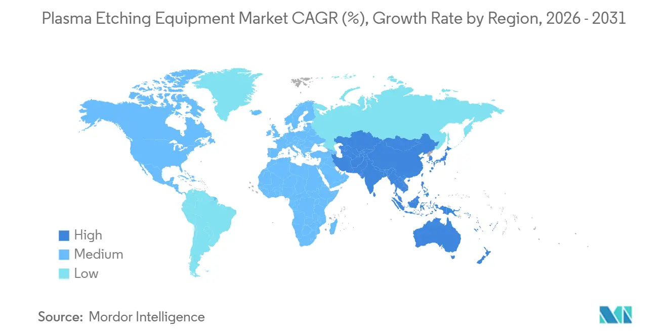
| Fastest Growing Market | Asia Pacific |
| Largest Market | Asia Pacific |
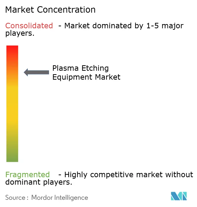
| Market Concentration | High |
Major Players *Disclaimer: Major Players sorted in no particular order Image © Mordor Intelligence. Reuse requires attribution under CC BY 4.0. | |
Plasma Etching Equipment Market Analysis by Mordor Intelligence
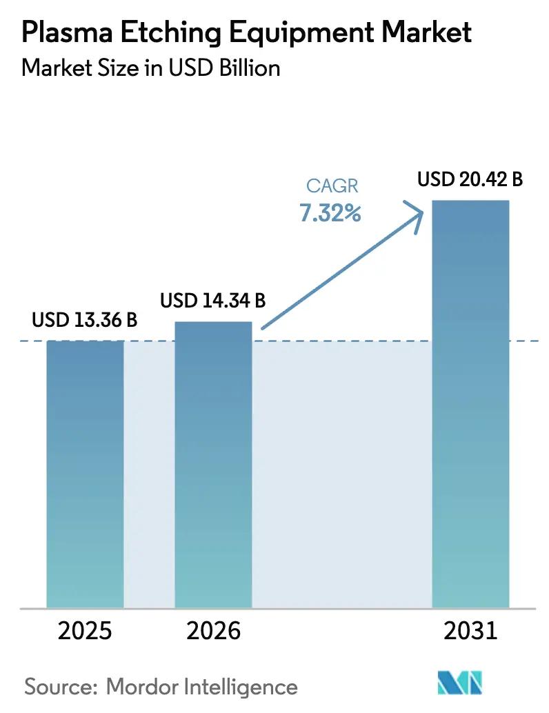
The Plasma Etching Equipment Market size is projected to be USD 13.36 billion in 2025, USD 14.34 billion in 2026, and reach USD 20.42 billion by 2031, growing at a CAGR of 7.32% from 2026 to 2031.
Demand is scaling as extreme ultraviolet lithography migrates into 3 nm production and 3-dimensional memory architectures surpass 200 vertical layers, both of which require aspect-ratio control beyond 100:1. Inductively coupled plasma tools dominate because their low-pressure, high-density plasmas protect fragile gate dielectrics while sustaining vertical sidewalls. Deep reactive ion platforms are gaining momentum, particularly through-silicon via formation for advanced packaging, and atomic layer approaches are transitioning from pilot lines to volume production. Government incentives in the United States, European Union, Japan, and South Korea are accelerating tool orders, while silicon carbide and gallium nitride adoption in electric vehicles and 5G infrastructure is diversifying material needs.
Key Report Takeaways
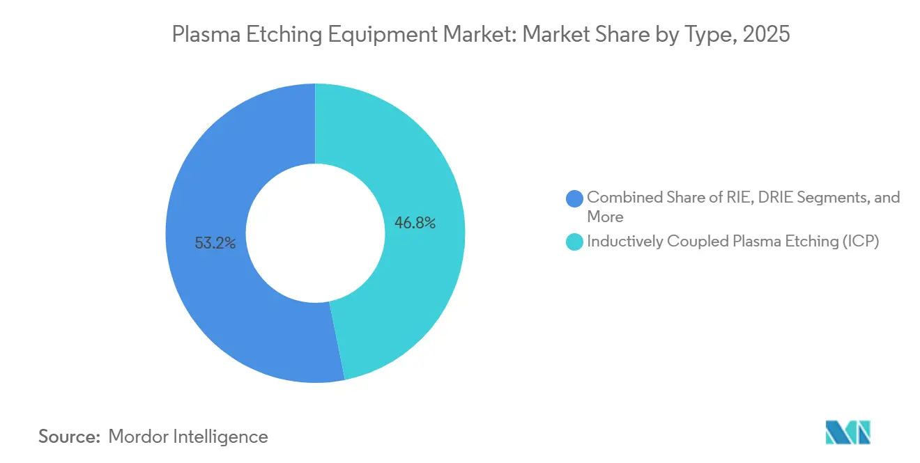
- By type, inductively coupled plasma systems commanded 46.83% of 2025 revenue, while deep reactive ion technology is on track to post a 7.99% CAGR through 2031.
- By wafer size, the 300 mm format secured 51.73% revenue share in 2025 and above-450 mm is projected to expand at 8.33% as cost-per-die considerations intensify.
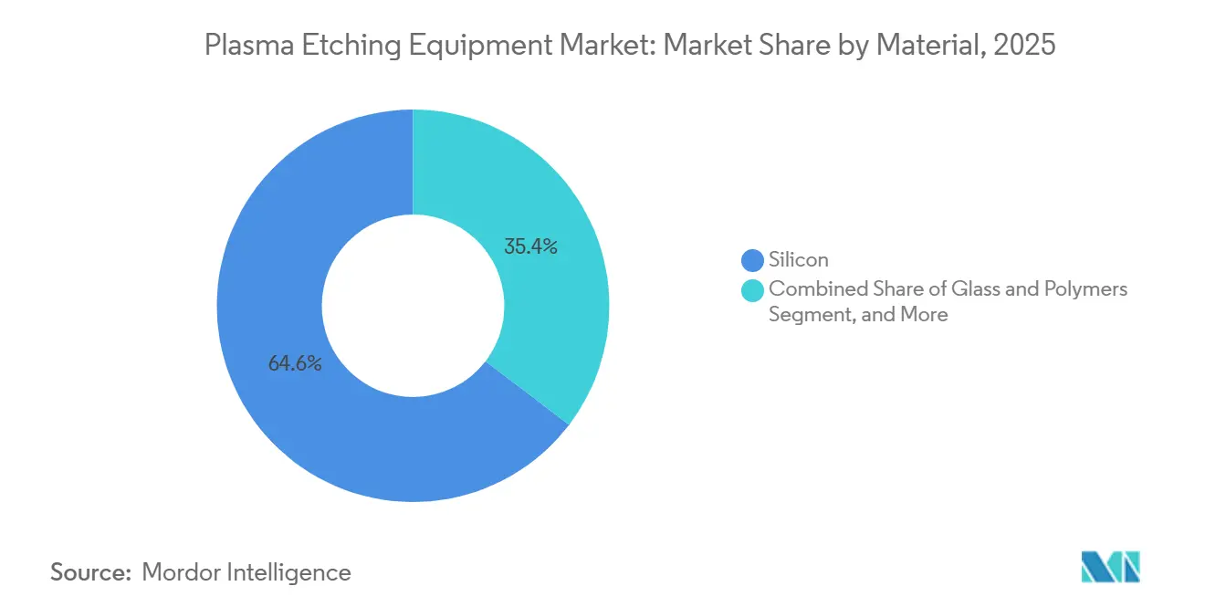
- By material, silicon captured 64.63% demand in 2025 whereas compound substrates are forecast to grow 8.56% annually on rising silicon carbide and gallium nitride use.
- By application, consumer electronics led with 38.61% revenue share in 2025; automotive electronics is expected to log a 7.88% CAGR to 2031 on electrification tailwinds.
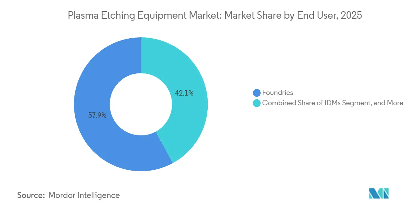
- By end user, foundries held 57.94% of 2025 spending and are set to deliver an 8.51% CAGR through 2031 as fabless design houses increase outsourcing.
- By geography, Asia-Pacific generated 55.72% of 2025 revenue and is on course for an 8.66% CAGR through 2031 owing to capacity additions in Taiwan, South Korea, Japan, and China.
Note: Market size and forecast figures in this report are generated using Mordor Intelligence’s proprietary estimation framework, updated with the latest available data and insights as of January 2026.
Global Plasma Etching Equipment Market Trends and Insights
Drivers Impact Analysis*
| Driver | (~) % Impact on CAGR Forecast | Geographic Relevance | Impact Timeline |
|---|---|---|---|
| Expansion of EUV Lithography Driving High Aspect-Ratio Etch Requirements | +1.8% | Asia-Pacific core, North America and Europe leading-edge fabs | Medium term (2-4 years) |
| Proliferation of 3D NAND and DRAM Node Shrinks | +1.6% | Asia-Pacific (South Korea, Japan, China), selective North America | Medium term (2-4 years) |
| Growing Demand for Compound-Semiconductor Power Devices | +1.4% | Global, with concentration in Europe and Asia-Pacific automotive hubs | Long term (≥ 4 years) |
| Government-Backed Chip Sovereignty Programs (US CHIPS Act, EU Chips Act) | +1.3% | North America and Europe, spillover to allied nations | Short term (≤ 2 years) |
| Shift Toward Heterogeneous Integration and Advanced Packaging | +1.0% | Global, led by Asia-Pacific foundries and North America design houses | Medium term (2-4 years) |
| Emerging Use in Quantum Computing Device Fabrication | +0.3% | North America and Europe research clusters | Long term (≥ 4 years) |
| Source: Mordor Intelligence | |||
Expansion of EUV Lithography Driving High Aspect-Ratio Etch Requirements
Extreme ultraviolet lithography transitioned from pilot lines to high-volume manufacturing at the 3 nm node in 2025 and is slated for adoption at the 2 nm node by 2027. Each EUV step increases etch intensity because contact holes, vias, and gate spacers now require aspect ratios exceeding 120:1, with critical dimensions below 10 nm.[1]ASML, “Q1 2025 Results,” asml.com ASML shipped 20 EUV scanners in Q1 2025, a 33% year-over-year increase, and every scanner is paired with multiple inductively coupled plasma chambers. IBM validated nanosheet transistors that require 14 separate etch steps per gate stack, doubling complexity over finFET nodes.[2]IBM Research, “2 nm Chip Technology,” ibm.com Capital outlays for etch tools consequently rose to 18-22% of total fab spending in 2025. Tool makers are embedding real-time endpoint spectroscopy to suppress micro-trenching, and fabs are revising recipe libraries to execute ultra-low bias processes that cut sidewall bowing to within 1 degree.
Proliferation of 3D NAND and DRAM Node Shrinks
Samsung disclosed a 286-layer vertical NAND product in 2024 that necessitates etch depths exceeding 15 µm with sub-2-degree taper, magnifying demand for deep reactive ion equipment calibrated to mitigate aspect-ratio-dependent lag.[3]Samsung Electronics, “286-Layer V-NAND Announcement,” samsung.com SK Hynix adopted atomic layer etching to protect high-k dielectrics in its 1-alpha-nm DRAM, launched in 2025. Meanwhile, cryogenic processes cooled below 0 °C are being qualified to improve selectivity between silicon oxide and nitride. SEMI estimated memory companies spent USD 45 billion on capital equipment in 2025, 20% of which was devoted to etch platforms.[4]SEMI, “World Fab Forecast 2025,” semi.org High layer counts in 3D NAND and shrinking capacitor pitches in DRAM will keep etch process steps rising each year through 2031.
Growing Demand for Compound-Semiconductor Power Devices
Silicon carbide and gallium nitride power devices migrated to 200 mm and 300 mm wafers in 2025, driving a new wave of equipment capable of handling chemically inert substrates at temperatures exceeding 400 °C. Infineon ramped a 300 mm silicon carbide line in Malaysia with goals to halve cost per ampere by 2027. Onsemi announced a 300 mm silicon carbide fab in the Czech Republic to enter volume production in late 2026, further broadening the customer base for high-temperature plasma chambers. Electric vehicles are forecast to incorporate USD 1,200 of semiconductor content per unit by 2030, with power devices accounting for approximately 30% of that value, thereby elevating compound substrates as a growth engine.
Government-Backed Chip Sovereignty Programs
The United States CHIPS and Science Act, the EU Chips Act, and analogous incentives in Japan and South Korea collectively exceed USD 100 billion and are compressing fab construction timelines. Intel’s Ohio site broke ground in September 2024 following USD 8.5 billion in U.S. grants, and etch tool move-in is scheduled for the second half of 2026. Taiwan Semiconductor Manufacturing Company’s Arizona project secured USD 6.6 billion in direct funding and advanced its second fab start date to 2027. The European Union allocated EUR 43 billion (USD 46.7 billion) with the aim of doubling regional chip output by 2030. These incentives guarantee near-term tool orders and require domestic service hubs, prompting Applied Materials and Lam Research to expand spare-parts depots in Arizona and Saxony.
Restraints Impact Analysis*
| Restraint | (~) % Impact on CAGR Forecast | Geographic Relevance | Impact Timeline |
|---|---|---|---|
| Plasma-Induced Damage in Sub-5 nm Structures | -1.2% | Global, concentrated in leading-edge fabs (Asia-Pacific, North America) | Short term (≤ 2 years) |
| Rising Clean-Room Construction and Utility Costs | -0.9% | North America and Europe, moderate impact in Asia-Pacific | Medium term (2-4 years) |
| Supply Chain Volatility for High-Purity Specialty Gases | -0.7% | Global, acute in regions with limited domestic gas production | Short term (≤ 2 years) |
| IP Restrictions Limiting Equipment Exports to China | -0.6% | China primary impact, secondary effects on global equipment utilization | Medium term (2-4 years) |
| Source: Mordor Intelligence | |||
Plasma-Induced Damage in Sub-5 nm Structures
Lattice defects, charge accumulation, and interface roughness caused by ion bombardment during etch steps cut drive current and shift threshold voltage when the gate oxide thickness approaches 1 nm. Atomic layer etching reduces damage but triples the cycle time, thereby increasing the cost per wafer. Tokyo Electron’s latest atomic layer platform removes 0.5 nm per cycle but requires approximately 200 cycles to clear a 10 nm trench, compared to 30 seconds for a continuous plasma etch. Fabs are therefore limiting atomic layer methods to the most sensitive layers while accepting controlled damage in less critical regions.
Rising Clean-Room Construction and Utility Costs
Leading-edge fabs in the United States and Europe cost USD 20 billion or more, roughly double Asia-Pacific equivalents, driven by labor scarcity, environmental permitting, and higher energy tariffs. Intel’s Ohio investment estimate rose from USD 20 billion to USD 28 billion by mid-2025 as steel and specialized clean-room material prices climbed. Utility costs, especially electricity, remain 40-60% higher than in Taiwan or South Korea, extending payback periods from five to seven years and pushing some integrated device manufacturers to slow expansion schedules.
*Our forecasts treat driver/restraint impacts as directional, not additive. The impact forecasts reflect baseline growth, mix effects, and variable interactions.
Segment Analysis
By Type: Inductively Coupled Plasma Leads While Deep Reactive Ion Accelerates
Inductively coupled plasma platforms generated the largest plasma etching equipment market size contribution at 46.83% in 2025. Their capacity to decouple ion energy from plasma density lets fabs fine-tune anisotropy and protect fragile fins and nanosheets. Deep reactive ion equipment, projected to grow at a 7.99% CAGR through 2031, is key for through-silicon vias and wafer-level packaging that require depths of 50-100 µm at aspect ratios of greater than 20:1, thereby expanding the plasma etching equipment market share held by this segment. Conventional reactive ion tools remain in demand at mature nodes but are gradually migrating toward trailing-edge foundry lines.
Lam Research’s Sense.i platform employs machine learning for real-time bias adjustments that have raised yield by roughly 3 percentage points in contact-hole etch since 2025. Applied Materials added in-situ metrology to its Centris Sym3 to cut chamber-to-chamber variation below 0.3 nm, a necessity for 2 nm gate-all-around transistors. This convergence of plasma and data science is blurring legacy boundaries between tool categories and intensifying supplier competition.


By Wafer Size: 300 mm Stays Core, Above-450 mm Gains Momentum
The 300 mm format accounted for 51.73% of 2025 demand, anchoring the plasma etching equipment market size because Taiwan Semiconductor Manufacturing Company, Samsung, and Intel collectively ran more than 50 fabs on this diameter. Above-450 mm pilot work is picking up, and the segment is predicted to grow at 8.33% through 2031 as industry consortia revisit economies of scale. Intel restarted limited 450 mm pathfinding in 2024, seeking a 40% die-count boost per wafer to justify a projected USD 15 billion retrofit.
Compound-semiconductor makers are shifting from 150 mm and 200 mm to 300 mm lines to cut cost per die in silicon carbide and gallium nitride devices, further enlarging 300 mm tool requirements. SEMI released updated standards in June 2025 to certify etch uniformity and defect specifications for compound wafers, guiding suppliers in redesigning chamber materials for corrosive chemistries.
By Material: Silicon Dominates While Compound Substrates Surge
Silicon substrates captured 64.63% revenue in 2025, reflecting their decades-long role as the workhorse of logic and memory. Compound materials are forecast to expand 8.56% annually, widening the plasma etching equipment market share attributed to silicon carbide power devices and gallium nitride radio-frequency amplifiers. Silicon carbide’s thermal conductivity triples that of silicon, enabling junction temperatures over 200 °C in traction inverters, while gallium nitride’s electron mobility multiplies by ten, supporting amplifier power densities above 10 W per mm at millimeter-wave frequencies.
Wolfspeed demonstrated within-wafer etch variation below 3% across 200 mm silicon carbide substrates at its North Carolina fab, a threshold required for automotive qualification. Selective chemistries employing chlorine-based gases and pulsed bias waveforms now deliver 50:1 selectivity between gallium nitride and underlying silicon, illustrating tool makers’ progress in extending inductively coupled plasma platforms to tough materials.
By Application: Consumer Electronics Leads, Automotive Accelerates
Consumer electronics accounted for 38.61% of 2025 demand, maintaining their top spot in the plasma etching equipment market despite smartphone saturation. Automotive electronics, projected to advance at a 7.88% CAGR, is boosting the plasma etching equipment market size due to the increasing penetration of electric vehicles and the adoption of advanced driver assistance systems. Each battery electric vehicle contains two to three times more semiconductors than an internal-combustion model, with power devices and image sensors driving incremental content.
Tesla cut inverter cost 20% by vertically integrating silicon carbide devices across its vehicle lineup, prompting General Motors and others to lock in long-term deals with compound wafer suppliers. Industrial automation, medical devices, and aerospace form diverse tail segments, each valuing plasma etch precision but contributing lower aggregate volumes.
By End User: Foundries Continue to Expand, Integrated Device Manufacturers Stabilize
Foundries accounted for 57.94% of 2025 spending and are poised for an 8.51% CAGR to 2031 as fabless design houses such as NVIDIA, AMD, and Qualcomm amplify outsourcing. Taiwan Semiconductor Manufacturing Company allocated roughly USD 5.8 billion to etch tools in its USD 32 billion 2025 capex plan. Samsung installed nearly 120 new chambers in Hwaseong to enable gate-all-around production. Integrated device manufacturers, such as Intel, Micron, and SK Hynix, balance internal and external capacity, while university cleanrooms drive atomic layer etch research into emerging materials.
The outsourcing trend reflects rising fab construction costs that now exceed USD 20 billion per site, allowing only a handful of corporations to finance leading-edge capacity. Foundry share therefore remains on a steady upward trend, reinforcing the central role of their equipment roadmaps in shaping supplier revenue.
Geography Analysis
The Asia-Pacific region generated 55.72% of the revenue in 2025 and is projected to achieve an 8.66% CAGR, ensuring it continues to dominate the plasma etching equipment market. Taiwan’s cluster yielded USD 160 billion output in 2025, 65% of global foundry revenue. South Korea produced 70% of DRAM and 45% of NAND that year, cementing its position as the memory hub. China, constrained by export controls, accelerated the uptake of domestic tools, with Semiconductor Manufacturing International Corporation and Hua Hong Semiconductor qualifying NAURA and Advanced Micro-Fabrication Equipment systems for 14 nm and 28 nm flows. Japan reignited investment by allocating JPY 2 trillion (USD 13.5 billion) for local capacity, attracting Taiwan Semiconductor Manufacturing Company, Micron, and Western Digital.
North America represented roughly 25% of 2025 demand and is projected to grow 7.8% as CHIPS Act funds underwrite fabs in Arizona, Ohio, New York, and Texas. Intel’s two-fab Ohio campus alone is expected to need more than 200 etch chambers by 2028. Taiwan Semiconductor Manufacturing Company’s Arizona complex will host three fabs with combined capacity of 600,000 wafer starts per year by 2030, all equipped with leading-edge plasma tools.
Europe held about 10% share in 2025 but is aiming to capture 20% of global chip output by 2030 under the EUR 43 billion EU Chips Act allocation. Intel’s Magdeburg project, STMicroelectronics-GlobalFoundries’ French joint facility, and Infineon’s Dresden expansion represent more than EUR 80 billion (USD 87 billion) in announced investments. Middle East and Africa remain in the exploratory phase, with Abu Dhabi and Riyadh pursuing design and packaging hubs. South America’s activity is limited to assembly initiatives in Brazil and Argentina, while Australia and New Zealand contribute research but not large-scale fabrication.

Competitive Landscape
Applied Materials, Lam Research, and Tokyo Electron collectively hold most of the leading-edge plasma etching equipment market share, reflecting high concentration. Applied Materials leverages a Centura installed base exceeding 10,000 chambers, allowing customers to port recipes with minimal re-qualification. Lam Research focuses on etch and deposition integration, supplying bundled process flows that simplify the ramp-up of advanced packaging. Tokyo Electron offers coater-developer and etch clusters in a single suite, streamlining procurement for lithography-adjacent steps.
Chinese suppliers Advanced Micro-Fabrication Equipment and NAURA Technology Group reached 15% domestic share in 2025 but lack the plasma uniformity, endpoint detection, and automation depth required for sub-7 nm nodes. Oxford Instruments, Plasma-Therm, and SPTS target niche opportunities such as atomic layer and cryogenic etching. Patent filings in cryogenic processes rose 40% year over year in 2024, and SEMI’s F47 automation standards update in April 2025 enables cloud-based predictive maintenance, lowering barriers for smaller entrants.
Selectivity in gate-all-around transistor flows is an emerging battleground. Oxford Instruments achieved 150:1 silicon-germanium to silicon selectivity with cyclic hydrogen-fluoride exposure, while Tokyo Electron is piloting pulsed plasma chemistries to surpass 100:1. These breakthroughs could erode incumbent dominance if commercialized at scale by 2027.
Plasma Etching Equipment Industry Leaders
Lam Research Corporation
Applied Materials Inc.
Tokyo Electron Ltd
SPTS Technologies (KLA company)
Oxford Instruments PLC
- *Disclaimer: Major Players sorted in no particular order

Recent Industry Developments
- October 2025: Applied Materials unveiled the Sculpta Vx inductively coupled plasma tool for 2 nm and below, integrating optical emission monitoring with machine-learning control. Initial shipments to Taiwanese and South Korean foundries start Q1 2026.
- September 2025: Lam Research signed a USD 1.2 billion multi-year agreement with Samsung to supply Sense.i etch and deposition systems for 2 nm and 1.4 nm nodes.
- July 2025: Tokyo Electron invested USD 300 million to expand its Yamanashi Technology Center, adding 15 chambers focused on atomic layer and cryogenic etch R&D.
- June 2025: NAURA Technology Group secured a USD 450 million order from Semiconductor Manufacturing International Corporation for inductively coupled plasma systems covering 14 nm and 28 nm lines.


Global Plasma Etching Equipment Market Report Scope
The scope of the study focuses on the market analysis of plasma etching equipment products worldwide. Market sizing encompasses the revenue generated through plasma etching equipment products analyzed worldwide and sold by various market players. The study also tracks the key market parameters, underlying growth influencers, and major vendors operating in the industry, which supports the market estimations and growth rates over the forecast period. the study further analyzes the overall impact of COVID-19 on the ecosystem. The report's scope encompasses market sizing and forecast for segmentation by type, application, and geography.
| Reactive Ion Etching (RIE) |
| Inductively Coupled Plasma Etching (ICP) |
| Deep Reactive Ion Etching (DRIE) |
| High Density Plasma Etching (HDPE) |
| Other Types |
| Below 150 mm |
| 200 mm |
| 300 mm |
| Above 450 mm |
| Silicon |
| Compound Semiconductors |
| Glass and Polymers |
| Other Materials |
| Consumer Electronics |
| Industrial |
| Medical Devices |
| Automotive Electronics |
| Aerospace and Defense |
| Other Applications |
| Foundries |
| Integrated Device Manufacturers (IDMs) |
| Research and Academic Institutions |
| Other End Users |
| North America | United States | |
| Canada | ||
| Mexico | ||
| South America | Brazil | |
| Argentina | ||
| Rest of South America | ||
| Europe | United Kingdom | |
| Germany | ||
| France | ||
| Italy | ||
| Spain | ||
| Rest of Europe | ||
| Asia-Pacific | China | |
| Japan | ||
| India | ||
| South Korea | ||
| Australia and New Zealand | ||
| Rest of Asia Pacific | ||
| Middle East and Africa | Middle East | Saudi Arabia |
| United Arab Emirates | ||
| Turkey | ||
| Rest of Middle East | ||
| Africa | South Africa | |
| Nigeria | ||
| Rest of Africa | ||
| By Type | Reactive Ion Etching (RIE) | ||
| Inductively Coupled Plasma Etching (ICP) | |||
| Deep Reactive Ion Etching (DRIE) | |||
| High Density Plasma Etching (HDPE) | |||
| Other Types | |||
| By Wafer Size | Below 150 mm | ||
| 200 mm | |||
| 300 mm | |||
| Above 450 mm | |||
| By Material | Silicon | ||
| Compound Semiconductors | |||
| Glass and Polymers | |||
| Other Materials | |||
| By Application | Consumer Electronics | ||
| Industrial | |||
| Medical Devices | |||
| Automotive Electronics | |||
| Aerospace and Defense | |||
| Other Applications | |||
| By End User | Foundries | ||
| Integrated Device Manufacturers (IDMs) | |||
| Research and Academic Institutions | |||
| Other End Users | |||
| By Geography | North America | United States | |
| Canada | |||
| Mexico | |||
| South America | Brazil | ||
| Argentina | |||
| Rest of South America | |||
| Europe | United Kingdom | ||
| Germany | |||
| France | |||
| Italy | |||
| Spain | |||
| Rest of Europe | |||
| Asia-Pacific | China | ||
| Japan | |||
| India | |||
| South Korea | |||
| Australia and New Zealand | |||
| Rest of Asia Pacific | |||
| Middle East and Africa | Middle East | Saudi Arabia | |
| United Arab Emirates | |||
| Turkey | |||
| Rest of Middle East | |||
| Africa | South Africa | ||
| Nigeria | |||
| Rest of Africa | |||


Key Questions Answered in the Report
What is the current size of the plasma etching equipment market?
The market reached USD 14.34 billion in 2026 and is on track for USD 20.42 billion by 2031, reflecting a 7.33% CAGR.
Which segment accounts for the largest plasma etching equipment market share?
Inductively coupled plasma platforms led with 46.83% revenue in 2025, thanks to versatility across logic, memory, and advanced packaging.
What is driving future demand for plasma etching tools?
EUV lithography at 3 nm and 2 nm nodes, 3D NAND exceeding 200 layers, and silicon carbide adoption in electric vehicles are expanding etch intensity per wafer.
Which region will grow fastest through 2031?
Asia-Pacific is forecast for an 8.66% CAGR as Taiwan, South Korea, Japan, and China invest heavily in new capacity.
Who are the key suppliers of leading-edge etch equipment?
Applied Materials, Lam Research, and Tokyo Electron collectively deliver more than 80% of tools used at sub-7 nm nodes, while NAURA and Advanced Micro-Fabrication Equipment focus on mature-node demand in China.
Page last updated on:


