Wafer Processing And Assembly Equipment Market Size and Share
Market Overview
| Study Period | 2020 - 2031 |
|---|---|
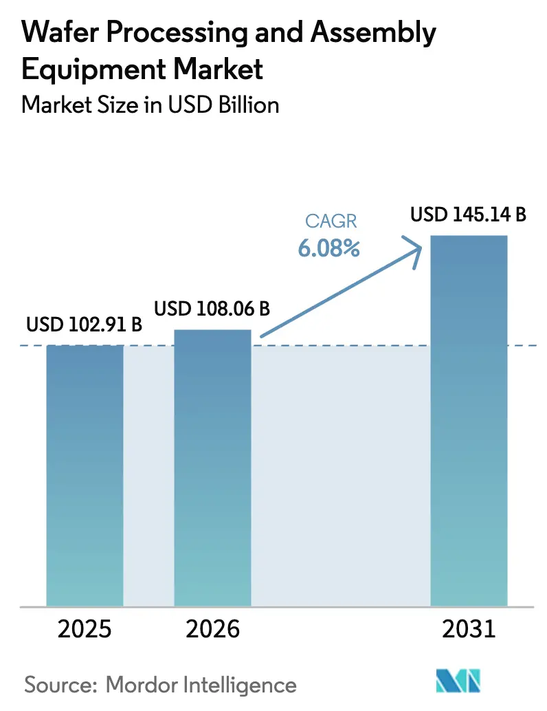
| Market Size (2026) | USD 108.06 Billion |
| Market Size (2031) | USD 145.14 Billion |
| Growth Rate (2026 - 2031) | 6.08% CAGR |
| Fastest Growing Market | Asia-Pacific |
| Largest Market | Asia-Pacific |
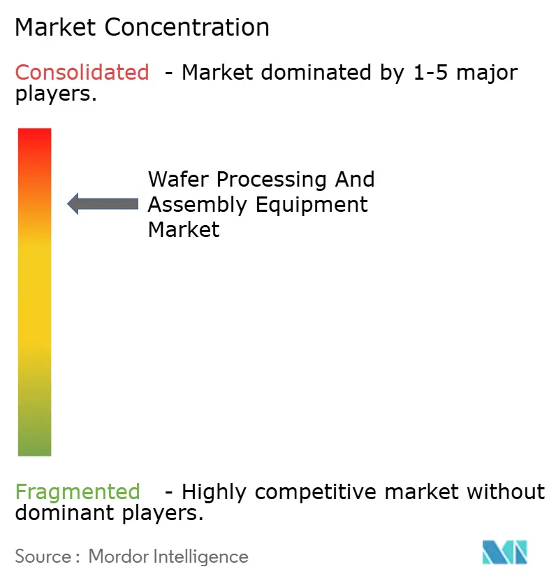
| Market Concentration | High |
Major Players *Disclaimer: Major Players sorted in no particular order Image © Mordor Intelligence. Reuse requires attribution under CC BY 4.0. | |
Wafer Processing And Assembly Equipment Market Analysis by Mordor Intelligence
The Wafer processing and assembly equipment market size was valued at USD 102.91 billion in 2025 and is estimated to grow from USD 108.06 billion in 2026 to reach USD 145.14 billion by 2031, at a CAGR of 6.08% during the forecast period (2026-2031). Ongoing hyperscaler alliances with leading foundries are compressing purchase cycles and anchoring multi-year tool reservations, a pattern that shields vendors from the traditional boom-bust swings of semiconductor investment. High-NA extreme ultraviolet (EUV) lithography is moving from pilot to early production, lifting average selling prices per front-end tool even as fabs seek tighter process-control bundles to curb defect-induced yield loss. Simultaneously, the race toward 300-layer 3D-NAND and 2-nanometer logic nodes is driving incremental steps in deposition, etch, and metrology intensity, while assembly lines pivot toward chiplet-based integration that reshapes back-end capital allocation. Asia-Pacific retains purchasing primacy, yet the CHIPS and Science Act in the United States and the EU Chips Act in Europe are redirecting a growing share of cutting-edge tool shipments toward on-shore green-field fabs.
Key Report Takeaways
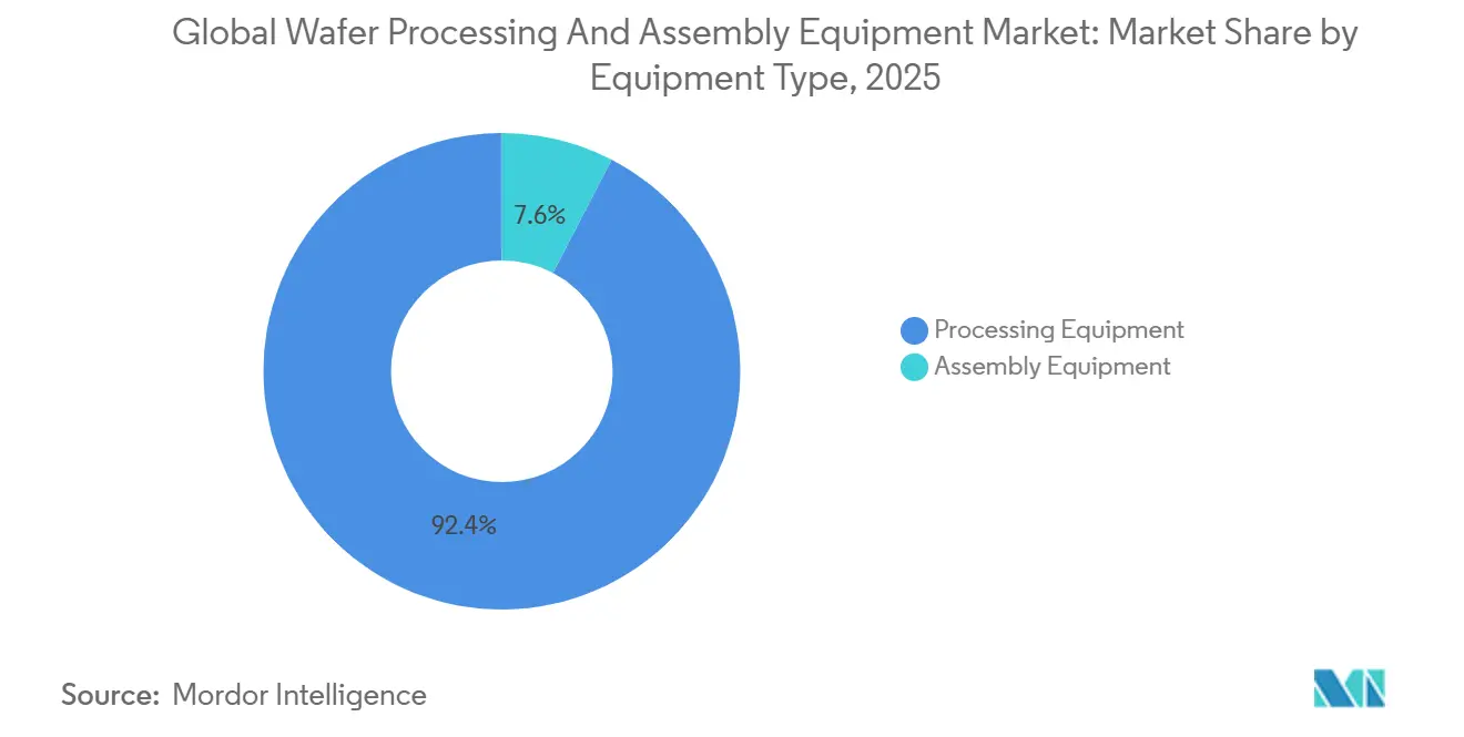
- By equipment type, processing equipment captured 92.39% of 2025 revenue while assembly equipment exhibits the highest growth, expanding at a 6.75% CAGR through 2031.
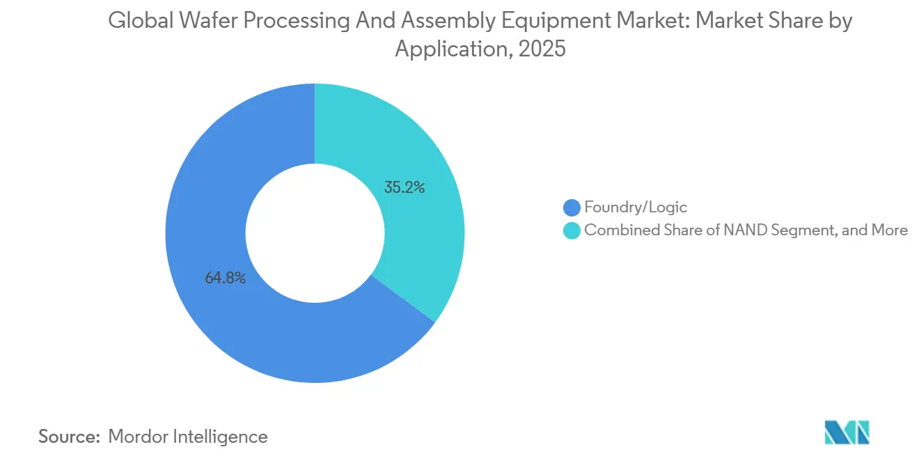
- By application, foundry and logic applications held 64.84% of the 2025 wafer processing and assembly equipment market share, whereas NAND equipment demand is forecast to grow at a 6.98% CAGR to 2031.
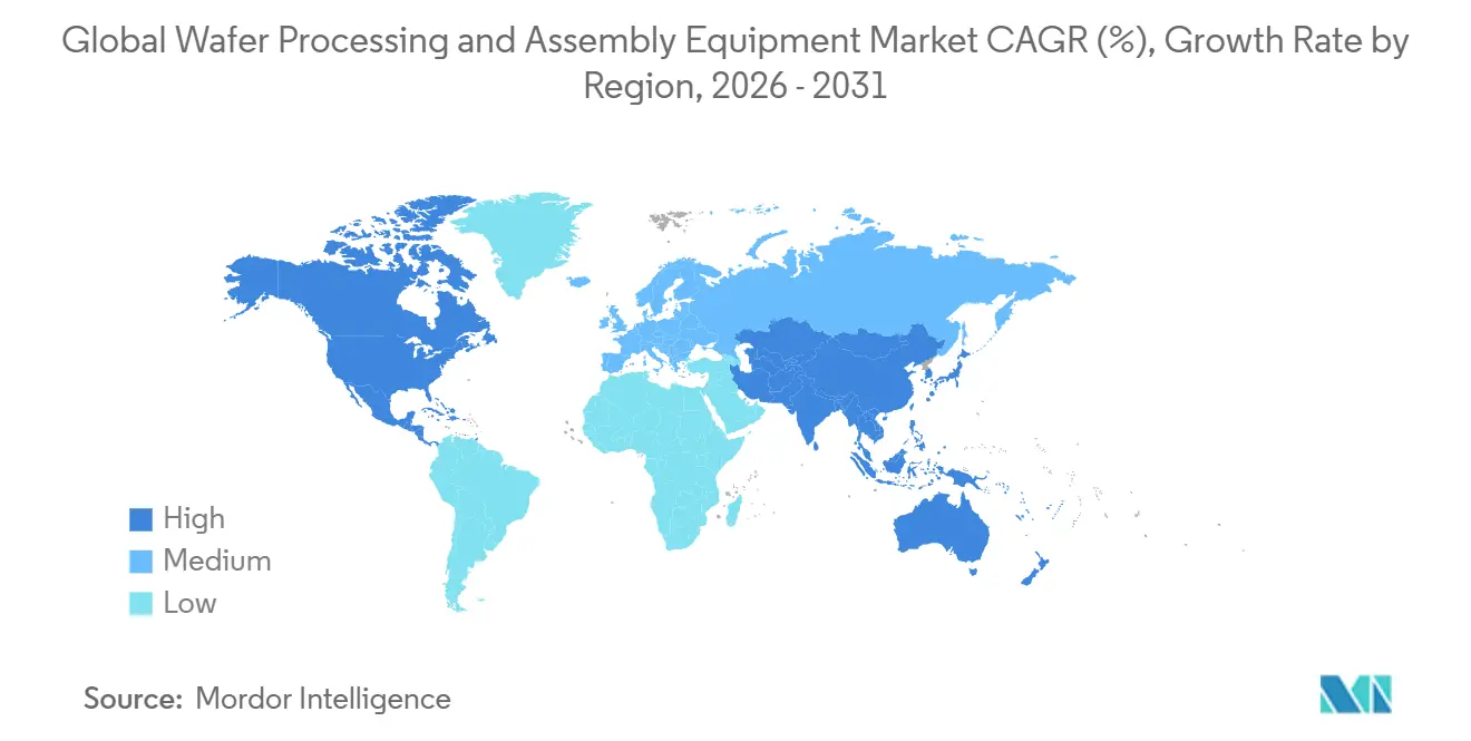
- By geography, Asia-Pacific accounted for 61.28% of 2025 revenue, and North America is projected to post the fastest 6.5% CAGR through 2031.
Note: Market size and forecast figures in this report are generated using Mordor Intelligence’s proprietary estimation framework, updated with the latest available data and insights as of January 2026.
Global Wafer Processing And Assembly Equipment Market Trends and Insights
Drivers Impact Analysis*
| Driver | (~) % Impact on CAGR Forecast | Geographic Relevance | Impact Timeline |
|---|---|---|---|
| Soaring CapEx for AI-Optimized Logic Fabs | +1.8% | Global with focus in Taiwan, United States, South Korea | Medium term (2–4 years) |
| Escalating EUV Lithography Adoption | +1.5% | Taiwan, South Korea, United States, emerging in Japan | Long term (≥ 4 years) |
| Intensifying 3D-NAND Layer Stacking Race | +1.2% | South Korea, Japan, China | Medium term (2–4 years) |
| Government Subsidies for On-Shore Chipmaking | +1.0% | United States, European Union, Japan, India | Long term (≥ 4 years) |
| Hybrid Bonding for 3D-IC Integration | +0.7% | Taiwan, United States, South Korea | Medium term (2–4 years) |
| Panel-Level Packaging Push in Advanced OSATs | +0.5% | Taiwan, China, Southeast Asia | Short term (≤ 2 years) |
| Source: Mordor Intelligence | |||
Soaring CapEx for AI-Optimized Logic Fabs
Hyperscalers are underwriting multi-billion-dollar expansions at leading foundries, locking in EUV, deposition, and metrology slots well before tools leave the factory floor. TSMC raised 2025 capital expenditure to a USD 52 billion-USD 56 billion band, funnelling roughly 60% into 3 nm and 2 nm capacity, while Samsung set aside USD 44 billion to fast-track gate-all-around production lines. Intel’s USD 7.86 billion CHIPS grant underwrites four new U.S. fabs, with initial tool orders beginning to ship in late 2026.[1]European Commission, “EU Chips Act Investment Framework,” EC.EUROPA.EU The scale and timing of these outlays blunt cyclical volatility and add clear line-of-sight to vendor backlogs, particularly for lithography and etch suppliers, whose order books already stretch 18-24 months.
Escalating EUV Lithography Adoption
Conventional EUV is now a baseline capability for sub-7 nm logic, while High-NA EUV begins a shift toward sub-2 nm patterning. ASML delivered its first EXE:5200 High-NA tool to Intel in December 2024, pricing each unit between USD 350 million and USD 400 million and demanding bespoke clean-room retrofits that add parallel infrastructure orders for power and vibration control. Early adopters secure throughput gains that translate into wafer cost advantages, tightening competitive gaps and reinforcing demand for correlated metrology platforms able to monitor overlay at single-nanometer tolerances.
Intensifying 3D-NAND Layer Stacking Race
Every new 50-layer tranche in 3D-NAND adds roughly USD 15 million in incremental tool spend per 100,000-wafer-per-month line. Kioxia and Western Digital entered pilot runs for 332-layer devices in late 2024; SK hynix followed in 2025 with 321-layer parts boasting 59% higher bit density, and Samsung is prototyping 400-layer triple-deck architectures. High-aspect-ratio etch, cryogenic plasma control, and atomic-layer deposition thereby absorb a growing share of memory CapEx, giving suppliers with depth in plasma physics and temperature management an avenue for out-sized growth.
Government Subsidies for On-Shore Chipmaking
Policy-driven construction pipelines are redistributing leading-edge capacity. The United States CHIPS and Science Act disbursed USD 29 billion to 15 firms by January 2026, while the EU Chips Act targets EUR 43 billion (USD 48.4 billion) in combined public-private funding by 2030.[2] U.S. Department of Commerce, “CHIPS for America Program Awards,” COMMERCE.GOV Japan’s JPY 3.9 trillion (USD 26 billion) incentive pool accelerates TSMC’s Kumamoto build and Rapidus’s 2 nm project. Although permitting delays temper near-term equipment flows, these programs extend the wafer-processing and assembly equipment market demand curve into the late decade.
Restraints Impact Analysis*
| Restraint | (~) % Impact on CAGR Forecast | Geographic Relevance | Impact Timeline |
|---|---|---|---|
| Multibillion-Dollar Tool Price Inflation | -1.2% | Global with acute pressure in United States and European Union | Short term (≤ 2 years) |
| Fragile Semiconductor Supply Chain Logistics | -0.9% | Global with bottlenecks in Asia-Pacific shipping routes | Medium term (2–4 years) |
| Chronic Helium and Rare-Gas Shortages | -0.6% | Europe and North America | Long term (≥ 4 years) |
| Acute Engineering Talent Gaps | -0.5% | United States, European Union, Japan | Long term (≥ 4 years) |
| Source: Mordor Intelligence | |||
Multibillion-Dollar Tool Price Inflation
List prices for High-NA EUV systems have doubled versus first-generation EUV, but throughput gains trail cost escalation, squeezing return profiles for all but the largest foundries. Applied Materials’ Sculpta patterning and Lam Research’s Sense.i metrology suites each crossed the USD 18 million-USD 22 million threshold in 2025, and delivery lead times now reach two years for several critical platforms.[3]Bloomberg, “Semiconductor Equipment Lead Times and Pricing,” BLOOMBERG.COM Smaller integrated device manufacturers therefore delay node migrations or outsource wafer starts, concentrating wafer processing and assembly equipment market power among a shrinking buyer pool.
Fragile Semiconductor Supply Chain Logistics
U.S. and Japanese export regulations imposed since 2024 require separate, down-spec tool versions for Chinese customers, splintering what was once a fungible secondary market. Denied export licenses cut ASML’s 2025 China revenue by 42% year-over-year, and Japan’s broader control list has pushed delivery times for cleaning, deposition, and lithography tools out by an average of 4 months.[4]U.S. Bureau of Industry and Security, “Export Controls on Semiconductor Manufacturing Equipment,” BIS.DOC.GOV Chinese fabs respond by bulk-ordering legacy deep-UV scanners, a move that prolongs mature-node demand but complicates vendor inventory planning.
*Our forecasts treat driver/restraint impacts as directional, not additive. The impact forecasts reflect baseline growth, mix effects, and variable interactions.
Segment Analysis
By Equipment Type: Processing Tools Anchor Spending, Assembly Gains Momentum
Processing equipment accounted for 92.39% of 2025 revenue, with lithography, etch, deposition, and metrology absorbing most of the capital budget. Lithography remains the costliest line item, as each High-NA EUV unit commands USD 350 million-USD 400 million, while a conventional EUV platform lists at USD 150 million-USD 200 million. The wafer processing and assembly equipment market size allocated to etch systems increased after Lam Research upgraded its Flex dielectric tool in January 2025, improving etch rates by 15% and lowering sidewall damage by 22%.
Metrology and inspection posted the fastest front-end growth at 7.2% as shrinking process windows require in-line overlay measurement, exemplified by KLA’s Archer 750 launch that secured 60% of new tool orders in 2025. Assembly equipment, while just 7.61% of 2025 spending, is projected to outpace processing tools with a 6.75% CAGR through 2031. Chiplet adoption is driving demand for die-attach systems that achieve sub-micron alignment, and hybrid bonding gear from Kulicke and Soffa and ASM Pacific Technology is capturing new sockets. Panel-level packaging systems capable of handling 600 mm substrates are now gaining traction in mobile and AI accelerators, further diversifying the wafer processing and assembly equipment market.


By Application: Logic Leads, NAND Accelerates
Foundry and logic applications commanded 64.84% of 2025 revenue, underpinned by hyperscaler appetite for 3 nm processors. TSMC alone brought 125,000 wafers per month of 3 nm capacity online in 2025, while its risk build for 2 nm required USD 12 billion in first-wave tools TSMC.COM. Each logic node shrink raises process-step counts, which in turn lifts the wafer processing and assembly equipment market size tied to deposition and etch modules per incremental wafer start.
NAND equipment demand grows at a 6.98% CAGR through 2031 as manufacturers pursue 300-layer stacks that require high-aspect-ratio etch and atomic-layer deposition. SK hynix’s 321-layer introduction improved bit density 59%, translating into higher tool spend per wafer because every additional deck demands new planarization and metrology passes. DRAM, though a smaller slice, gains new momentum as EUV penetrates 1-beta nodes, while power and MEMS devices extend the life of 200 mm tools migrating from advanced fabs.

Geography Analysis
Asia-Pacific generated 61.28% of the 2025 wafer processing and assembly equipment market and is on track for a 7.01% CAGR through 2031. Taiwan accounts for roughly 35% of regional spending, driven by TSMC’s USD 52-56 billion annual CapEx, which funds 3 nm and 2 nm extensions. South Korea follows with Samsung and SK hynix combining for more than USD 59 billion in foundry and memory outlays, including aggressive build-outs for gate-all-around logic and 300-layer NAND lines. China’s headwinds from tightened export controls cut 2025 equipment imports to USD 28 billion, yet the country remains the third-largest buyer globally, with SMIC stockpiling deep-UV scanners to hedge against future license denials.
North America benefits from the CHIPS and Science Act, with growth projected at a 6.5% CAGR through 2031. Intel, TSMC, and GlobalFoundries collectively placed more than USD 36 billion in tool orders tied to U.S. builds scheduled for peak installation windows between 2027 and 2029. While incentive tranches de-risk financing, lessons from Intel’s 14-month permitting delay in Magdeburg raise execution concerns that could stagger deliveries.
Europe and the Rest of the World remain smaller but accelerate under strategic autonomy drives. The EU Chips Act anchors Intel’s Magdeburg and TSMC’s Dresden projects; each is slated to draw double-digit-billion-dollar tool sets, including multiple High-NA EUV scanners. Japan’s subsidy wave has already kicked off tool moves into Kumamoto, and India advances design work under a USD 10 billion incentive plan, though material orders are unlikely before 2027.

Competitive Landscape
Vendor concentration is acute in critical subsystems, with ASML’s monopoly on EUV, Applied Materials’ 32% share in deposition, and Lam Research’s 55% share in etch together defining the high end of the wafer processing and assembly equipment market. ASML’s installed base of 220 EUV platforms and a EUR 39 billion (USD 44 billion) backlog translate into 18 months of locked revenue and elevate switching costs for foundries that already depend on a single lithography roadmap. Applied Materials deepens customer entrenchment by uniting selective deposition, atomic-layer etch, and in-situ metrology inside its Centura frame, cutting fab footprint 25% while simplifying process matching.
Lam Research defends etch primacy by bundling hardware with Sense.i machine-learning upgrades that enable closed-loop control, a capability bolstered by its 2025 acquisition of Semsysco. Tokyo Electron differentiates through software-defined deposition and etch, while KLA commands inspection thanks to high-throughput e-beam systems. Niche challengers attack white spaces: SUSS MicroTec and EVG dominate die-to-wafer bonding required for 9 µm hybrid interconnects, Kulicke and Soffa leads panel-level packaging, and Plasma-Therm undercuts incumbents on atomic-layer etch pricing. SEMI’s 3DS-IC interoperability standards published in 2024 lower adoption barriers and extend opportunity for these specialists.
A widening field of niche suppliers is also reshaping competitive dynamics by targeting sub-segments overlooked by the large incumbents. Onto Innovation and Camtek are scaling high-speed optical inspection systems optimized for advanced packaging lines, giving outsourced assembly and test companies alternatives to KLA’s e-beam portfolio. In mainland China, Naura Technology and AMEC benefit from import restrictions by substituting deep-UV etch and deposition tools that satisfy 28-nanometer and above production, a foothold authorities aim to extend into 14-nanometer capability by 2027. Collaborative ecosystems are emerging as well; imec’s 2025 pilot line for backside power delivery invites equipment co-development with Applied Materials, Lam Research, and Tokyo Electron, diluting single-supplier lock-in for next-generation processes. Together, these moves signal a gradual shift from oligopolistic dominance toward a more tiered structure where regional champions and specialty innovators capture incremental share without dislodging the leading five vendors at the core of the market.
Wafer Processing And Assembly Equipment Industry Leaders
Applied Materials Inc.
ASML Holding Semiconductor Company
Tokyo Electron Limited
Lam Research Corporation
KLA Corporation
- *Disclaimer: Major Players sorted in no particular order

Recent Industry Developments
- February 2026: ASML shipped a third High-NA EUV system to Samsung’s Hwaseong campus, enabling 1.4 nm process development.
- January 2026: Applied Materials unveiled a USD 4 billion expansion of its Kalispell, Montana factory to triple Centura output.
- December 2025: Tokyo Electron opened its Kumamoto Technology Center, a USD 320 million R-and-D hub for high-aspect-ratio etch.
- November 2025: Lam Research acquired Semsysco for USD 280 million to embed machine learning into Sense.i metrology.


Global Wafer Processing And Assembly Equipment Market Report Scope
The Wafer Processing and Assembly Equipment Market Report is Segmented by Equipment Type (Processing Equipment and Assembly Equipment), Application (Foundry/Logic, NAND, DRAM, and Other Applications), and Geography. The Market Forecasts are Provided in Terms of Shipment Value (USD).
| Processing Equipment | Lithography |
| Etch | |
| Thin Film Deposition | |
| Chemical Mechanical Planarization (CMP) | |
| Photoresist Processing | |
| Material Removal and Cleaning | |
| Metrology and Inspection | |
| Other Processing Equipment | |
| Assembly Equipment | Die Attach |
| Wire Bonding | |
| Inspection, Dicing, and Others |
| Foundry/Logic |
| NAND |
| DRAM |
| Other Applications |
| North America |
| Europe |
| Asia-Pacific |
| Rest of the World |
| By Equipment Type | Processing Equipment | Lithography |
| Etch | ||
| Thin Film Deposition | ||
| Chemical Mechanical Planarization (CMP) | ||
| Photoresist Processing | ||
| Material Removal and Cleaning | ||
| Metrology and Inspection | ||
| Other Processing Equipment | ||
| Assembly Equipment | Die Attach | |
| Wire Bonding | ||
| Inspection, Dicing, and Others | ||
| By Application | Foundry/Logic | |
| NAND | ||
| DRAM | ||
| Other Applications | ||
| By Geography | North America | |
| Europe | ||
| Asia-Pacific | ||
| Rest of the World | ||


Key Questions Answered in the Report
What is the current value of the wafer processing and assembly equipment market?
The market stood at USD 108.06 billion in 2026 and is on course to reach USD 145.14 billion by 2031.
How fast is High-NA EUV being adopted?
Intel installed the first commercial High-NA tool in late 2024 and plans volume use from 2026, while Samsung and TSMC expect broader adoption after 2027.
Which segment is growing faster, processing or assembly equipment?
Assembly equipment is forecast to expand at a 6.75% CAGR through 2031, outpacing processing tools as heterogeneous integration gains ground.
Why are NAND equipment purchases accelerating?
Each new deck in 3D-NAND adds significant deposition and etch steps, and leading vendors are racing toward 300-layer structures that raise tool intensity per wafer.
How do government subsidies affect equipment demand?
U.S., EU, and Japanese incentive packages stretch the spending cycle beyond normal downturns, ensuring a multi-year pipeline of green-field fab orders.
Which regions are set to capture future growth?
Asia-Pacific remains dominant, but North America shows the fastest growth due to CHIPS Act projects scheduled for peak tool installs between 2027 and 2029.
Page last updated on:


