Extreme Ultraviolet Lithography Market Size and Share
Market Overview
| Study Period | 2020 - 2031 |
|---|---|
| Market Size (2026) | USD 25.93 Billion |
| Market Size (2031) | USD 40.54 Billion |
| Growth Rate (2026 - 2031) | 9.35% CAGR |
| Fastest Growing Market | Middle East and Africa |
| Largest Market | Asia Pacific |
| Market Concentration | High |
Major Players
*Disclaimer: Major Players sorted in no particular order Image © Mordor Intelligence. Reuse requires attribution under CC BY 4.0. |
|

Extreme Ultraviolet Lithography Market Analysis by Mordor Intelligence
The extreme ultraviolet lithography market size in 2026 is estimated at USD 25.93 billion, growing from the 2025 value of USD 23.71 billion, with 2031 projections showing USD 40.54 billion, growing at a 9.35% CAGR over 2026-2031. Growth comes from chipmakers’ shift to nodes below 5 nm, where EUV reduces process steps and line-edge roughness. Rising demand from AI, 5G, and high-performance computing keeps fab utilization high and accelerates equipment orders. Public funding under the CHIPS and European Chips Acts improves access to capital and encourages geographically diverse fabs. Suppliers are moving to High-NA exposure tools that print sub-8 nm features, even though those scanners cost about USD 384 million each. At the same time, component breakthroughs such as carbon-nanotube pellicles and energy-efficient light sources promise higher throughput and lower operating cost, reinforcing the strategic role of the EUV lithography market in advanced semiconductor manufacturing.
Key Report Takeaways
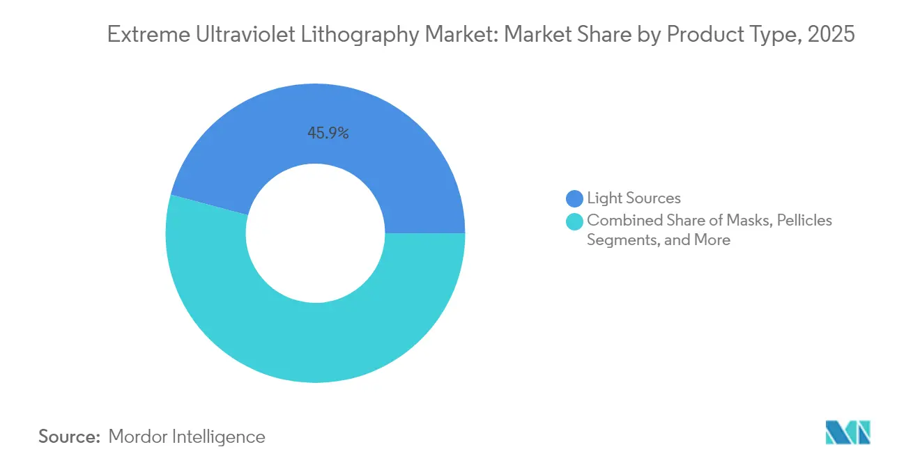
- By product type, Light Sources led with 45.85% of the EUV lithography market share in 2025; pellicles are projected to expand at an 17.9% CAGR through 2031.
- By end-user type, foundries held 52.75% of the EUV lithography market share in 2025, while IDMs are forecast to advance at a 13.6% CAGR to 2031.
- By technology node, the 5 nm class accounted for 33.75% of the EUV lithography market size in 2025; the 2 nm and below node is expected to rise at a 20.2% CAGR between 2026-2031.
- By light-source technology, LPP controlled 87.95% of the EUV lithography market size in 2025; ERL-EUV sources are set to grow at a 26.1% CAGR through 2031.
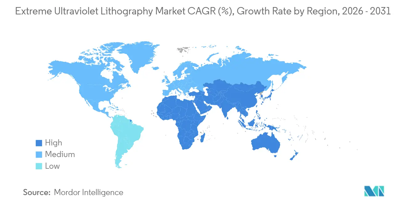
- By geography, Asia-Pacific captured 63.85% revenue share in 2025; the Middle East and Africa region is projected to post an 10.9% CAGR to 2031.
Note: Market size and forecast figures in this report are generated using Mordor Intelligence’s proprietary estimation framework, updated with the latest available data and insights as of 2026.
Global Extreme Ultraviolet Lithography Market Trends and Insights
Drivers Impact Analysis*
| Driver | (~) % Impact on CAGR Forecast | Geographic Relevance | Impact Timeline |
|---|---|---|---|
| Demand for < 5 nm logic and memory nodes | +3.8% | Global, with a concentration in Asia-Pacific | Medium term (2-4 years) |
| Accelerated AI/5G/HPC capacity build-out | +2.4% | North America, Asia-Pacific | Short term (≤ 2 years) |
| Government semiconductor subsidy programs | +1.7% | North America, Europe, Asia-Pacific | Medium term (2-4 years) |
| Transition to High-NA (0.55 NA) EUV platforms | +1.2% | Global | Long term (≥ 4 years) |
| Productivity leap from pellicle membrane breakthroughs | +0.8% | Global | Medium term (2-4 years) |
| ERL-based compact EUV light-source R&D momentum | +0.5% | North America, Asia-Pacific | Long term (≥ 4 years) |
| Source: Mordor Intelligence | |||


Demand for Sub-5 nm Nodes
Mass-production plans for 2 nm chips scheduled for 2025 call for line widths that only EUV exposure can achieve. TSMC has set aside USD 12.3 billion for its EUV tool fleet, a budget that targets 10-15% speed gains or 25-30% power cuts versus 3 nm designs.[1]Techovedas, “TSMC Invests Over USD 12.3 Billion in EUV,” techovedas.com Smartphone and data-center chip buyers have already queued for those nodes, allowing equipment vendors to lock in multi-year backlogs. As a result, the EUV lithography market enjoys a predictable shipment pipeline that mirrors each successive node shrink.
Accelerated AI/5G/HPC Capacity Build-out
AI accelerators, 5G base-band silicon, and high-bandwidth memory all need tight pitch metallization. TSMC’s Q4 2024 revenue rose 37% year-on-year to USD 26.88 billion, illustrating the scale of demand. To keep pace, the company budgeted USD 32-36 billion for capex in 2025, including roughly 60 EUV scanners. Such orders shorten tool lead times and bring smaller suppliers—pellicle, mask blank, and resist vendors—into the growth loop of the EUV lithography market.
Government Semiconductor Subsidy Programs
The U.S. CHIPS Act is funneling USD 52 billion into domestic production, with USD 825 million set aside for an EUV Accelerator in New York. Europe seeks to double its semiconductor share to 20% by 2030, and Japan pairs its subsidy regime with alliances on GAAFET research. These policies tilt capital flows toward new greenfield fabs, broadening the geographical customer base for EUV exposure tools and ancillary components.
Transition to High-NA EUV Platforms
ASML shipped the first 0.55 NA scanner to Intel in late 2023. The platform raises density by 2.9× versus 0.33 NA tools, trimming the number of patterning steps per wafer. Early adopters locked in all units through mid-2025, guaranteeing a multi-year revenue stream. Although each system costs USD 384 million, projected productivity gains offset the purchase by lowering mask count and improving yield.
Restraints Impact Analysis*
| Restraint | (~) % Impact on CAGR Forecast | Geographic Relevance | Impact Timeline |
|---|---|---|---|
| USD 150 m+ system cost and fab retrofit complexity | -3.2% | Global | Medium term (2-4 years) |
| Single-vendor dependency and supply-chain bottlenecks | -2.1% | Global | Short term (≤ 2 years) |
| Stochastic defectivity of EUV photoresists | -1.1% | Global | Medium term (2-4 years) |
| Scarcity of EUV-trained field service engineers | -0.9% | Global, with a concentration in Asia-Pacific | Short term (≤ 2 years) |
| Source: Mordor Intelligence | |||
USD 150 m+ System Cost and Fab Retrofit Complexity
Baseline EUV scanners list at roughly USD 150 million, and high-NA units more than double that figure. Fabs also upgrade clean-room airflow, vibration damping, and power distribution. Smaller foundries struggle to amortize such outlays, risking a technology gap that narrows potential customers for the EUV lithography market. Dual-lane operations, where DUV and EUV run in parallel, further enlarge capital budgets.
Single-Vendor Dependency and Supply-Chain Bottlenecks
ASML owns 100% of the EUV system supply and 90% of the DUV base. Output is capped near 50 tools per year, and export controls restrict shipments to some regions. Critical subsystems—from high-purity glass to multi-layer mirrors—face similar single-source exposure. Any disruption reverberates across the EUV lithography market, prompting governments to invest in domestic component capacity to mitigate risk.
*Our forecasts treat driver/restraint impacts as directional, not additive. The impact forecasts reflect baseline growth, mix effects, and variable interactions.
Segment Analysis
By Product Type: Light Sources Drive Revenue, Pellicles Accelerate Growth
Light sources accounted for 45.85% of the EUV lithography market size in 2025, underscoring their status as the most expensive subsystem in a scanner. Current laser-produced-plasma (LPP) modules convert CO₂-laser pulses and tin droplets into 13.5 nm radiation, but sub-5% conversion efficiency continues to spur research into free-electron alternatives. High average power also drives upgrades such as advanced collector-mirror coatings and debris filters, with service contracts that guarantee power stability, adding annuity revenue for suppliers.
Pellicles are the fastest-growing product, with an 17.9% CAGR projected through 2031. Carbon-nanotube membranes now deliver 97-98% transmittance and withstand 1,000 W exposure, a step change from earlier silicon-nitride films. Major foundries have cleared CNT pellicles for 2 nm process flows, opening a replacement cycle in which every mask layer needs protection; rising scale is already trimming unit cost.


By End-User Type: IDMs Challenge Foundry Dominance
Foundries accounted for 52.75% of the EUV lithography market in 2025 because fab-less customers rely on contract manufacturing. Their specialization lets them order scanners in batches, lock in service capacity, and co-develop processes with tool suppliers. TSMC alone controlled 56% of installed EUV exposure capacity, translating geographic clustering in Taiwan into supply-chain efficiencies and learning-curve cost reductions.
IDMs, however, are expanding faster at a 13.6% CAGR. Intel’s IDM 2.0 model reopens its fabs to external clients while adding High-NA capacity reserved through 2025. Subsidy grants lower its effective capital cost, narrowing the unit-cost gap with pure-play foundries. As IDMs upgrade to gate-all-around transistors, they internalize design-process feedback loops, an advantage that should lift their share of the EUV lithography market over the decade.
By Technology Node: 2 nm and Below Drives Future Growth
The 5 nm node held 33.75% of the EUV lithography market share in 2025, benefiting from mature yields and broad platform support across mobile and datacenter chips. Cost per transistor remains favorable versus 3 nm when productivity bonuses and mask savings are included. Still, roadmaps now center on 2 nm platforms that promise 25-30% energy savings. The segment is forecast to expand at a 20.2% CAGR to 2031, the highest in the hierarchy, as leading customers preload demand for AI and edge-compute processors.
Gate-all-around architectures at 2 nm require tighter overlay control and lower stochastics, both served by EUV’s one-pass imaging. Early pilot lines report line-edge roughness within spec at full-field exposure. Research consortia are fine-tuning high-NA optics and new resists to hold pattern fidelity despite reduced process windows, cementing EUV lithography market relevance for every successive node shrink.

By Light-Source Technology: ERL-EUV Disrupts LPP Dominance
LPP units comprised 87.95% of total shipments in 2025, standardizing the infrastructure of CO₂ lasers, droplet generators, and collector mirrors. Incremental upgrades have nudged average power toward 500 W, enough for most 3 nm mass production. Vendors bundle debris filters to improve mirror life and reduce unscheduled maintenance, bolstering tool utilization across the EUV lithography market.
ERL-EUV platforms, projected to clock a 26.1% CAGR, eliminate tin debris by generating coherent EUV in a superconducting linac. Lawrence Livermore research indicates 2 kW output at 0.33 GeV beam energies, slashing wall-plug power draw. Prototype timelines align with the industry’s 1.4 nm node, giving chipmakers an alternative that could diversify supply. If commercialized, ERL technology would lower operating costs and environmental footprint, two priorities for subsidy-backed green fabs.
Geography Analysis
Asia-Pacific led the EUV lithography market with 63.85% of 2025 revenue. Taiwan’s TSMC alone has installed roughly 60 scanners financed by the USD 12.3 billion EUV budget noted above. Samsung’s Korean fabs will bring their first High-NA tool online in Q1 2025. Japanese suppliers such as Hoya remain the primary source of EUV mask blanks, further reinforcing regional clustering.
North America is gaining momentum. The CHIPS Act earmarks USD 825 million for an EUV Accelerator in Albany, while Intel’s High-NA roll-out benefits from early access to all first-wave scanners. Department of Energy grants fund next-generation light-source research at Lawrence Livermore National Laboratory, positioning the region as an innovation hub.
The Middle East and Africa region, although starting from a small base, is forecast to grow at an 10.9% CAGR to 2031 as sovereign wealth funds in the UAE and Saudi Arabia invest in AI infrastructure that will ultimately require advanced chip supply. Early memoranda with U.S. tool vendors cover pilot fabs and clean-room engineering, leaving open a path to EUV adoption once ecosystems mature.

Competitive Landscape
Market concentration is extreme, as ASML is the sole supplier of EUV scanners after investing USD 9 billion in cumulative R&D. Scanner prices rose 22% between 2020 and 2022, reflecting strong demand and limited capacity. Closed co-development loops tie ASML to Zeiss SMT for optics and to Cymer for light sources, while multiyear purchase agreements allocate supply among TSMC, Samsung, and Intel.
Component makers target adjacent niches: Zeiss adds adaptive mirror stages, chemical suppliers refine metal-oxide resists, and Imec hosts pilot-line testing under a five-year pact with ASML.[4]Imec, “Imec and ZEISS Sign New Strategic Partnership Agreement,” imec-int.com U.S. CHIPS Act funding expands Corning’s ultra-low-expansion glass output, easing a mirror-blank bottleneck.
Geopolitics also reshapes demand. Export controls restrict latest-generation scanners from select Chinese fabs, prompting domestic alternatives and parallel DUV investments. European and U.S. policymakers answer with regional tool ecosystems, and the five-year ASML–Imec partnership formalizes knowledge sharing while pursuing sustainability goals. Over the medium term, EUV supply is likely to remain single-sourced, yet emerging light-source and pellicle vendors could fragment adjacent segments.
Extreme Ultraviolet Lithography Industry Leaders
-
ASML Holding NV
-
ZEISS SMT
-
Gigaphoton Inc.
-
Cymer LLC
-
Canon Inc.
- *Disclaimer: Major Players sorted in no particular order


Recent Industry Developments
- May 2025: ASML unveiled plans for its next-generation Hyper-NA extreme ultraviolet lithography technology, extending its roadmap beyond current High-NA systems.
- April 2025: ASML reported €7.7 billion in Q1 2025 net sales, citing AI demand as a growth catalyst.
- March 2025: ASML and imec signed a five-year strategic partnership to advance semiconductor R&D using 0.55 NA and 0.33 NA EUV tools.
- March 2025: Imec and ZEISS extended their collaboration to 2029 to enhance the NanoIC pilot line for sub-2 nm research.


Research Methodology Framework and Report Scope
Market Definitions and Key Coverage
Our study defines the extreme ultraviolet (EUV) lithography market as the worldwide revenue generated from newly built EUV scanners and their integral light sources, mirrors, masks, pellicles, and related sub-assemblies that enable patterning at 7 nm nodes and below. These sales are counted at the point the original equipment manufacturer books revenue to foundries or integrated device manufacturers.
Scope exclusions: After-sales service contracts, refurbished deep-ultraviolet platforms, and in-house tool conversions are not part of this market.
Segmentation Overview
-
By Product Type
- Light Sources
- Mirrors / Optics
- Masks
- Pellicles
- Mask Blanks
-
By End-User Type
- Foundries
- Integrated Device Manufacturers (IDMs)
-
By Technology Node
- 7 nm and above
- 5 nm
- 3 nm
- 2 nm and below
-
By Light-Source Technology
- Laser-Produced Plasma (LPP)
- Gas-Discharge Plasma
- Vacuum Spark
- ERL-EUV
-
By Geography
-
North America
- United States
- Canada
-
South America
- Brazil
- Rest of South America
-
Europe
- Germany
- Netherlands
- United Kingdom
- France
- Italy
- Russia
- Rest of Europe
-
Asia-Pacific
- Taiwan
- South Korea
- Japan
- China
- Singapore
- Rest of Asia-Pacific
-
Middle East and Africa
-
Middle East
- GCC
- Turkey
- Saudi Arabia
- Rest of Middle East
-
Africa
- South Africa
- Rest of Africa
-
Middle East
-
North America
Detailed Research Methodology and Data Validation
Primary Research
We held structured discussions with Asia-Pacific process engineers, European IDM procurement leads, and North American equipment distributors. Their insights on installation lead times, usable throughput, and expected high-NA slots closed documentary gaps and refined the cost curves anchoring our revenue model.
Desk Research
We began with open data such as SEMI shipment statistics, World Fab Forecast updates, customs codes for photolithography tools, and patent streams accessed through Questel that trace high-NA optics. Academic articles in IEEE Transactions on Semiconductor Manufacturing and news archived on Dow Jones Factiva added technical depth, while Mordor Intelligence paid databases like D&B Hoovers helped verify supplier financials.
Our team then reviewed 10-K filings, investor day slide decks, and subsidy disclosures under the US CHIPS and European Chips Acts to match announced wafer-fab capacity with tool backlogs, strengthening price and volume bands before primary work. The sources listed are illustrative; many additional reputable documents were consulted to cross-check figures and clarify scope.
Market-Sizing & Forecasting
A top-down build starts with global 300 mm capacity additions, scanner order logs, and average selling prices, which are then checked by selective bottom-up roll-ups from sampled suppliers and channel evidence. Key variables include new fab start counts, node transition timing, scanner ASP erosion, numerical-aperture upgrades, subsidy disbursements, and AI data-center demand. Forecasts employ multivariate regression combined with scenario analysis to show how memory inventory swings or fiscal incentives steer tool demand through 2030. Divergences between approaches are calibrated using primary feedback.
Data Validation & Update Cycle
Every model passes variance testing against historical SEMI billings and import patterns, followed by a two-step peer review. Any outlier over five percent triggers expert re-contact. Mordor analysts refresh data annually and issue interim updates when material events, like a delayed high-NA shipment, occur, with a final validation pass just before publication.
Why Mordor's EUV Lithography Baseline Commands Reliability
Published estimates differ because firms choose distinct scopes, price decks, and refresh cadences.
We acknowledge those gaps upfront, then show how our disciplined variable selection delivers a dependable baseline.
Benchmark comparison
| Market Size | Anonymized source | Primary gap driver |
|---|---|---|
| USD 23.71 B (2025) | Mordor Intelligence | |
| USD 12.16 B (2025) | Global Consultancy A | Excludes light-source revenue and books value only at factory acceptance |
| USD 10.16 B (2024) | Trade Journal B | Limits geography to Asia-Pacific and applies aggressive ASP deflation |
| USD 12.18 B (2024) | Market Insights Firm C | Omits mirror and pellicle subsystems and uses fixed 2021 exchange rates |
The comparison shows that when scope is narrow or price assumptions outdated, totals fall well below the balanced figure our analysts derive. By tracing every input to transparent variables and revisiting them on a set schedule, Mordor Intelligence gives decision-makers a market baseline they can trust.


Key Questions Answered in the Report
What is the current size and growth outlook of the EUV lithography market?
The market is valued at USD 25.93 billion in 2026 and is projected to reach USD 40.54 billion by 2031, reflecting a 9.35% CAGR.
Which product segment is expected to grow the fastest through 2031?
Pellicles, driven by carbon-nanotube membranes, show the highest momentum with an 17.9% CAGR forecast for 2026-2031.
How do High-NA scanners affect capital budgets?
Each 0.55 NA tool costs about USD 384 million, more than double standard EUV units, but boosts transistor density 2.9×, reducing multi-patterning and long-run wafer cost.
Which geography leads demand, and which region is expanding quickest?
Asia-Pacific controls 63.85% of 2025 revenue, while the Middle East and Africa region is set to rise at an 10.9% CAGR to 2031 as new tech investments gain traction.
What are the primary barriers to wider EUV adoption?
High system price and fab retrofit complexity (-3.2% impact on forecast CAGR) and single-vendor dependency (-2.1% impact) are the most significant hurdles.
Page last updated on:


