Electron Microscope Market Size and Share
Market Overview
| Study Period | 2020 - 2031 |
|---|---|
| Market Size (2026) | USD 5.28 Billion |
| Market Size (2031) | USD 7.82 Billion |
| Growth Rate (2026 - 2031) | 8.20% CAGR |
| Fastest Growing Market | Asia Pacific |
| Largest Market | North America |
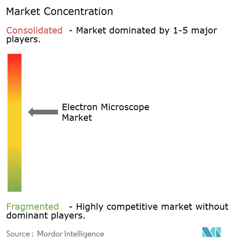
| Market Concentration | Medium |
Major Players *Disclaimer: Major Players sorted in no particular order Image © Mordor Intelligence. Reuse requires attribution under CC BY 4.0. | |
Electron Microscope Market Analysis by Mordor Intelligence
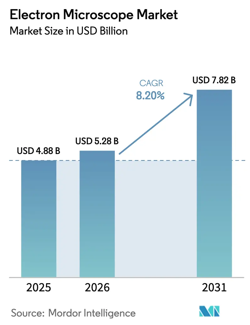
The Electron Microscope Market size is projected to be USD 4.88 billion in 2025, USD 5.28 billion in 2026, and reach USD 7.82 billion by 2031, growing at a CAGR of 8.20% from 2026 to 2031.
As sub-3nm gate-all-around logic transitions into pilot and early production, demand is increasing. This development is driving fabs to expand the adoption of transmission electron microscopes for atomic-resolution defect localization. At the same time, scanning electron microscopes remain the preferred choice for high-throughput inspections and biological screenings. Advancements in artificial intelligence have shifted microscope control from manual to automated, significantly reducing cryo-EM data collection cycles from days to hours and improving overnight utilization. National initiatives in China and India are focusing on building domestic capacity in electron optics to reduce dependency on export licenses and shorten lead times. This shift is fragmenting a supply chain that was traditionally centered in Japan, Germany, and the United States. Competitive positioning is increasingly leaning toward software-defined throughput as industry players incorporate machine-learning modules. Additionally, focused-ion-beam SEM and correlative light-electron workflows are creating new opportunities in advanced packaging and cell biology.
Key Report Takeaways
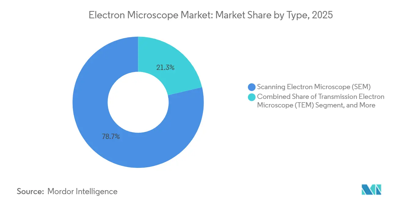
- By instrument type, SEM held 78.7% of the electron microscope market share in 2025, and TEM is projected to grow at an 11.8% CAGR through 2031.
- By application, life sciences and biology accounted for 24.8% of the market in 2025, and nanotechnology is forecast to expand at a 9.4% CAGR through 2031.
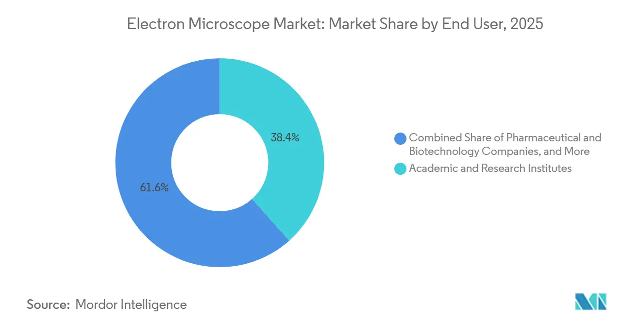
- By end user, academic and research institutes accounted for 38.4% of spending in 2025, and pharmaceutical and biotechnology companies are projected to grow at a 10.1% CAGR through 2031.
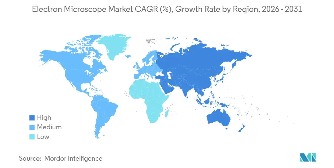
- By geography, North America captured 41.1% of the electron microscope market share in 2025, and Asia-Pacific is projected to grow at an 11.6% CAGR through 2031.
Note: Market size and forecast figures in this report are generated using Mordor Intelligence’s proprietary estimation framework, updated with the latest available data and insights as of 2026.
Global Electron Microscope Market Trends and Insights
Drivers Impact Analysis*
| DRIVER | (~) % IMPACT ON CAGR FORECAST | GEOGRAPHIC RELEVANCE | IMPACT TIMELINE |
|---|---|---|---|
| Rising demand for high-magnification & high-resolution imaging | +1.5% | APAC core, spill-over to MEA | Long term (≥ 4 years) |
| Expansion of nanotechnology research & advanced materials programs | +1.3% | North America & EU, expanding to APAC | Medium term (2-4 years) |
| Sub-5nm semiconductor node adoption driving failure-analysis demand | +2.1% | Global, concentrated in Taiwan, South Korea, U.S. | Medium term (2-4 years) |
| AI-enabled automated TEM/SEM workflows cutting analysis time | +1.8% | Global, early gains in North America & EU | Short term (≤ 2 years) |
| National TEM-manufacturing initiatives in China & India are easing import barriers | +1.5% | APAC core, spill-over to MEA | Long term (≥ 4 years) |
| Cryo-electron tomography convergence with spatial multi-omics in drug discovery | +1.3% | North America & EU, expanding to APAC | Medium term (2-4 years) |
| Source: Mordor Intelligence | |||
Sub-5nm Semiconductor Node Adoption Driving Failure-Analysis Demand
The transition to sub-5nm nodes is driving growth in the electron microscope market, as optical metrology struggles to address line-edge roughness, stochastic dopant variation, and interfacial oxide defects. TSMC's 2nm pilot operations highlight the increasing need for cross-sectional imaging, fueled by gate-all-around nanosheet architectures. Multiple TEMs per cleanroom module are now utilized to ensure channel uniformity and contact resistance at atomic resolution. Samsung Foundry's planned 2025 investment emphasizes plasma-focused-ion-beam SEM, reflecting the demand for high-throughput lamella preparation on brittle low-k materials while minimizing beam damage.[1]Samsung Foundry, “Advanced Process Technology,” Samsung, samsung.com Distributed failure analysis is gaining traction as next-generation United States fabs expand on-site TEM service capacity to accelerate yield-learning loops and reduce shipping delays.
AI-Enabled Automated TEM/SEM Workflows Cutting Analysis Time
Machine learning is now integrated across the acquisition stack, enabling autonomous grid selection, defocus control, and particle-orientation classification. These advancements facilitate unattended cryo-EM runs, reducing project timelines and improving asset utilization. Thermo Fisher's SmartEM software, launched in December 2025, leverages convolutional neural networks trained on a vast dataset of micrographs to optimize imaging conditions and eliminate ice-contaminated regions, increasing throughput by 40% without requiring hardware upgrades.[2]Thermo Fisher Scientific, “SmartEM Software Overview,” Thermo Fisher, thermofisher.com JEOL's AI-powered auto-tuning for its 300kV TEM platforms uses reinforcement learning to achieve Scherzer defocus in under three minutes, significantly enhancing the daily screening capacity for protein constructs. Hitachi's SU9600 field-emission SEM incorporates edge-detection logic that adjusts scan speed and beam current during high-aspect-ratio scans, preventing charge build-up that could distort nanowire metrology.
National TEM-Manufacturing Initiatives in China & India Easing Import Barriers
China's Ministry of Industry and Information Technology has allocated significant funding in 2025 to support domestic production of 200kV and 300kV TEM columns, aiming to reduce reliance on foreign suppliers. State-sponsored prototype systems are narrowing the gap with high-end platforms, achieving 0.8-angstrom information limits on lattice imaging, with ongoing improvements in corrector stability and detector quantum efficiency. In 2024, India introduced a co-investment initiative to establish regional TEM fabrication hubs, including collaborations for column assembly and technician training in key cities. These efforts expand purchasing options for universities and mid-tier labs facing lengthy export-license processes, although high-end structural biology and advanced-node metrology continue to favor imported flagship models.
Cryo-Electron Tomography Convergence with Spatial Multi-Omics in Drug Discovery
Pharmaceutical companies are integrating cryo-electron tomography with spatial transcriptomics and proteomics to map protein complexes in native cellular environments, validating target accessibility before advancing screening campaigns. Pfizer's 2025 acquisition of a Titan Krios G4 enhances its in-house capabilities for determining the structures of antibody-drug conjugates, reducing reliance on external facilities and accelerating lead-optimization cycles. In 2024, Moderna adopted Glacios cryo-TEMs to analyze lipid nanoparticle morphology and mRNA encapsulation, linking particle structure to in vivo transfection rates to refine formulations.
Restraint Impact Analysis*
| RESTRAINT | (~) % IMPACT ON CAGR FORECAST | GEOGRAPHIC RELEVANCE | IMPACT TIMELINE |
|---|---|---|---|
| High capital & lifetime maintenance costs | -1.4% | Global | Long term (≥ 4 years) |
| Global helium shortage inflating cryo-EM operating expenditure | -0.9% | Global, acute in North America & EU | Short term (≤ 2 years) |
| Shortage of skilled electron-microscopy personnel | -0.4% | Global | Long term (≥ 4 years) |
| Export-control restrictions on advanced dual-use instrumentation | -6.7% | Global | Short term (≤ 2 years) |
| Source: Mordor Intelligence | |||
High Capital & Lifetime Maintenance Costs
Aberration-corrected TEM systems, featuring monochromators and direct-electron detectors, are priced between USD 4 million and USD 7 million. Additionally, annual services, cryogens, and controlled-environment infrastructure add an extra USD 300,000 to USD 500,000 to the total ownership cost. Smaller universities and contract-research providers often opt for mid-tier 120kV cryo-TEMs, priced around USD 2 million, to balance resolution with budget limitations. Core facilities and leasing schemes assist in pooling capital and utilization; however, challenges such as instrument scheduling and the need for specialized training continue to limit throughput in the electron microscope market.
Global Helium Shortage Inflating Cryo-EM Operating Expenditure
In the United States, liquid-helium spot prices increased from USD 8 per liter in early 2024 to USD 18 per liter by late 2025 due to supply disruptions. This rise effectively doubled the annual cryogen budget for a 300kV cryo-TEM, increasing it from USD 50,000 to USD 100,000. Laboratories have responded by rationing uptime and prioritizing fee-paying users, which risks reducing hands-on exposure for trainees in microscopy programs across the electron microscope market. Closed-cycle helium-recovery systems, capable of capturing over 95% of boil-off gas, cost approximately USD 150,000 and require compressor maintenance. However, with a payback period of just two years at current prices, these systems have become standard in new cryo-EM suites.
*Our forecasts treat driver/restraint impacts as directional, not additive. The impact forecasts reflect baseline growth, mix effects, and variable interactions.
Segment Analysis
By Type: TEM Gains as Cryo-Biology and Sub-Angstrom Metrology Converge
In 2025, scanning electron microscopes captured a dominant 78.7% of the electron microscope market, driven by affordability and versatility in semiconductor inspections, biological screenings, and electronics failure analyses. As cryo-EM becomes critical in structure-based drug design and advanced-node fabs require sub-angstrom lattice imaging for epitaxial stack validation, transmission electron microscopes are expected to grow at an 11.8% CAGR through 2031. SEMs remain the preferred choice for in-line process control due to their speed, simple sample preparation, and robust automation, aligning with the market's throughput objectives. TEMs are increasingly essential in root-cause analysis, where atomic-resolution defect and interface mapping is vital for yield learning at 3nm and below. The development of dual-beam FIB-SEM, particularly with xenon plasma sources, enhances 3D circuit reconstruction and advanced-packaging failure analysis, supporting both SEM throughput and TEM cross-sectional validation.


By Application: Nanotechnology Accelerates as Quantum Materials Enter Pilot Production
In 2025, life sciences and biology accounted for a 24.8% share of the electron microscope market, driven by the integration of cryo-EM into structural biology, cellular tomography, and virology in core facilities and pharmaceutical laboratories. Nanotechnology, fueled by the demand for atomic-scale structure and composition maps in two-dimensional materials, quantum dots, and engineered metamaterials, is the fastest-growing application, with a 9.4% CAGR through 2031. The electronics and semiconductor sectors generate the highest revenue, utilizing wafer-scale SEM inspections and TEM-based analyses at sub-5nm nodes and in advanced packaging. Material science, including metallurgy, ceramics, and polymers, increasingly adopts EBSD and correlative analyses to support lightweighting initiatives in aerospace and automotive sectors. In forensics, SEM-EDS is increasingly used for analyzing gunshot residues and trace evidence, adhering to standardized methods and reporting frameworks.
By End User: Pharmaceutical and Biotechnology Companies Internalize Cryo-EM to Shorten Discovery Cycles
In 2025, academic and research institutions accounted for 38.4% of end-user spending, reflecting the importance of multi-user core facilities that consolidate capital and offer training, scheduling, and fee-for-service access across departments. Pharmaceutical and biotechnology companies are projected to grow at a 10.1% CAGR through 2031 as they adopt cryo-EM in-house, streamlining structure-based designs and reducing reliance on external services. Semiconductor and electronics manufacturers are driving strong demand for SEM and TEM to support yield enhancements at new fabs in Taiwan, South Korea, and the United States. Partnerships between academia and industry, emphasizing access and co-authorship, are becoming more common, facilitating capital cost distribution while safeguarding proprietary datasets for drug development programs. In regulated environments, compliance requirements, such as maintaining audit trails for automated decisions, influence vendor selection for pharmaceutical laboratories.
Geography Analysis
In 2025, North America accounted for 41.1% of the electron microscope market share, driven by initiatives such as National Institutes of Health cryo-EM centers and semiconductor R&D hubs. These hubs, along with biopharma clusters, focus on structure-based discovery. As advanced-node ramps progress, semiconductor programs in Oregon, Arizona, and Ohio are expanding on-site metrology capacity. Tool vendors and materials suppliers are strategically positioning applications labs near leading-edge fabs to accelerate development cycles and support joint process integration. Academic core facilities in Boston and the Bay Area anchor community-access programs, consolidating resources for cryo-EM and FIB-SEM training. Additionally, regulatory clarity on data traceability and validation is enabling broader adoption of AI-enabled modules in regulated labs.
Asia-Pacific is projected to grow at an 11.6% CAGR through 2031, fueled by fab construction in Taiwan and South Korea and government co-investment in domestic electron-optics manufacturing in China and India. TSMC’s advanced-node roadmaps and Samsung Foundry’s expansions are driving demand for high-throughput SEM and atomic-resolution TEM for process debugging. India’s co-investment programs focus on domestic assembly and technician training to diversify supply chains and reduce delivery times. Local universities across the region are enhancing cryo-EM capacity to support the biotech ecosystem, thereby increasing the diversity of applications in the electron microscope market. Export-control regimes are shaping technology flows, encouraging selective onshore manufacturing and localized service models.
Europe maintains steady demand across materials science, automotive, and aerospace sectors as programs at the Max Planck Society and Fraunhofer Institutes expand EBSD and correlative workflows. However, public budget constraints are tempering growth, making shared-access models and multi-institution consortia more attractive. In the Middle East and Africa, Gulf research universities are investing in cryo-TEM and FIB-SEM to build scientific capacity beyond hydrocarbons. South America, while the smallest regional segment, is seeing Brazil’s nanotechnology initiatives and Argentina’s CONICET upgrades improve access to modern electron optics.

Competitive Landscape
Thermo Fisher Scientific, JEOL, Hitachi High-Tech, and Carl Zeiss dominate the electron microscope market, collectively accounting for nearly 65% of the revenue. Meanwhile, niche players like Nion and Delmic are carving out their space, focusing on aberration-corrected STEM and correlative light-electron workflows. Leading companies are shifting their differentiation strategy, transitioning from a sole emphasis on hardware to a more integrated software approach. By embedding machine learning, they are enhancing throughput and ensuring consistency across diverse user bases. Their new feature roadmaps emphasize automated alignment, aberration correction, contamination detection, and scan-parameter control. These advancements promise improved stability for a wide range of samples in the electron microscope market.
There is a notable opportunity in mid-tier cryo-TEMs priced between USD 1.5 million and USD 2.5 million. These instruments cater to smaller biotech firms and CROs, striking a balance between resolution and cost. Multi-beam SEM arrays are revolutionizing wafer inspections. By parallelizing the process, they alleviate bottlenecks in high-volume manufacturing, shifting the criteria for adoption from a mere field of view to sustained throughput. While software subscription models for analytics and automation are on the rise, many buyers still lean toward capital purchases, valuing the flexibility these assets offer. Service models are evolving, with on-site support at mega-fabs becoming increasingly popular. This trend is driven by fabs' desire to expedite failure-analysis loops. Sustainability is becoming a pivotal consideration, particularly in features such as helium recovery. Such factors are gaining prominence, particularly for cryo-EM fleets operating in shared facilities.
Electron Microscope Industry Leaders
ADVANTEST CORPORATION
Hitachi High-Tech Corporation (Hitachi, Ltd.)
JEOL Ltd.
Thermo Fisher Scientific Inc.
Carl Zeiss AG
- *Disclaimer: Major Players sorted in no particular order

Recent Industry Developments
- January 2026: Hitachi High-Tech Corporation launched the HT7800II 120kV TEM optimized for biological and polymer imaging, incorporating a CMOS camera and streamlined user interface to lower the barrier for entry-level users.
- October 2025: Hitachi High-Tech Corporation introduced the Ultrahigh-Resolution Scanning Electron Microscope SU9600, designed for precise observations at the sub-nano level. The SU9600 maintains industry-leading resolution standards while incorporating automated features to enhance data acquisition efficiency.
- July 2025: Thermo Fisher Scientific plans to introduce two new electron microscopes at the Microscopy & Microanalysis (M&M) event in Salt Lake City, Utah, from July 27-31, aiming to advance the accessibility of scientific research.
- March 2025: Shimadzu Corporation, following its partnership with TESCAN GROUP from Czechia, a leading scanning electron microscope manufacturer, has launched the “SUPERSCAN SS-4000” model in Japan under the joint brand “Shimadzu by TESCAN.”


Global Electron Microscope Market Report Scope
As per the scope of the report, an electron microscope is a microscope that uses a beam of accelerated electrons as a source of illumination, and this technique is known as electron microscopy (EM). Electron microscopes aid in obtaining high-resolution images of biological and non-biological specimens by controlled use of electrons in a vacuum captured on a phosphorescent screen. The electron microscope market is segmented by type, application, and geography.
The market is segmented by type, application, and geography. By type, the market is segmented into transmission electron microscope (TEM), scanning electron microscope (SEM), and others. By application, the market is segmented into electronics and semiconductors, life sciences and biology, material science, nanotechnology, and other applications. By geography, the market is segmented into North America, Europe, Asia-Pacific, Middle-East and Africa, and South America. The market report also covers the estimated market sizes and trends for 17 different countries across major regions globally. The report offers market size and forecasts in value (USD) for the above segments.
| Transmission Electron Microscope (TEM) |
| Scanning Electron Microscope (SEM) |
| Dual-Beam (FIB-SEM) |
| Others (REM, Low-Voltage EM) |
| Electronics & Semiconductors |
| Life Sciences & Biology |
| Material Science |
| Nanotechnology |
| Forensic Science |
| Energy & Battery Research |
| Others |
| Academic & Research Institutes |
| Semiconductor & Electronics Manufacturers |
| Pharmaceutical & Biotechnology Companies |
| Industrial QA/QC Labs |
| Government & Defense Laboratories |
| Others |
| North America | United States |
| Canada | |
| Mexico | |
| Europe | Germany |
| United Kingdom | |
| France | |
| Italy | |
| Spain | |
| Rest of Europe | |
| Asia-Pacific | China |
| India | |
| Japan | |
| Australia | |
| South Korea | |
| Rest of Asia-Pacific | |
| Middle East and Africa | GCC |
| South Africa | |
| Rest of Middle East and Africa | |
| South America | Brazil |
| Argentina | |
| Rest of South America |
| By Type | Transmission Electron Microscope (TEM) | |
| Scanning Electron Microscope (SEM) | ||
| Dual-Beam (FIB-SEM) | ||
| Others (REM, Low-Voltage EM) | ||
| By Application | Electronics & Semiconductors | |
| Life Sciences & Biology | ||
| Material Science | ||
| Nanotechnology | ||
| Forensic Science | ||
| Energy & Battery Research | ||
| Others | ||
| By End User | Academic & Research Institutes | |
| Semiconductor & Electronics Manufacturers | ||
| Pharmaceutical & Biotechnology Companies | ||
| Industrial QA/QC Labs | ||
| Government & Defense Laboratories | ||
| Others | ||
| By Geography | North America | United States |
| Canada | ||
| Mexico | ||
| Europe | Germany | |
| United Kingdom | ||
| France | ||
| Italy | ||
| Spain | ||
| Rest of Europe | ||
| Asia-Pacific | China | |
| India | ||
| Japan | ||
| Australia | ||
| South Korea | ||
| Rest of Asia-Pacific | ||
| Middle East and Africa | GCC | |
| South Africa | ||
| Rest of Middle East and Africa | ||
| South America | Brazil | |
| Argentina | ||
| Rest of South America | ||


Key Questions Answered in the Report
What is the electron microscope market size in 2026 and what is the 2031 outlook?
The electron microscope market size is USD 5.28 billion in 2026 and is expected to reach USD 7.82 billion by 2031 at an 8.2% CAGR.
Which instrument type is largest and which is growing fastest?
SEM leads with 78.7% revenue share in 2025, while TEM is projected to grow fastest at an 11.8% CAGR through 2031.
Which application areas are most important in 2026?
Life sciences and biology hold the largest share by application, while nanotechnology is the fastest-growing at a 9.4% CAGR through 2031.
Who are the leading companies shaping the electron microscope industry today?
Thermo Fisher Scientific, JEOL, Hitachi High-Tech, and Carl Zeiss lead, with specialists such as Nion and Delmic active in niche high-resolution and correlative workflows.
Which region accounts for the largest share and which will expand fastest?
North America holds 41.1% share in 2025, while Asia-Pacific is projected to expand fastest at an 11.6% CAGR through 2031.
What factors are accelerating adoption in semiconductors and biopharma?
Sub-5nm node metrology, AI-enabled automation, and wider cryo-EM deployment in drug discovery are the primary drivers across both end markets.
Page last updated on:


