Microscopy Device Market Size and Share
Market Overview
| Study Period | 2020 - 2031 |
|---|---|
| Market Size (2026) | USD 10.82 Billion |
| Market Size (2031) | USD 14.32 Billion |
| Growth Rate (2026 - 2031) | 5.76% CAGR |
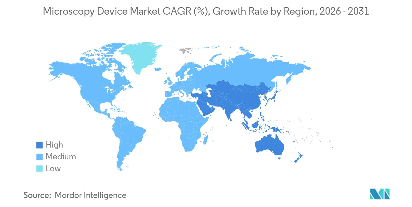
| Fastest Growing Market | Asia-Pacific |
| Largest Market | North America |
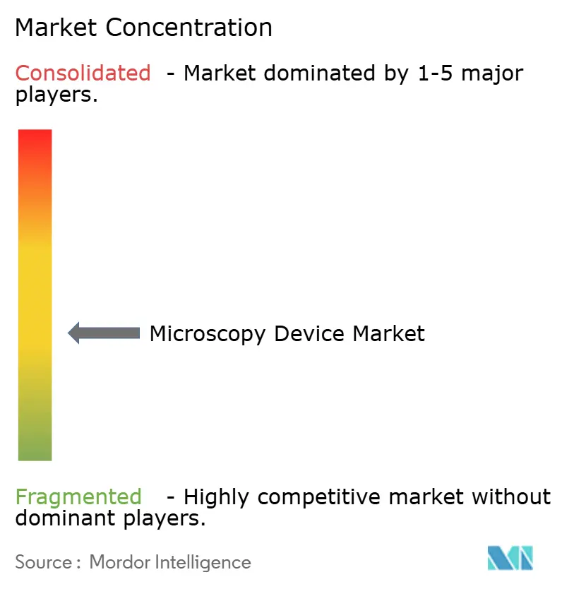
| Market Concentration | Medium |
Major Players *Disclaimer: Major Players sorted in no particular order Image © Mordor Intelligence. Reuse requires attribution under CC BY 4.0. | |
Microscopy Device Market Analysis by Mordor Intelligence
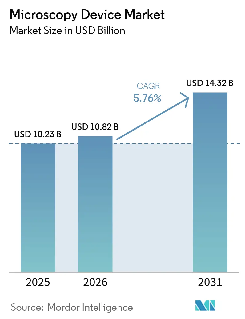
The Microscopy Device Market size is projected to be USD 10.23 billion in 2025, USD 10.82 billion in 2026, and reach USD 14.32 billion by 2031, growing at a CAGR of 5.76% from 2026 to 2031.
Growth reflects three linked shifts, including gate-all-around transistor roadmaps that demand sub-nanometer metrology in semiconductor fabs, the spread of desktop cryogenic electron microscopy for structure-based drug discovery, and AI-augmented digital pathology replacing manual slide reading in hospitals and labs. On the product front, optical systems maintained the most extensive installed base due to clinical and educational volumes, while electron microscopy is gaining share as lower-priced cryo-EM systems reach mid-tier institutions. Competitive intensity remains high as leading vendors integrate software and consumables to lock in workflows while specialist players target high-value niches.
Key Report Takeaways
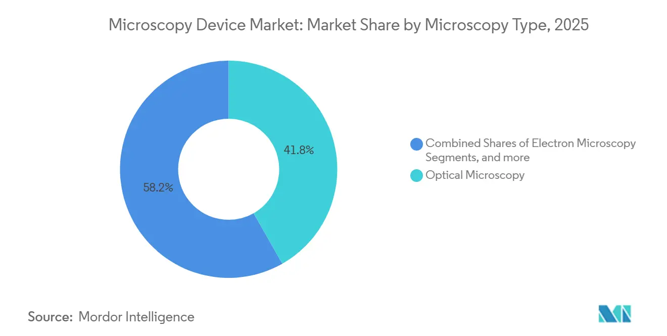
- By microscopy type, optical microscopy led with 41.78% revenue share in 2025; electron microscopy is forecast to expand at a 6.56% CAGR to 2031.
- By application, life science accounted for a 34.08% share in 2025; nanotechnology research is projected to grow at a 6.59% CAGR through 2031.
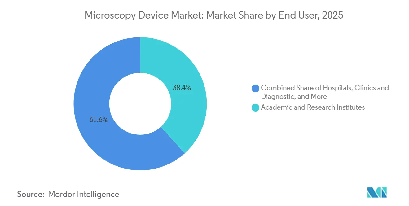
- By end user, academic and research institutes accounted for 38.35% of revenue in 2025; hospitals, clinics, and diagnostic labs are set to record the highest CAGR of 6.60% through 2031.
- By geography, North America held a 39.25% revenue share in 2025; Asia-Pacific is forecast to grow at a 6.74% CAGR through 2031.
Note: Market size and forecast figures in this report are generated using Mordor Intelligence’s proprietary estimation framework, updated with the latest available data and insights as of 2026.
Global Microscopy Device Market Trends and Insights
Drivers Impact Analysis*
| DRIVER | (~) % IMPACT ON CAGR FORECAST | GEOGRAPHIC RELEVANCE | IMPACT TIMELINE |
|---|---|---|---|
| Technological advancements in super-resolution optics & quantum sensing | +1.2% | Global, with early adoption in North America & Europe | Medium term (2-4 years) |
| AI-driven automated digital pathology adoption | +1.4% | North America & Europe, expanding to APAC | Short term (≤ 2 years) |
| Government nanotech & life-science R&D funding surge | +1.0% | Global, concentrated in U.S., EU, China | Long term (≥ 4 years) |
| Semiconductor gate-all-around node miniaturization needs | +0.9% | APAC core (Taiwan, South Korea), spill-over to North America | Medium term (2-4 years) |
| Desktop cryo-em democratizing structure-based drug design | +0.7% | North America & Europe, emerging in APAC | Medium term (2-4 years) |
| Sustainability push for energy-efficient, modular microscopes | +0.4% | Europe & North America, regulatory-driven | Long term (≥ 4 years) |
| Source: Mordor Intelligence | |||


Technological Advancements in Super-Resolution Optics & Quantum Sensing
Super-resolution techniques like STED, SIM, and PALM are breaking the diffraction barrier to reveal structures below 50 nanometers, which strengthens single-cell and neurodegeneration research as labs push to quantify protein interactions in living systems. Early adopters are layering quantum sensing based on nitrogen-vacancy centers in diamond to image magnetic fields, detect nanoscale defects in semiconductor wafers, and capture single-molecule events in biophysics. The microscopy device market is benefiting as buyers seek hybrid platforms that switch among widefield, confocal, and super-resolution modes within the same workflow to maximize throughput. Academic consortia and pharmaceutical companies in North America and Europe are leading purchases due to pipeline demands for target validation and high-content screening. Complexity in optical alignment and reliance on specific fluorophores still slow routine clinical use, creating a service and training opportunity for vendors with robust application support.
AI-Driven Automated Digital Pathology Adoption
Pathology networks are moving from manual microscopy to whole-slide imaging combined with convolutional neural networks that classify tissue, quantify biomarkers, and flag anomalies, and several models now show sensitivities exceeding 95% in indications with strong ground truth. In January 2026, the Central Silk Board in India highlighted an AI-enabled microscope initiative that helps farmers detect silkworm disease earlier, underscoring how applied AI microscopy is expanding beyond clinical settings into production environments. Oncology workloads are a catalyst because tumor microenvironment analysis requires quantifying immune infiltrates and vascular structures across gigapixel images at scale. The European Union’s In Vitro Diagnostic Regulation mandates CE marking for AI-based diagnostic software, prompting vendors to run prospective clinical validation studies to align model performance with clinical endpoints.[1]European Commission, “In Vitro Diagnostic Regulation Overview,” European Commission, ec.europa.eu Hospitals and diagnostic labs are the fastest-growing end-user segment at a 6.60% CAGR through 2031, driven by pathologist labor constraints and the need to standardize multi-site interpretations to reduce variability in care
Government Nanotech & Life-Science R&D Funding Surge
Public investment rose to record levels in 2025, as the U.S. National Institutes of Health budgeted USD 47.5 billion, including line items for structural biology and advanced imaging, which supported upgrades across national centers and university cores. The U.S. National Science Foundation’s Mid-scale Research Infrastructure programs fund equipment in the USD 4 million to USD 100 million range, which supports regional cryo-EM hubs and multi-user facilities that pool operating budgets.[2]National Institutes of Health, “NIH Budget FY2025,” NIH, nih.gov
The European Research Council’s Synergy Grants, funded in 2025, supported 66 projects focused on quantum biology and single-molecule science, with awards up to EUR 10 million (USD 10.7 million) over six years, thereby expanding procurement of top-end optical and electron platforms.[3]European Research Council, “Synergy Grants 2025 Results,” ERC, erc.europa.eu These flows reinforced the position of academic and research institutes, which held the largest end-user share in 2025 and continued to influence instrument specification roadmaps for next-generation systems. The long-run effect depends on continuity in grant cycles and refresh intervals as agencies weigh distributed funding against a few flagship facilities.
Semiconductor Gate-All-Around Node Miniaturization Needs
Gate-all-around transistor architectures at and below the 2-nanometer node intensify demand for high-resolution TEM and SEM to resolve inner spacer voids and nanosheet thickness variations that optical metrology misses. Samsung reported using dozens of inline SEMs and metrology upgrades for process development, suggesting rising tool counts and higher utilization rates for electron-beam inspection. The microscopy device market benefits as fabs extend metrology coverage to more layers and increase sampling to control yield in logic and memory ramps. Asia-Pacific manufacturers lead capacity additions, with metrology fleets scaled to support domestic logic production and materials qualification. 18-angstrom class nodes ramp, device makers need atomic-column resolution and lattice-strain mapping, which favors aberration-corrected platforms that command premium pricing.
Restraints Impact Analysis*
| RESTRAINT | (~) % IMPACT ON CAGR FORECAST | GEOGRAPHIC RELEVANCE | IMPACT TIMELINE |
|---|---|---|---|
| High capital & operating costs of devices | -0.9% | Global, acute in emerging markets | Short term (≤ 2 years) |
| Global shortage of hybrid optics-software talent | -0.6% | North America & Europe, spreading to APAC | Medium term (2-4 years) |
| Precision-optic supply-chain bottlenecks (germanium, gallium) | -0.5% | Global, concentrated impact on electron microscopy | Short term (≤ 2 years) |
| Escalating IP-litigation risks in cross-border tech transfer | -0.3% | U.S.-China corridor, EU-Asia trade lanes | Long term (≥ 4 years) |
| Source: Mordor Intelligence | |||
High Capital & Operating Costs of Devices
The upfront cost of high-end cryo-EM suites remains in the USD 5 million to USD 7 million range once facilities, shielding, and vibration isolation are included, and this delays access for many centers that depend on pooled grants. Annual operating expenses for aberration-corrected TEMs can reach USD 200,000, including maintenance, cryogens, and cleanroom utilities, which limits broader adoption even when equipment is partially subsidized. Shared-facility and leasing models soften the barrier, but scheduling, maintenance windows, and variable uptime add coordination costs for multi-institution use. For hospitals and diagnostic labs, budget ceilings slow digital pathology deployments even where throughput and standardization gains support a clear business case. The microscopy device market reflects these capital constraints in emerging economies, where currency risk and import duties add further headwinds to large-ticket equipment purchases.
Global Shortage of Hybrid Optics-Software Talent
Vendors and labs need engineers fluent in photonics, control systems, and machine learning to deploy real-time reconstruction, adaptive optics, and automated experiment design, yet the training pipeline remains thin. The talent shortfall pushes companies to stagger feature releases and rely on incremental software updates rather than large architectural jumps that need cross-functional teams. ZEISS reported onboarding 272 apprentices and dual-study students across its German sites in 2024, underscoring the scale of internal training required as vendors expand mechatronics and software capabilities. Offshoring development introduces complexity, from intellectual property protection to longer feedback loops, which can slow iteration cycles for core algorithms. Smaller firms may license third-party models to cover gaps, compressing margins and reducing technical differentiation in competitive bids.
*Our forecasts treat driver/restraint impacts as directional, not additive. The impact forecasts reflect baseline growth, mix effects, and variable interactions.
Segment Analysis
By Microscopy Type: Electron Systems Gain on Cryo-EM Democratization
Electron microscopy is forecast to grow at 6.56% annually from 2026 to 2031, outpacing the broader microscopy device market, driven by compact cryo-EM systems. Adoption rises when structure-based drug design workflows require higher throughput and local control over sample preparation and data processing to shorten iteration cycles. In parallel, semiconductor fabs are increasing TEM and SEM tool counts to inspect nanosheet stacks, spacers, and hidden defects that are not visible with optical metrology at 2-nanometer-class nodes. Aberration-corrected optics and advanced detectors remain the differentiators for lattice-strain mapping and atomic-column resolution during logic and memory ramps. These factors are pushing electron platforms into a larger role across both process development and failure analysis as fabs seek greater statistical coverage and reliability in metrology.
Optical microscopy commanded 41.80% of % microscopy device market share in 2025, given its ubiquity in clinical workflows, teaching labs, and quality control environments that value ease of use and lower service overheads.


By Application: Nanotechnology Research Accelerates on Quantum and 2D Materials
Nanotechnology research is projected to advance at a 6.59% CAGR from 2026 to 2031, driven by quantum information science, two-dimensional materials, and advanced batteries, which demand atomic-scale imaging for defect engineering and performance gains. China’s National Natural Science Foundation channeled funding toward nanomaterials in 2025, where AFM and STM remain cornerstone tools for probing graphene and transition-metal dichalcogenides. The U.S. National Quantum Initiative invested in 2025 programs that fund cryo-EM and scanning probe systems to map defects in superconducting qubits and related device structures. The Graphene Flagship’s multi-year extension sustains European demand for high-resolution TEM with the capability to resolve single-atom dopants and grain boundaries at scale. Life science accounted for a 34.08% share of the microscopy device market in 2025, anchored by pharma R&D, academic cell biology, and clinical diagnostics, as digital pathology gains clearer regulatory and payment pathways.
By End User: Hospitals Surge on Digital Pathology Reimbursement
Academic and research institutes represented 38.40% of revenue in 2025, consistent with national and regional funding cycles that refresh microscopy cores and establish open-access facilities for shared use. The United States NIH budgeted USD 47.5 billion in 2025 with lines for structural biology and imaging, and the NSF’s mid-scale programs supported regional cryo-EM facilities that lower barriers for universities without on-site electron suites. These centers serve diverse user groups, from life science labs to materials and engineering programs, and they drive vendor engagement for training, service contracts, and workflow upgrades. Hospitals, clinics, and diagnostic labs are set to grow at a 6.60% CAGR through 2031 as AI-validated digital pathology tools gain regulatory traction and new reimbursement codes normalize adoption in oncology and other high-throughput services. This transition is changing purchasing priorities, with cloud integration, audit trails, and interoperability with lab information systems now at the top of RFP checklists.
Geography Analysis
North America commanded 39.25% of the microscopy device market share in 2025, as pharma R&D, academic research output, and semiconductor investments supported sustained procurement of optical and electron microscopy platforms. The CHIPS and Science Act allocates USD 52.7 billion across manufacturing incentives and research programs, which elevates demand for advanced metrology fleets at Intel and other operators building new lines in Arizona and Ohio. University labs in the United States and Canada continue to purchase cryo-EM and super-resolution systems with support from national programs that expanded in 2025, including Canada’s Strategic Innovation Fund, which allocated CAD 450 million (USD 335 million) to research infrastructure. These factors anchor a stable replacement cycle and add new first-time buyers as hospitals scale digital pathology and standardize across networks. The microscopy device market in North America also benefits from a strong service ecosystem and vendor presence, which accelerates training and validation for regulated workflows.
Europe sustains a mature installed base shaped by public funding and harmonized regulations that emphasize clinical validation and sustainability. Horizon Europe committed EUR 95.5 billion (USD 102 billion) through 2027 for research and innovation, and dedicated photonics and nanomedicine streams continue to support procurement of high-end imaging platforms across universities and clinical centers.
Asia-Pacific remains the fastest-growing region, with a projected 6.74% CAGR, and the microscopy device market aligns with government programs that prioritize domestic semiconductor and life sciences capabilities. China’s policy support helps local research centers and industrial labs scale adoption of electron platforms for logic, memory, and advanced materials, thereby generating consistent orders for TEM, SEM, and related accessories. Outside these hubs, the Middle East and Africa are scaling research infrastructure as part of diversification strategies. At the same time, Latin America faces budget headwinds that temper near-term growth despite active research communities.

Competitive Landscape
Market leadership remains moderately concentrated, as Thermo Fisher Scientific, Carl Zeiss, and Danaher invest in AI, robotics, and cloud analytics to protect their moats. Thermo Fisher’s Vulcan Automated Lab pairs robot arms with atomic-scale TEM to boost semiconductor sample throughput by 10x, setting new productivity benchmarks. Oxford Instruments’ BEX technology fuses backscattered electrons and X-ray signals, delivering 100-fold throughput gains that appeal to battery and metals labs.
Rather than commoditize price, rivals seek ecosystem stickiness. Hitachi extended its Roche partnership to co-develop diagnostics that integrate sample prep, imaging, and cloud AI, while CrestOptics joined Leica to advance spinning-disk modules. Dense patent portfolios create defensive walls; the average nanotechnology filing grew 35% yearly, which favors incumbents yet also spurs cross-licensing deals that keep the microscopy devices market innovative without destructive litigation. Thermo Fisher announced a USD 450 million manufacturing expansion in Brno in January 2026 to double cryo-TEM capacity by 2028, signaling confidence in sustained demand across the pharma and academic sectors.
Microscopy Device Industry Leaders
Bruker Corporation
Carl Zeiss
Thermo Fisher Scientific
Olympus Corporation
Danaher Corporation (Leica Microsystems GmBH)
- *Disclaimer: Major Players sorted in no particular order

Recent Industry Developments
- January 2026: Thermo Fisher Scientific announced a USD 450 million expansion of its electron microscopy manufacturing facility in Brno, Czech Republic, adding 200,000 square feet of cleanroom space to double production capacity for cryo-TEM systems by 2028, responding to surging demand from pharmaceutical and academic customers.
- January 2026: Hirox introduced a new-generation digital microscope with higher resolution, faster imaging, and deeper digital integration to advance industrial metrology use cases in electronics, automotive, and precision manufacturing.
- October 2025: Hitachi High-Tech launched the SU9600, a next-generation ultrahigh-resolution SEM for high throughput and sub-nanometer precision imaging, integrated with automation and digital services under the Lumada 3.0 platform.
- February 2025: Technical University of Munich demonstrated quantum nuclear spin microscopy achieving 10-nm resolution with diamond sensors.


Global Microscopy Device Market Report Scope
As per the scope of the report, microscopy devices are among the most essential instruments in any laboratory, used for the structural analysis of biological or non-biological objects or materials at the micro- or nanoscale, which cannot be performed with the naked eye. Microscopy devices are widely used across the life sciences, materials science, and information technology.
The microscopy device market is segmented by microscopy type, application, end user, and geography. By microscopy type, the market is segmented into electron microscopy, optical microscopy, scanning probe microscopy, and others. By application, the market is segmented into nanotechnology, life sciences, semiconductors, materials science, and others. By end user, the market is segmented into academic & research institutes, hospitals, clinics & diagnostic labs, pharmaceutical & biotechnology companies, semiconductor & electronics manufacturers, and others. By geography, the market is segmented into North America, Europe, Asia-Pacific, the Middle East and Africa, and South America. The report also covers the estimated market sizes and trends for 17 countries across significant global regions. The report offers market sizes and forecasts in terms of value (USD) for the above segments.
| Electron Microscopy | Transmission Electron Microscopy (TEM) |
| Scanning Electron Microscopy (SEM) | |
| Cryogenic Electron Microscopy (Cryo-EM) | |
| Optical Microscopy | Bright-field & Phase-contrast |
| Fluorescence & Confocal | |
| Super-resolution (STED, SIM, PALM) | |
| Scanning Probe Microscopy | Atomic Force Microscopy (AFM) |
| Scanning Tunneling Microscopy (STM) | |
| Other Technologies |
| Life Science |
| Nanotechnology Research |
| Semiconductor & Electronics |
| Materials Science & Metallurgy |
| Other Applications |
| Academic & Research Institutes |
| Hospitals, Clinics & Diagnostic Labs |
| Pharmaceutical & Biotechnology Companies |
| Semiconductor & Electronics Manufacturers |
| Others |
| North America | United States |
| Canada | |
| Mexico | |
| Europe | Germany |
| United Kingdom | |
| France | |
| Italy | |
| Spain | |
| Rest of Europe | |
| Asia-Pacific | China |
| India | |
| Japan | |
| Australia | |
| South Korea | |
| Rest of Asia-Pacific | |
| Middle East and Africa | GCC |
| South Africa | |
| Rest of Middle East and Africa | |
| South America | Brazil |
| Argentina | |
| Rest of South America |
| By Microscopy Type | Electron Microscopy | Transmission Electron Microscopy (TEM) |
| Scanning Electron Microscopy (SEM) | ||
| Cryogenic Electron Microscopy (Cryo-EM) | ||
| Optical Microscopy | Bright-field & Phase-contrast | |
| Fluorescence & Confocal | ||
| Super-resolution (STED, SIM, PALM) | ||
| Scanning Probe Microscopy | Atomic Force Microscopy (AFM) | |
| Scanning Tunneling Microscopy (STM) | ||
| Other Technologies | ||
| By Application | Life Science | |
| Nanotechnology Research | ||
| Semiconductor & Electronics | ||
| Materials Science & Metallurgy | ||
| Other Applications | ||
| By End User | Academic & Research Institutes | |
| Hospitals, Clinics & Diagnostic Labs | ||
| Pharmaceutical & Biotechnology Companies | ||
| Semiconductor & Electronics Manufacturers | ||
| Others | ||
| By Geography | North America | United States |
| Canada | ||
| Mexico | ||
| Europe | Germany | |
| United Kingdom | ||
| France | ||
| Italy | ||
| Spain | ||
| Rest of Europe | ||
| Asia-Pacific | China | |
| India | ||
| Japan | ||
| Australia | ||
| South Korea | ||
| Rest of Asia-Pacific | ||
| Middle East and Africa | GCC | |
| South Africa | ||
| Rest of Middle East and Africa | ||
| South America | Brazil | |
| Argentina | ||
| Rest of South America | ||


Key Questions Answered in the Report
What is the current size of the microscopy devices market?
The microscopy devices market size stood at USD 10.82 billion in 2026 and is projected to reach USD 14.32 billion by 2031.
Which microscopy segment is expanding the fastest?
Electron Microscopy is forecast to grow at a 6.56% CAGR through 2031, propelled by cryo-EM adoption in drug discovery and semiconductor metrology.
Why is Asia-Pacific expected to outpace other regions?
Japan’s chip-tool roadmap, China’s optics localization and South Korea’s foundry investments collectively drive a 6.74% CAGR for the region.
How are AI technologies influencing the microscopy devices industry?
Artificial intelligence accelerates image analysis, automates pathology workflows and improves predictive maintenance, making AI-ready microscopes a key purchase criterion.
What are the main restraints slowing growth?
High capital expenditures, operating costs and a global shortage of skilled microscopists remain the chief obstacles, subtracting a combined 1.6 percentage points from CAGR forecasts.
Which end-user segment shows the strongest growth outlook?
Hospitals, Clinics and Diagnostic Labs will expand fastest at a 6.60% CAGR due to rising adoption of digital pathology and AI-powered diagnostic workflows.
Page last updated on:


