AI and HPC EDA Tools Market Size and Share
Market Overview
| Study Period | 2020 - 2031 |
|---|---|
| Market Size (2026) | USD 2.67 Billion |
| Market Size (2031) | USD 5.85 Billion |
| Growth Rate (2026 - 2031) | 16.98 % |
| Fastest Growing Market | North America |
| Largest Market | Asia-Pacific |
| Market Concentration | Medium |
Major Players *Disclaimer: Major Players sorted in no particular order Image © Mordor Intelligence. Reuse requires attribution under CC BY 4.0. | |
AI and HPC EDA Tools Market Analysis by Mordor Intelligence
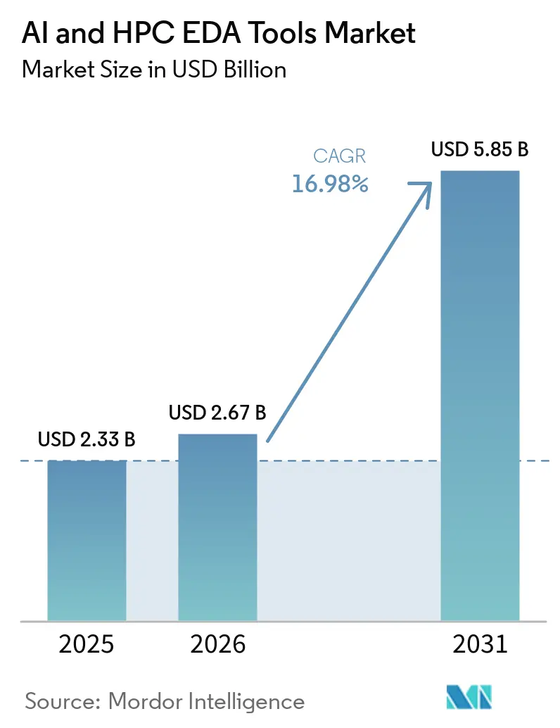
The AI and HPC EDA Tools Market size is expected to grow from USD 2.33 billion in 2025 to USD 2.67 billion in 2026 and is forecast to reach USD 5.85 billion by 2031 at 16.98% CAGR over 2026-2031. Demand accelerates as hyperscalers rush custom accelerators into production, advanced nodes below 7 nanometers multiply sign-off loops, and 3D-IC chiplets force tighter co-simulation of die-to-die links and thermal profiles. Verification workloads already dominate project timelines, yet packaging suites are the fastest-growing tool category because UCIe 3.0 calls for unified electrical-thermal-mechanical analysis. Cloud delivery is spreading from startups to large fabless teams that need 50,000-core emulation bursts but want to pay only when gates are switching. At the same time, U.S. export controls on sub-7-nanometer design flows have split global purchasing patterns and boosted regional champions in China.
Key Report Takeaways
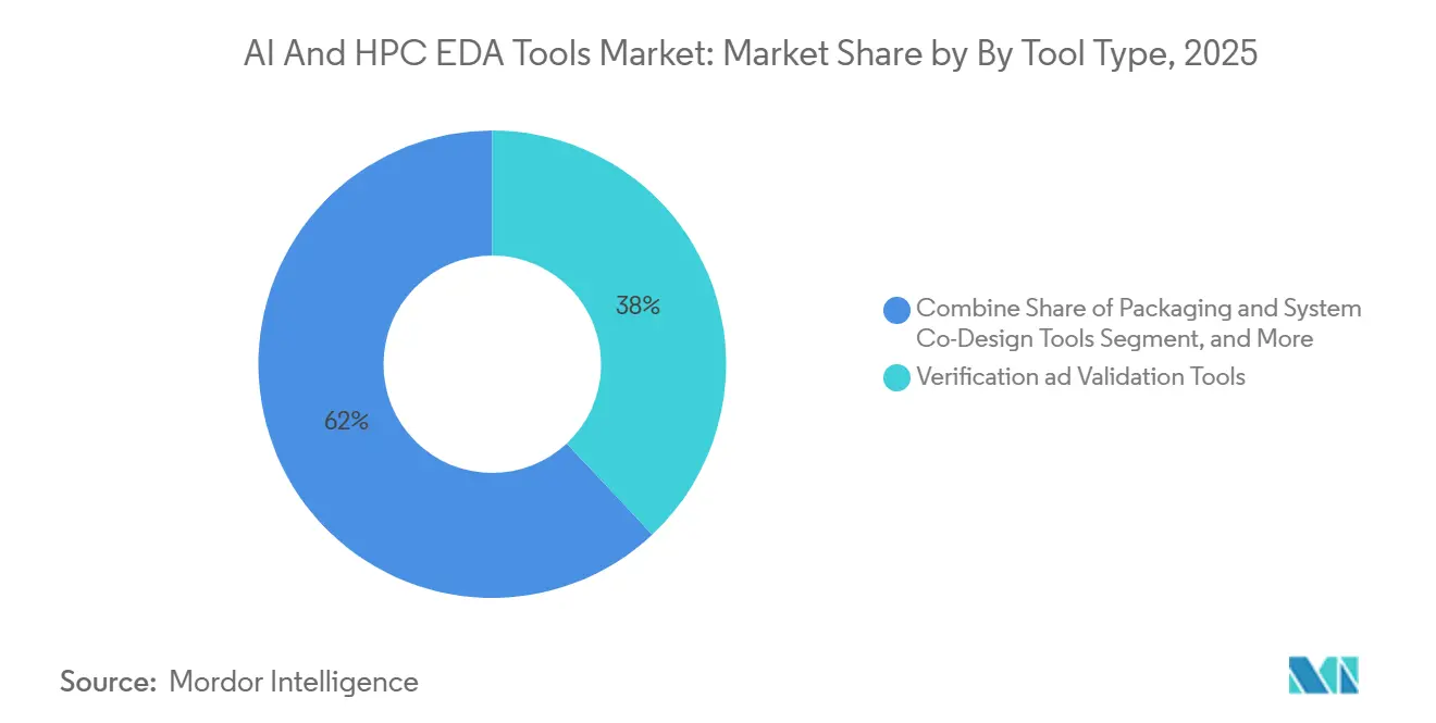
- By tool type, verification and validation led with 38.0% AI and HPC EDA tools market share in 2025; packaging and system co-design is advancing at an 18.6% CAGR to 2031.
- By deployment model, on-premise accounted for 76.0% of the AI and HPC EDA tools market in 2025, while cloud-based usage is projected to expand at a 20.7% CAGR through 2031.
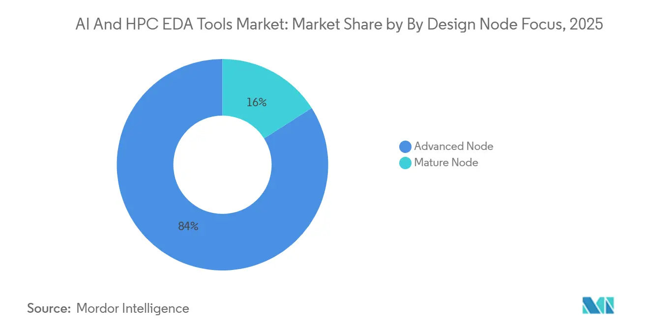
- By design node focus, advanced nodes at 7 nanometers and below captured 84.0% of the AI and HPC EDA tools market in 2025 sales and are growing at 17.6% annually.
- By end-user type, fabless semiconductor companies held 57.0% share of the AI and HPC EDA tools market size in 2025, whereas hyperscalers record the highest projected growth at 19.3% through 2031.
- By geography, North America led with 49.0% revenue of the AI and HPC EDA tools market in 2025, and Asia-Pacific is forecast to rise at a 17.1% CAGR to 2031.
Note: Market size and forecast figures in this report are generated using Mordor Intelligence’s proprietary estimation framework, updated with the latest available data and insights as of January 2026.
Market Trends and Insights
Drivers Impact Analysis of AI and HPC EDA Tools Market*
| Driver | (~) % Impact on CAGR Forecast | Geographic Relevance | Impact Timeline |
|---|---|---|---|
| Rapid Adoption of AI Accelerators in Data Centers | +4.20% | Global, concentrated in North America and Asia-Pacific hyperscaler hubs | Short term (≤ 2 years) |
| Rising Design Complexity at ≤7 nm Nodes | +3.80% | Taiwan, South Korea, United States | Medium term (2–4 years) |
| Shorter Tape-Out Cycles Demanding Advanced Verification | +3.10% | North America and Asia-Pacific fabless ecosystems | Short term (≤ 2 years) |
| Growing Cloud-Based EDA Consumption Models | +2.90% | North America and Europe | Medium term (2–4 years) |
| Co-Optimization Needs for 3D-IC Heterogeneous Integration | +2.20% | Asia-Pacific packaging hubs, North America design centers | Long term (≥ 4 years) |
| Open-Source Hardware Movement Expanding Verification Demand | +1.40% | North America and Europe | Long term (≥ 4 years) |
| Source: Mordor Intelligence | |||
Rapid Adoption Of AI Accelerators In Data Centers
Hyperscalers taped out more than 150 bespoke AI chips between 2024 and 2026, each featuring tensor cores, multi-terabit memory fabrics, and optical IO that stress verification flows. AWS Trainium 2 integrates 192 billion transistors on 5 nm and quadruples training throughput, forcing formal engines to validate 512 GB/s DRAM pipelines.[1]A. Peterson, “AWS Trainium 2 Architecture,” AboutAmazon, aboutamazon.com Google’s TPU v6e links 256 dies through optical circuit switches, so system-level emulation must model congestion and thermal throttling at rack scale. Meta’s MTIA v2 shifted to INT8-FP8 mixed precision, adding undocumented numeric corner cases that ballooned test-bench code by 40%. Startups such as Cerebras and Groq bypass standard place-and-route, yet still consume Synopsys Fusion Compiler for timing closure, further expanding the AI and HPC EDA tools market.
Rising Design Complexity At ≤7 nm Nodes
TSMC’s N2P gate-all-around process lifts design-rule checks by 60% over N3E, while Samsung’s SF2 node introduces multi-bridge channel FETs that require new vertical current models. Sign-off teams now spend up to 40% of project time on electromigration and IR-drop closure.[2]T.M. Nguyen, “Fiscal Year 2025 Financial Results,” Synopsys Investor Relations, investor.synopsys.com Siemens answered with Calibre Vision AI, cutting layout debug in half at three pilot customers.[3]R. Gupta, “Calibre Vision AI Cuts Debug Time,” press.siemens.com Intel’s 18A roadmap has already triggered pre-certification of EDA suites to secure early tape-outs, adding momentum across United States foundry sites INTEL.COM.
Shorter Tape-Out Cycles Demanding Advanced Verification
Average schedules tightened to 18-24 months by 2025. SiMa.ai hit a 14-month cadence using Cadence Palladium Z2 emulation combined with Xcelium parallel simulation. Cadence added Gemini-powered natural-language assertion generation in 2026, trimming verification planning by up to 30%. Ansys 2026 R1 merges electromagnetic and power analysis for single-pass sign-off of 3D-IC stacks. Regulatory carve-outs keep emulation hardware exportable, sustaining global revenue despite node controls.
Growing Cloud-Based EDA Consumption Models
Startups dodged USD 200,000-plus perpetual seats by shifting to pay-per-use clouds in 2025. Samsung SAFE Cloud now hosts certified 2 nm kits that users can burst to 10,000 cores.[4]D. Allen, “SAFE Cloud Design Platform Launch,” news.samsung.com Intel Foundry Services connects Synopsys.ai and Cadence ChipStack on Google Cloud, lowering 18A onboarding from weeks to hours INTEL.COM. Synopsys’ cloud revenue climbed 35% YoY, and Cadence said 40% of new deals include cloud, up from 25% two years earlier INVESTOR.SYNOPSYS.COM. Security concerns remain, so vendors now bundle confidential computing and homomorphic encryption that add 10-15% runtime overhead SEMI.ORG.
Restraints Impact Analysis of AI and HPC EDA Tools Market*
| Restraint | (~) % Impact on CAGR Forecast | Geographic Relevance | Impact Timeline |
|---|---|---|---|
| Escalating License Costs for Full Flow Toolchains | -1.80% | Global, acute for startups in North America and Asia-Pacific | Short term (≤ 2 years) |
| Talent Shortage in Advanced Node Physical Design | -1.50% | United States, Taiwan, India | Medium term (2–4 years) |
| Export Control Risks on EDA for Advanced Nodes | -1.20% | China and Russia, spillover to multinational vendors | Long term (≥ 4 years) |
| Verification Bottlenecks in Novel AI-Specific Data Types | -0.90% | Global, AI accelerator teams | Medium term (2–4 years) |
| Source: Mordor Intelligence | |||
Escalating License Costs For Full Flow Toolchains
At 2 nm, annual subscriptions surpass the USD 1 million mark due to foundries certifying only a limited set of tools. This restriction has allowed Synopsys and Cadence to secure a combined market share of 62%, solidifying their dominance. Siemens Caliber, on the other hand, employs a per-core pricing model, which drives the costs of large verification farms beyond USD 2 million annually. Furthermore, Arm's CPU and PHY royalties add to the financial strain, creating significant cost pressures for companies. In response, startups are increasingly turning to the open-source OpenROAD platform for initial design passes to manage expenses. However, this approach comes with a trade-off, as it can extend project schedules by up to 15%.
Talent Shortage In Advanced Node Physical Design
The United States needs 1 million additional semiconductor workers by 2030, yet engineering enrollments grow only 3% annually. This workforce shortage is evident in cities like Phoenix and Austin, where thousands of EDA positions remained unfilled in 2025, with senior salaries exceeding USD 180,000, according to GPEC.ORG. To address this gap, Siemens’ Fuse EDA AI Agent now automates 40% of constraint files, improving efficiency. However, the industry faces challenges such as high attrition rates in India, which reached 22% as engineers switched jobs for 30-40% salary increases. These trends highlight the growing demand for skilled talent and the need for innovative solutions to bridge the workforce gap.
*Our forecasts treat driver/restraint impacts as directional, not additive. The impact forecasts reflect baseline growth, mix effects, and variable interactions.
AI and HPC EDA Tools Market Segment Analysis
Packaging and system co-design tools command the highest forecast growth at 18.6% as chiplet adoption rises. Siemens Innovator3D IC integrates die-to-die protocol checks, thermal gradients, and power delivery, trimming assembly cycles by 50% at ASE Technology. Verification still led 2025 revenue with 38.0% because RTL simulation and formal proof remain unavoidable, keeping Cadence Xcelium and Synopsys VCS entrenched. Front-end design benefits from open-source SystemVerilog linters introduced by CHIPS Alliance, while back-end place-and-route at mature nodes faces price pressure from OpenROAD. Sign-off suites such as Caliber stay indispensable for foundry approval, anchoring predictable maintenance revenue.
Second-order effects are emerging. UCIe 3.0’s 64 GT/s bandwidth forces electro-thermal co-analysis inside the same run, turning multiphysics into a purchasing criterion. Small vendors that specialize in photonics or power integrity now plug their engines into mainstream flows through open APIs. Collectively, these dynamics cement the AI and HPC EDA tools market as a duopoly plus niche specialists.



By Deployment Model:
Consumption Pricing Spurs Cloud UptakeCloud-based usage is growing at an annual rate of 20.7%, outpacing the overall AI and HPC EDA tools market. This growth is driven by the pay-as-you-go model, which aligns well with the funding milestones of venture-backed startups. Cadence reported a 42% increase in ChipStack cloud revenue in 2026, while Synopsys gained 120 new cloud customers in 2025, with 80% of these being startups. Despite this growth, on-premise solutions still account for 76.0% of the market, primarily due to IDMs relying on sunk license costs and stringent IP security requirements. However, advancements such as safe-harbor enclaves and ISO 27001 audits have alleviated security concerns, enabling hyperscalers to deliver 50,000-core emulation bursts without requiring capital expenditure.
Cloud platforms are now capable of metering compute and storage resources together, transforming one-time software revenue into recurring service streams. This shift allows vendors to offer additional services, such as AI-assisted debugging, design-for-test, and power-analysis microservices, thereby increasing their share of customer spending. Furthermore, foundries are integrating certified workflows into their own portals, significantly reducing the time-to-first-tape-out from months to days. This integration not only enhances efficiency but also strengthens the appeal of cloud-based solutions in the market.
By Design Node Focus:
Advanced Nodes Sustain Premium PricingAdvanced nodes ≤7 nm accounted for 84.0% revenue in 2025 and will expand at 17.6% a year as N2P, SF2, and 18A processes hit volume. Each node forces customers to buy fresh sign-off decks and recalibrated extraction models, upping average selling prices. Mature nodes above 7 nm cater to automotive and industrial customers that care more about reliability than density; here, open-source flows reach 85-90% quality of result but still revert to commercial tools for ISO 26262 or TSMC green-flag. Export restrictions now compel Synopsys and Cadence to maintain dual branches, with sub-7 nm modules barred from unlicensed export, accelerating China’s investment in Empyrean Technology.
Advanced-node premiums have created opportunities for GPU-accelerated timing and power engines, co-developed by NVIDIA and Synopsys, which promise significant reductions in runtime, often in double digits. These advancements are particularly critical as backside power delivery and gate-all-around devices introduce new complexities. Physical verification now requires simultaneous modeling of vertical current and mechanical stress, adding to the challenges faced by the industry. To address these demands, customers are increasingly turning to integrated multiphysics suites, which offer comprehensive solutions. These suites help streamline processes and ensure accuracy in handling the intricate requirements of advanced semiconductor technologies.
By End-User Type:
Hyperscalers Drive The Next Revenue WaveFabless firms still anchor 57.0% of 2025 spend, but hyperscalers such as AWS, Google, Microsoft, and Meta grow the fastest at 19.3% as they insource silicon to trim data-center cost of ownership. AWS disclosed USD 1 billion yearly savings from Graviton and Trainium, directly recycling funds into more EDA licenses. These companies negotiate bespoke feature roadmaps: NVIDIA invested USD 2 billion in Synopsys for GPU-accelerated algorithms and agentic AI assistants. By contrast, IDMs secure multi-year enterprise agreements that keep vendor revenue steady but limit upside.
Vertical integration by cloud providers is causing a fragmentation of demand in the market. Hyperscalers frequently collaborate with foundries to co-design chips, bypassing traditional turnkey IP solutions. They often require open interfaces into place-and-route engines to enable proprietary optimizations, which adds complexity to the process. To address these challenges, EDA suppliers are establishing dedicated customer-success pods. These pods involve embedding engineers on-site with clients for extended periods, often lasting several months, to provide tailored support and ensure seamless integration. This approach helps EDA suppliers meet the unique demands of hyperscalers while maintaining competitive service levels.
Geography Analysis
North America AI and HPC EDA Tools Market
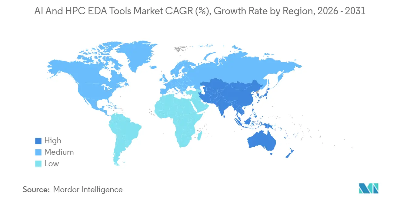
North America led with 49.0% of 2025 revenue owing to Silicon Valley fabless giants, Seattle-based hyperscalers, and massive CHIPS Act incentives. TSMC’s Phoenix N3 fab alone spawned a 200-person design-enablement team that pre-certifies flows and added USD 50 million in local tool sales. Intel Foundry Services is courting Microsoft and Amazon for early 18A tape-outs via a cloud-first EDA bundle, further deepening regional spend. U.S. export controls, however, removed roughly USD 1.5 billion in combined Synopsys and Cadence sales to China, redirecting vendor attention to domestic and allied customers.
APAC AI and HPC EDA Tools Market
Asia-Pacific is the fastest-growing territory at a 17.1% CAGR as TSMC and Samsung roll out gate-all-around nodes, China accelerates self-sufficiency, India scales design centers, and Japan’s Rapidus pursues 2 nm logic. Chinese customers, blocked from sub-7 nm Western tools, now align with Empyrean for 14 nm and 28 nm projects, producing double-digit domestic growth. India’s attrition-plagued talent pool still attracts multinationals that tap lower-cost verification teams. Japan’s government-backed Rapidus forces Synopsys and Cadence to station process-node experts in Tokyo to keep pace with IBM-licensed technology, while South Korea’s diversification beyond memory enlarges the regional addressable market.
EMEA and South America AI and HPC EDA Tools Market
Europe, South America, Middle East and Africa share the remaining slice. European funding centers on automotive and industrial ICs at mature nodes, limiting uptake of bleeding-edge sign-off suites. Israeli design houses contribute niche SerDes and AI-inference verification demand, yet volumes remain modest. Saudi Arabia announced a USD 100 billion chip program in 2025, but commercial flows are years away, placing the region at the earliest stage of the adoption curve.

Competitive Landscape
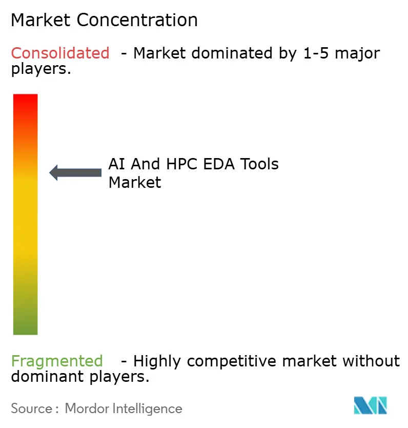
Synopsys and Cadence held a combined 62% share in 2025, confirming a high-concentration structure that discourages price wars. Synopsys closed its USD 35 billion Ansys takeover in 2025, bundling thermal, electromagnetic, and mechanical solvers into a single pass for 3D-IC sign-off. Keysight then scooped up divested photonics and low-power assets to enlarge its PathWave platform. NVIDIA’s USD 2 billion strategic stake in Synopsys will deliver GPU-accelerated route-and-place and digital-twin toolkits, underscoring the convergence of compute infrastructure and design software.
Niche challengers focus on gaps the duopoly cannot wholly fill. CHIPS Alliance’s open-source SV Tools narrows entry barriers for RISC-V startups, while Siemens Fuse AI Agent automates constraint scripts to stretch limited engineering headcount. Empyrean Technology surges inside China as localization mandates shift spending toward domestic solutions. Regulatory friction also shapes the field: U.S. export controls forced Synopsys to curtail Chinese deals, while the FTC demanded tool divestitures to preserve competition, giving Keysight an instant foothold in power-artist workflows.
In photonics, silicon interposer growth pushes vendors like Ansys Lumerical and Synopsys RSoft, now under Keysight, into mainstream chiplet flows. Power integrity and thermal co-analysis emerge as battlegrounds where multiphysics performance wins POs. Meanwhile, open-source initiatives accelerate: OpenROAD produced a 28 nm RISC-V tape-out, proving 90% parity on mature nodes and hinting at longer-term commoditization of foundational place-and-route capabilities.
AI and HPC EDA Tools Industry Leaders
Synopsys, Inc.
Cadence Design Systems, Inc.
Siemens Digital Industries Software
Ansys, Inc.
Keysight Technologies, Inc.
- *Disclaimer: Major Players sorted in no particular order
AI and HPC EDA Tools Market Companies Covered in this Report
- Synopsys, Inc.
- Cadence Design Systems, Inc.
- Siemens Digital Industries Software
- Ansys, Inc.
- Keysight Technologies, Inc.
- Empyrean Technology Co., Ltd.
- Silvaco, Inc.
- Aldec, Inc.
- Blue Pearl Software, Inc.
- Real Intent, Inc.
- Arteris, Inc.
- Mirabilis Design, Inc.
- Pulsic Limited
- Sigasi NV
- Xilinx, Inc. (AMD)
- Arm Limited
- OpenFive, Inc.
- Easy-Logic Technology Co., Ltd.
- Concept Engineering GmbH
- Flex Logix Technologies, Inc.

Recent Industry Developments in AI and HPC EDA Tools Market
- April 2026: Siemens Digital Industries Software and TSMC partnered to embed Fuse EDA AI Agent inside N2P and A16 design kits, promising 20-30% verification-cycle reductions.
- April 2026: Cadence integrated Google’s Gemini LLM into Virtuoso and Genus, enabling plain-language test-bench creation that cut planning effort by 25%.
- April 2026: Sarcina Technology introduced UCIe-A and UCIe-S IP blocks certified at 64 GT/s for chiplet assemblies in AI accelerators.
- March 2026: CHIPS Alliance launched SV Tools Project, providing open-source Verible linters and Synlig synthesis for RISC-V cores.


Global AI and HPC EDA Tools Market Report Scope
The AI and HPC EDA Tools Market Report is Segmented by Tool Type (Front-End Design Tools, Verification and Validation Tools, Physical Design (Back-End) Tools, Signoff and Analysis Tools, Packaging and System Co-Design Tools), Deployment Model (On-Premise, Cloud-Based), Design Node Focus (Advanced Node ≤7nm, Mature Node >7nm), End-User Type (Large Fabless and IDMs, AI Chip Startups), End-User (Fabless Semiconductor Companies, Integrated Device Manufacturers, Hyperscalers), and Geography (North America, Europe, Asia-Pacific, Rest of the World). The Market Forecasts are Provided in Terms of Value (USD).
| Front-End Design Tools |
| Verification and Validation Tools |
| Physical Design (Back-End) Tools |
| Signoff and Analysis Tools |
| Packaging and System Co-Design Tools |
| On-Premise |
| Cloud-Based |
| Advanced Node (?7nm) |
| Mature Node (>7nm) |
| By End-User Type |
| Large Fabless & IDMs |
| AI Chip Startups |
| Fabless Semiconductor Companies |
| Integrated Device Manufacturers (IDMs) |
| Hyperscalers |
| North America | United States |
| Canada | |
| Mexico | |
| Europe | Germany |
| United Kingdom | |
| Rest of Europe | |
| Asia-Pacific | China |
| Japan | |
| South Korea | |
| India | |
| Rest of Asia-Pacific | |
| Rest of the World |
| By Tool Type | Front-End Design Tools | |
| Verification and Validation Tools | ||
| Physical Design (Back-End) Tools | ||
| Signoff and Analysis Tools | ||
| Packaging and System Co-Design Tools | ||
| By Deployment Model | On-Premise | |
| Cloud-Based | ||
| By Design Node Focus | Advanced Node (?7nm) | |
| Mature Node (>7nm) | ||
| By End-User Type | ||
| Large Fabless & IDMs | ||
| AI Chip Startups | ||
| By End-User | Fabless Semiconductor Companies | |
| Integrated Device Manufacturers (IDMs) | ||
| Hyperscalers | ||
| By Geography | North America | United States |
| Canada | ||
| Mexico | ||
| Europe | Germany | |
| United Kingdom | ||
| Rest of Europe | ||
| Asia-Pacific | China | |
| Japan | ||
| South Korea | ||
| India | ||
| Rest of Asia-Pacific | ||
| Rest of the World | ||


Key Questions Answered in the Report
What is the current size of the AI and HPC EDA tools market?
The AI and HPC EDA tools market size stood at USD 2.67 billion in 2026 and is projected to reach USD 5.85 billion by 2031.
Which tool category is growing the fastest?
Packaging and system co-design tools are forecast to grow at an 18.6% CAGR because 3D-IC and chiplet architectures require integrated electro-thermal-mechanical analysis.
Why are hyperscalers investing heavily in EDA tools?
AWS, Google, Microsoft, and Meta build custom silicon to trim data-center cost of ownership, and their vertically integrated design cycles demand expansive verification and emulation capacity.
How are export controls affecting the industry?
U.S. rules that restrict sub-7 nm EDA sales to China eliminated around USD 1 billion in vendor revenue and accelerated domestic Chinese investment in indigenous alternatives such as Empyrean Technology.
What is driving the migration of EDA workloads to the cloud?
Pay-per-use pricing, elastic compute for massive emulation jobs, and pre-certified foundry design kits reduce capex and shrink time-to-tape-out for startups and mid-tier fabless firms.
Where is the most severe talent shortage?
Advanced-node physical design faces acute shortages in the United States, Taiwan, and India, prompting vendors to embed AI agents that automate constraint generation and debug triage.
Page last updated on: