AI And HPC Semiconductor Silicon Wafer Market Size and Share
Market Overview
| Study Period | 2020 - 2031 |
|---|---|
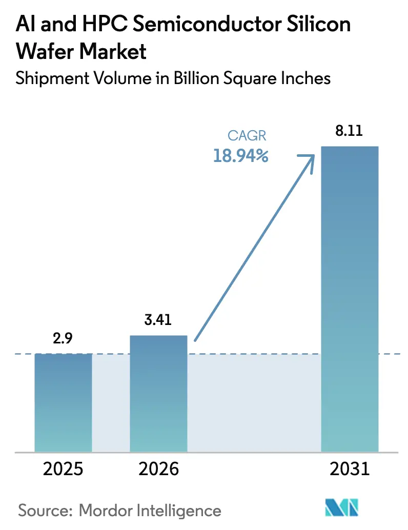
| Market Volume (2026) | 3.41 Billion Square Inches |
| Market Volume (2031) | 8.11 Billion Square Inches |
| Growth Rate (2026 - 2031) | 18.94% CAGR |
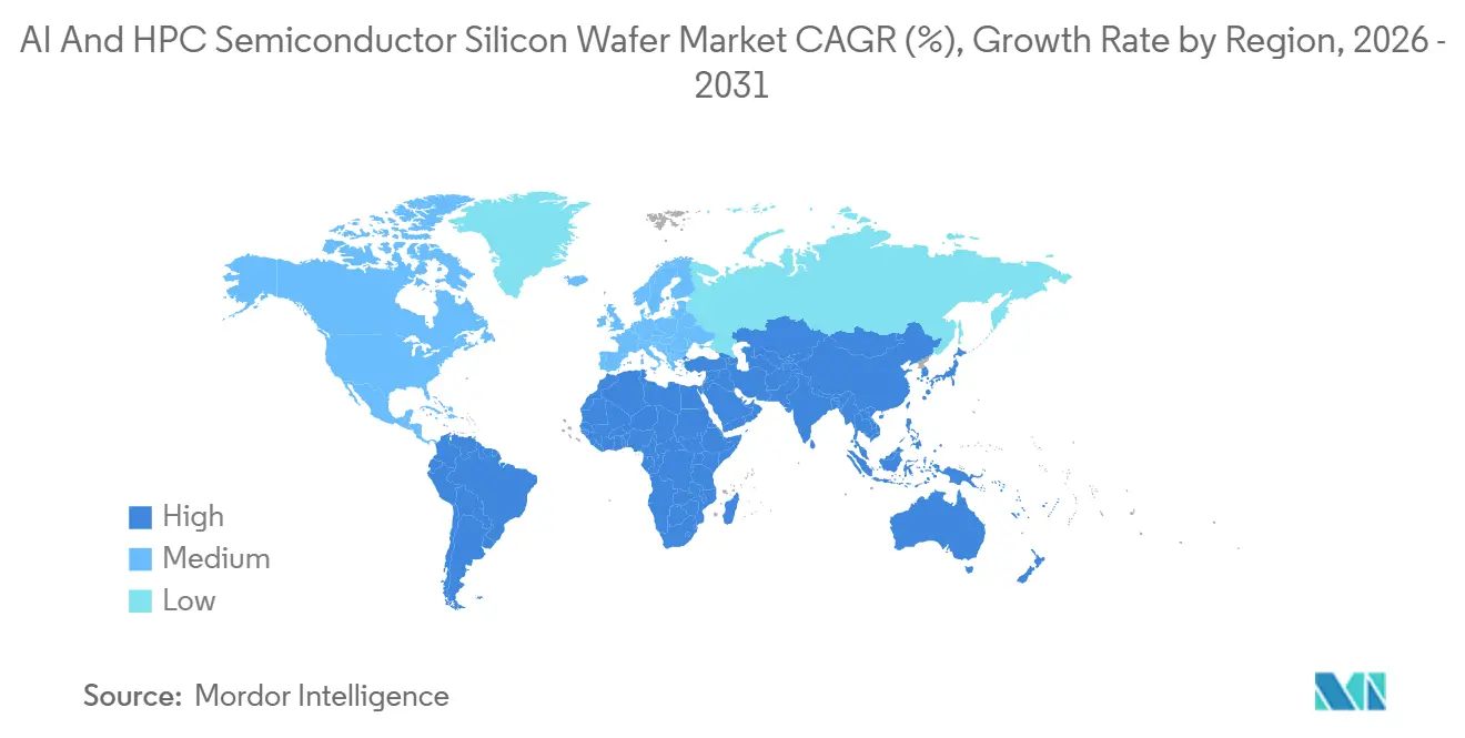
| Fastest Growing Market | Asia Pacific |
| Largest Market | Asia Pacific |
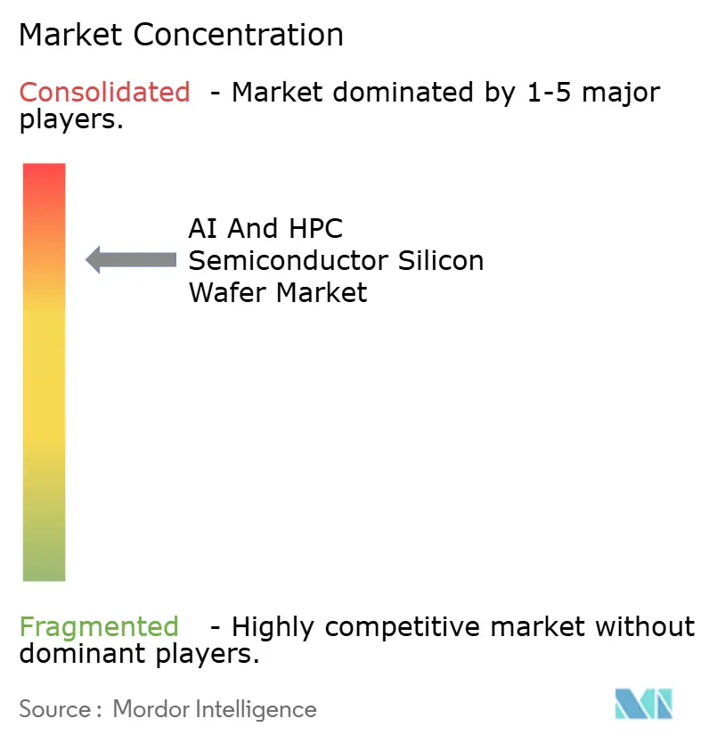
| Market Concentration | High |
Major Players *Disclaimer: Major Players sorted in no particular order Image © Mordor Intelligence. Reuse requires attribution under CC BY 4.0. | |
AI And HPC Semiconductor Silicon Wafer Market Analysis by Mordor Intelligence
The AI and HPC semiconductor silicon wafer market size is projected to expand from 2.9 billion square inches in 2025 and 3.41 billion square inches in 2026 to 8.11 billion square inches by 2031, registering a CAGR of 18.94% between 2026 to 2031. Capacity secured for sub-3-nanometer logic, multi-year offtake deals tied to sovereign subsidy programs, and the migration toward inference-optimized accelerators collectively reinforce demand momentum. Taiwan, South Korea, the United States, and China are expanding 300 millimeter lines faster than crystal-pulling equipment can be delivered, tightening spot availability and lifting contract prices. Asian foundries no longer crowd out Western peers, because parallel subsidy corridors in Washington, Brussels, and Beijing have seeded geographically balanced investments. Taken together, these factors position wafer suppliers with flatness and defect-density leadership to capture structurally higher margins through the decade.
Key Report Takeaways
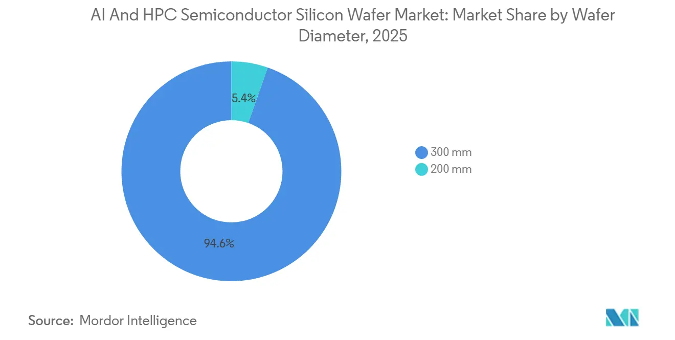
- By wafer diameter, the 300 mm category held 94.64% of the market share in 2025, and is forecast to advance at a 19.68% CAGR through 2031.
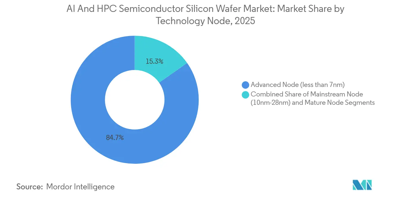
- By technology node, the advanced node (below 7nm) captured 84.73% of the market share in 2025, and is projected to grow at a 19.76% CAGR through 2031.
- By geography, Asia-Pacific commanded 74.62% of the market share in 2025, and is expected to expand at a 19.82% CAGR over 2026-2031.
Note: Market size and forecast figures in this report are generated using Mordor Intelligence’s proprietary estimation framework, updated with the latest available data and insights as of January 2026.
Global AI And HPC Semiconductor Silicon Wafer Market Trends and Insights
Drivers Impact Analysis*
| Driver | (~) % Impact on CAGR Forecast | Geographic Relevance | Impact Timeline |
|---|---|---|---|
| Surging Demand for 300 Mm Wafers in AI Accelerators | +4.5% | Global, with concentration in Taiwan, South Korea, United States | Short term (≤ 2 years) |
| Rapid Foundry Expansions Below 7 Nm in Taiwan and the United States | +4.2% | Taiwan, United States, with spillover to Japan | Medium term (2-4 years) |
| Growing Capital Support for Domestic Wafer Fabs in China | +3.1% | China, with indirect impact on Asia-Pacific supply chains | Medium term (2-4 years) |
| Aggressive Node Shrinks for Advanced HPC GPUs | +2.8% | Global, led by North America design hubs and Taiwan manufacturing | Short term (≤ 2 years) |
| Adoption of Backside-Power Delivery and Wafer-Level Bonding | +2.3% | Taiwan, South Korea, United States advanced packaging clusters | Medium term (2-4 years) |
| Sustainability Mandates Driving Prime Wafer Recycling | +1.2% | Europe, Japan, with emerging adoption in North America | Long term (≥ 4 years) |
| Source: Mordor Intelligence | |||
Surging Demand for 300mm Wafers in AI Accelerators
Hyperscale operators purchased 1.2 million accelerator cards in 2025, with each unit consuming up to 1,200 mm² of silicon on 300 millimeter substrates, a footprint 40% larger than general-purpose CPUs. Chip-on-wafer-on-substrate packaging doubles wafer usage per GPU because multiple reticle-limited dies share a single interposer. Transition plans by Microsoft and Meta to launch proprietary 3 nanometer inference processors in 2026 further lift demand pressure.[1]Michael Acton, “Microsoft and Meta Plan Proprietary AI Chips on 3nm Nodes,” Financial Times, ft.com The economic obsolescence of 200 millimeter substrates for leading-edge logic concentrates volume on 300 millimeter lines that can hold total-thickness variation below 0.15 µm. Fewer than five global suppliers currently meet that tolerance, which preserves oligopolistic pricing power through the forecast horizon.
Rapid Foundry Expansions Below 7nm in Taiwan and the United States
TSMC committed USD 65 billion to Arizona plants that began shipping 4 nanometer engineering wafers in December 2025. Samsung’s Pyeongtaek campus added a fifth cleanroom for 2 nanometer gate-all-around devices slated for mid-2026 volume.[2]Joon-hee Lee, “Samsung Foundry Expands Pyeongtaek Campus,” Samsung Electronics, news.samsung.com Intel’s Ohio project will reach 60,000 wafer starts per month on 18A in 2027. These three programs alone add 300,000 starts monthly by 2028, though equipment bottlenecks push full output 12-18 months to the right. Taiwan’s share of sub-7 nanometer capacity therefore declines from 92% in 2023 to roughly 78% in 2027, diffusing geopolitical risk but introducing jurisdictional export-control frictions that complicate cross-border logistics.
Growing Capital Support for Domestic Wafer Fabs in China
Phase III of China’s Big Fund allocated RMB 150 billion (USD 21 billion) in 2024, with 30% ring-fenced for upstream materials.[3]Yoko Kubota, “China State Council Allocates RMB 150 Billion to Semiconductor Fund,” South China Morning Post, scmp.com Shanghai Simgui’s Lingang project will ship 1.8 million 300 millimeter substrates annually by 2027, servicing 28 nanometer and 14 nanometer nodes. Domestic procurement by SMIC doubled to 32% in 2025. Despite volume gains, Chinese defect rates average 0.08 cm⁻² versus 0.03 cm⁻² for Japanese grades, limiting penetration below 10 nanometers. Incumbent suppliers face discount pressure to defend share but retain an edge in advanced-node qualifications.
Aggressive Node Shrinks for Advanced HPC GPUs
NVIDIA’s Blackwell B200 packs 208 billion transistors on TSMC N3E, a 60% density uplift over Hopper. AMD’s MI350, scheduled for 2027, will exploit backside power delivery at 3 nanometers. Intel’s Falcon Shores aims for 18A in 2026 and 14A in 2028, each step demanding wafers flatter than 0.12 µm. Suppliers must retrofit crystal-pullers with diameter-control algorithms and add epitaxial capacity, pushing capex beyond USD 500 million per line. Shrink cadence has tightened from 24 months to 18 months, compressing depreciation windows and favoring producers with deep balance sheets.
Restraints Impact Analysis*
| Restraint | (~) % Impact on CAGR Forecast | Geographic Relevance | Impact Timeline |
|---|---|---|---|
| Supply Chain Fragility for Ultrapure Polysilicon | -1.8% | Global, with acute exposure in North America and Europe | Short term (≤ 2 years) |
| Long Lead Times on Crystal-Pulling Equipment | -1.5% | Global, affecting all wafer producers | Medium term (2-4 years) |
| High Capex Intensity Limiting New Entrants | -1.2% | Emerging markets, China domestic suppliers | Long term (≥ 4 years) |
| Water and Power Scarcity Risks at Mega-Fabs | -0.9% | United States Southwest, Taiwan during drought cycles | Medium term (2-4 years) |
| Source: Mordor Intelligence | |||
Supply Chain Fragility for Ultrapure Polysilicon
Seven firms produced nearly all semiconductor-grade polysilicon in 2025, with Wacker, Hemlock, and Tokuyama covering 65%. Solar demand lifted spot prices from USD 28/kg to USD 41/kg during the year. U.S. forced-labor rules blocked Xinjiang origin, removing 40,000 t of capacity. Tokuyama’s Sarawak expansion adds 10,000 t in mid-2026 but needs 18 months of qualification. Smaller wafer houses without long contracts therefore face feedstock rationing, which could shave nearly 2 percentage points off the forecast CAGR if unmitigated.
Long Lead Times on Crystal-Pulling Equipment
Czochralski furnaces capable of sub-0.1 µm diameter variation averaged 20-month delivery times in 2025.[4]SEMI Staff, “Equipment Lead Times Extend to 20 Months,” SEMI, semi.org Ferrotec’s backlog equals 2.3 years of revenue, delaying Siltronic and SK Siltron additions. Shortages of high-purity graphite crucibles and seed rods, both under export control, compound delays. Some producers refurbish 200 millimeter lines, but that approach diverts engineering talent needed for 300 millimeter ramps. Industry capacity growth thus remains capped near 12% annually until at least 2027.
*Our forecasts treat driver/restraint impacts as directional, not additive. The impact forecasts reflect baseline growth, mix effects, and variable interactions.
Segment Analysis
By Wafer Diameter: 300 Millimeter Lines Secure Cost Leadership
The 300 mm segment of the AI and HPC semiconductor silicon wafer market accounted for 94.64% of the market share in 2025, reflecting its superior die-yield economics. Every 300 millimeter disk offers roughly 2.4× usable area versus a 200 millimeter substrate, reducing manufacturing expense per transistor by 30-40%. Foundry packaging flows, such as TSMC CoWoS, only accept 300 millimeter interposers, which lock hyperscale buyers into this diameter. Intel’s upcoming backside power architecture tightens total-thickness budgets to 0.12 µm, a figure unreachable on legacy 200 millimeter tools. Consequently, suppliers that master ultra-flat 300 millimeter crystals hold preferred-vendor status at all advanced logic fabs.
Growth momentum is unlikely to abate, as hyperscalers plan to produce custom inference chips on 3-nanometer nodes from 2026 onward. The segment’s 19.68% CAGR, therefore, exceeds the broader AI and HPC semiconductor silicon wafer market size trajectory as measured in square inches. Conversely, demand for 200 millimeter wafers is growing steadily, driven by FD-SOI and silicon-carbide applications where die sizes remain small. Equipment vendors have begun to sunset 150 millimeter service, forcing older fabs either to migrate or exit, a trend that accelerates consolidation. Recent M&A, such as GlobalWafers acquiring Siltronic’s Singapore asset, places more than one-quarter of non-Chinese 300 millimeter capacity under one owner, reshaping bargaining dynamics with foundry customers.


By Technology Node: Sub-7 Nanometer Premiums Intensify Margin Pool
Advanced geometries below 7 nanometers accounted for 84.73% of the market share in 2025 and will register a 19.76% CAGR through 2031. Each wafer in this node class ships with defect density below 0.03 cm⁻², metal contamination under 1 × 10¹⁰ atoms/cm³, and often includes epitaxial layers that add USD 150–200 to cost. Those specifications justify a 40% price premium, which enlarges the profit concentration inside the AI and HPC semiconductor silicon wafer market share controlled by Shin-Etsu, Sumco, and GlobalWafers. Gate-all-around devices debuting at Samsung in 2026 and at TSMC in 2027 intensify flatness requirements, compelling smaller vendors either to invest or retreat.
Mainstream nodes spanning 10–28 nanometers grow a steadier 11.2% because automotive and industrial buyers prefer mature IP cores and longer qualification cycles. Contracts signed by NXP and Infineon lock wafer prices through 2027 but offer little upside for suppliers as inflation lifts utility bills. Mature nodes above 28 nanometers feel margin squeeze from expanding Chinese capacity, yet they remain indispensable for radiation-hardened military silicon. This bifurcation means the premium segment harvests outsized returns while legacy nodes deliver volume stability, allowing producers to balance risk across the entire AI and HPC semiconductor silicon wafer market portfolio.

Geography Analysis
Asia-Pacific retained 74.62% of the market share in 2025 and is forecast to advance at 19.82% through 2031. TSMC alone consumed 800,000 starts per month across Taiwan, while its new Kumamoto plant in Japan adds 55,000 starts in late 2026. Samsung’s Pyeongtaek campus reached 400,000 starts monthly after the P4 line came online in 2025. China lifted domestic wafer sourcing to 32% by 2025, substituting imports despite defect-density disparities, and poured RMB 150 billion into upstream materials. Japan attracted JPY 4 trillion (USD 27 billion) in subsidies that hedge against Taiwan concentration, raising regional competition for skilled labor.
North America, though smaller, expands rapidly under CHIPS Act incentives. Intel’s Arizona and Ohio sites will draw 120,000 starts monthly by 2028, while TSMC’s Phoenix module already ships 4 nanometer silicon. GlobalWafers broke ground on a USD 5 billion Sherman, Texas plant, aiming for 1.2 million wafers annually. Water scarcity surfaced as a binding constraint, with Arizona fabs consuming 4 million gallons daily, prompting regulators to mandate 90% reuse targets that only TSMC currently meets. Achieving sustainable water intensity is now a gating factor for future incentive disbursements.
Europe captured 8% of global square-inch output in 2025, specializing in automotive and power devices. Infineon’s Dresden fab and STMicroelectronics’ Crolles site pull wafers from Siltronic’s Freiberg plant to satisfy Chips Act local-content rules. Bosch added a 200 millimeter line in Reutlingen to ease vehicle-sensor shortages but remains reliant on imports for leading-edge logic. South America and the Middle East and Africa together account for less than 2% of volume and host no prime-wafer facilities, exposing local assemblers to shipping and tariff shocks when Asia-Pacific logistics tighten.

Competitive Landscape
The AI and HPC semiconductor silicon wafer market is concentrated with playes such as Shin-Etsu, Sumco, GlobalWafers supply and others. Their volume scale supports continuous capex for defect-density leadership, currently at 0.03 cm⁻² for Shirakawa and Imari plants. Foundries increasingly negotiate equity stakes to lock supply; TSMC’s 2025 polysilicon joint venture with Tokuyama typifies this vertical-integration push. Smaller vendors such as Wafer Works and Episil-Precision focus on specialty epitaxial and SOI niches where defect budgets are less stringent, but their aggregate share stays below 10%.
Technology differentiation hinges on flatness, crystal orientation, and metallic contamination. Shin-Etsu pioneered real-time diameter monitoring that cuts total-thickness variation below 0.09 µm, a threshold essential for 2 nanometer backside power rails. Sumco’s Imari expansion earmarks epitaxial wafers for 1.6 nanometer research programs, signaling a bid to defend premium ASPs. GlobalWafers’ acquisition of Siltronic’s Singapore asset vaults it to number two globally and gives it a manufacturing beachhead in Southeast Asia, lowering shipping lead times to Taiwan and Japan.
Sustainability adds a new competitive dimension. European automotive OEMs now require ISO 14064 certification for carbon neutrality, which Siltronic’s Freiberg site achieved in 2025. TSMC and Samsung demand water-recovery rates above 85% at supplier plants, forcing capex on recycling loops. Reclaimed prime wafers for test operations represent a small but growing niche where Soitec positions FD-SOI substrates that cut power by 30% versus bulk silicon. High entry costs, multi-year qualifications, and deep customer-supplier engineering ties make disruptive entry unlikely before alternate materials, such as silicon-germanium or gallium-oxide, reach commercial maturity.
AI And HPC Semiconductor Silicon Wafer Industry Leaders
Shin-Etsu Chemical Co., Ltd.
Sumco Corporation
GlobalWafers Co., Ltd.
Siltronic AG
SK Siltron Co., Ltd.
- *Disclaimer: Major Players sorted in no particular order

Recent Industry Developments
- February 2026: GlobalWafers completed the acquisition of Siltronic’s Singapore 300 millimeter plant for EUR 3.8 billion (USD 4.1 billion), triggering EU antitrust review.
- January 2026: TSMC announced a USD 12 billion Kumamoto expansion that will add 55,000 300 millimeter starts per month for 6 nanometer and 7 nanometer nodes.
- December 2025: Shin-Etsu inaugurated a Shirakawa 300 millimeter line with 600,000 annual capacity, focused on wafers for 2 nanometer logic.
- November 2025: Samsung Foundry signed a USD 6.4 billion wafer contract with Qualcomm covering 3 nanometer Snapdragon processors through 2027.


Global AI And HPC Semiconductor Silicon Wafer Market Report Scope
The AI and HPC Semiconductor Silicon Wafer Market focuses on the production and utilization of silicon wafers specifically designed for artificial intelligence (AI) and high-performance computing (HPC) applications. These wafers serve as the foundational material for semiconductor devices, enabling advanced processing capabilities required in AI and HPC systems.
The AI and HPC Semiconductor Silicon Wafer Market Report is segmented by Wafer Diameter (300mm and 200mm), Technology Node (Advanced Node, Mainstream Node, and Mature Node), and Geography (North America, Europe, Asia-Pacific, South America, and the Middle East and Africa). The Market Forecasts are Provided in Terms of Volume (Square Inches).
| 300 mm |
| 200 mm |
| Advanced Node (Below 7nm) |
| Mainstream Node (10nm-28nm) |
| Mature Node (Above 28nm) |
| North America | United States |
| Canada | |
| Mexico | |
| Europe | Germany |
| United Kingdom | |
| France | |
| Rest of Europe | |
| Asia-Pacific | China |
| Japan | |
| India | |
| South Korea | |
| Taiwan | |
| Rest of Asia-Pacific | |
| South America | |
| Middle East and Africa |
| By Wafer Diameter | 300 mm | |
| 200 mm | ||
| By Technology Node | Advanced Node (Below 7nm) | |
| Mainstream Node (10nm-28nm) | ||
| Mature Node (Above 28nm) | ||
| By Geography | North America | United States |
| Canada | ||
| Mexico | ||
| Europe | Germany | |
| United Kingdom | ||
| France | ||
| Rest of Europe | ||
| Asia-Pacific | China | |
| Japan | ||
| India | ||
| South Korea | ||
| Taiwan | ||
| Rest of Asia-Pacific | ||
| South America | ||
| Middle East and Africa | ||


Key Questions Answered in the Report
What is the forecasted market size of AI and HPC semiconductor silicon wafers by 2031?
The market is expected to reach 8.11 billion square inches by 2031, reflecting an 18.94% CAGR from 2026 to 2031.
Which wafer diameter is preferred for advanced accelerators?
The 300 millimeter diameter already accounts for 94.64% of the market share in 2025 and is projected to keep expanding at a 19.68% CAGR through 2031.
How fast are sub-7 nanometer nodes expanding?
Shipments tied to geometries below 7 nanometers are set to grow at a 19.76% CAGR, fueled by next-generation GPUs and custom inference chips.
Which region contributes the largest consumption of prime wafers?
Asia-Pacific provided 74.62% of the market share in 2025 and is projected to rise at a 19.82% CAGR, anchored by capacity additions in Taiwan, South Korea, China, and Japan.
What two bottlenecks could slow near-term capacity additions?
Limited availability of ultra-pure polysilicon and 20-month lead times for crystal-pulling equipment constrain how quickly new wafer output can come online.
Page last updated on:


