Through-Silicon Via (TSV) For GPU and AI Accelerators Market Size and Share
Market Overview
| Study Period | 2020 - 2031 |
|---|---|
| Market Size (2026) | USD 11.54 Billion |
| Market Size (2031) | USD 32.69 Billion |
| Growth Rate (2026 - 2031) | 23.15 % |
| Fastest Growing Market | North America |
| Largest Market | Asia-Pacific |
| Market Concentration | Medium |
Major Players *Disclaimer: Major Players sorted in no particular order Image © Mordor Intelligence. Reuse requires attribution under CC BY 4.0. | |
Through-Silicon Via (TSV) For GPU and AI Accelerators Market Analysis by Mordor Intelligence
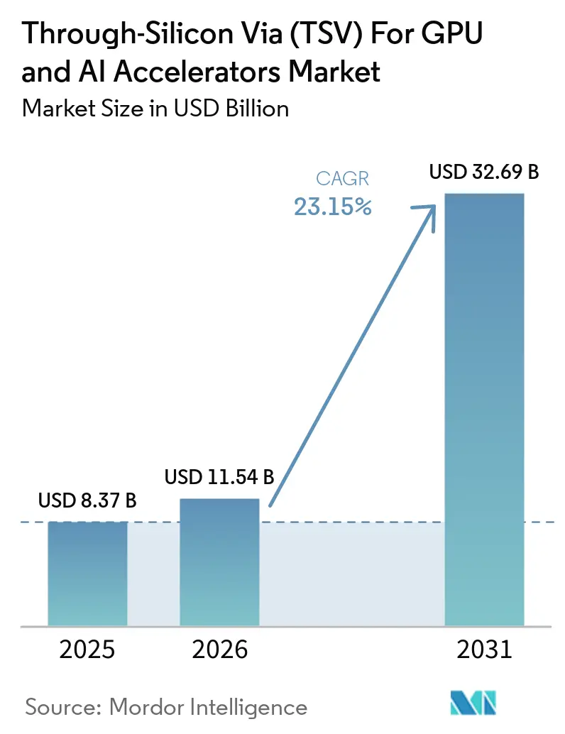
The Through-Silicon Via for GPU and AI accelerators marke size is projected to be USD 8.37 billion in 2025, USD 11.54 billion in 2026, and reach USD 32.69 billion by 2031, at a CAGR of 23.15% during the forecast period (2026-2031). Explosive adoption of high-bandwidth memory (HBM) in generative-AI GPUs, the pivot to chiplet-based graphics architectures, and multibillion-dollar investments in 2.5D and 3D packaging lines are reshaping value creation. Foundry-owned advanced-packaging platforms such as TSMC CoWoS and Samsung I-Cube increasingly determine time-to-market, shifting competitive advantage from transistor density to vertical-interconnect density. Governments are underwriting domestic capacity through subsidy schemes that compress equipment lead times and intensify competition for process engineers. Equipment leaders are benefiting from demand spikes in wafer-to-wafer bonding, TSV etch, and reveal tools, even as yield drag, thermal constraints, and geopolitical export controls temper short-term output growth. Against this backdrop, the Through-Silicon Via (TSV) market for GPU and AI accelerators is gaining strategic relevance across the semiconductor ecosystem.
Key Report Takeaways
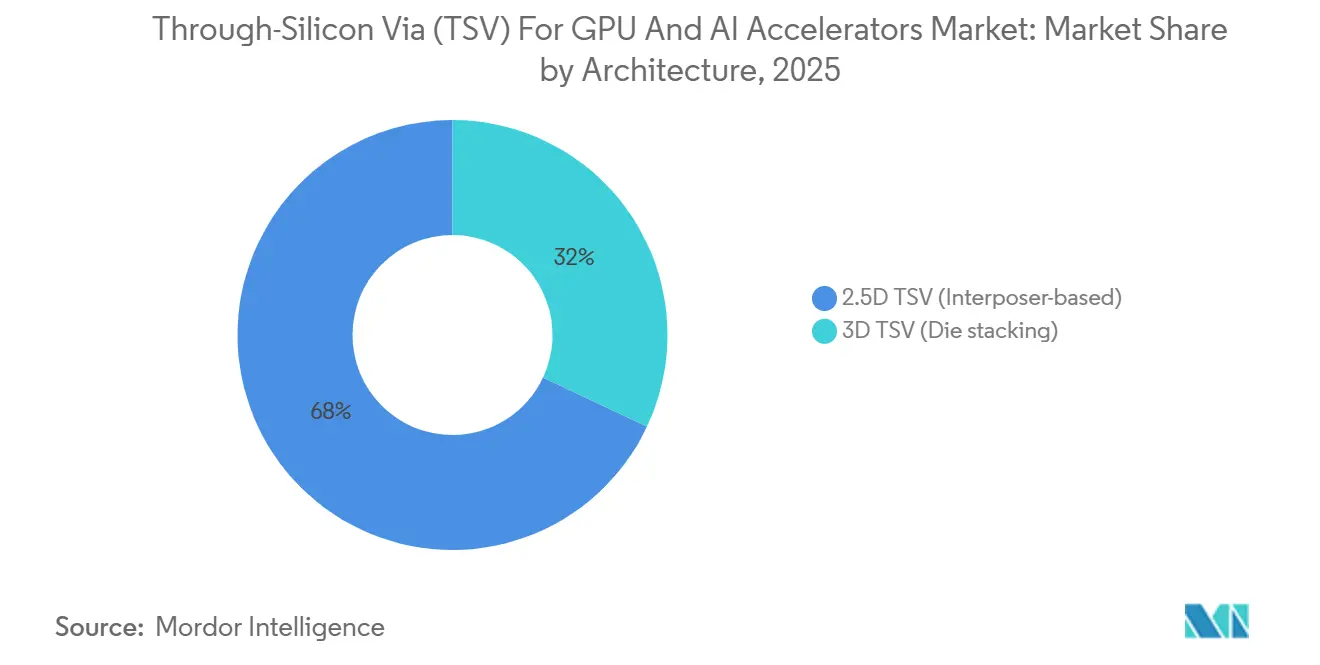
- By architecture, the 2.5D TSV interposer-based segment captured 68% of the Through-Silicon Via market share for GPU and AI accelerators in 2025, while the 3D TSV die-stacking segment is projected to grow at a 23.56% CAGR through 2031.
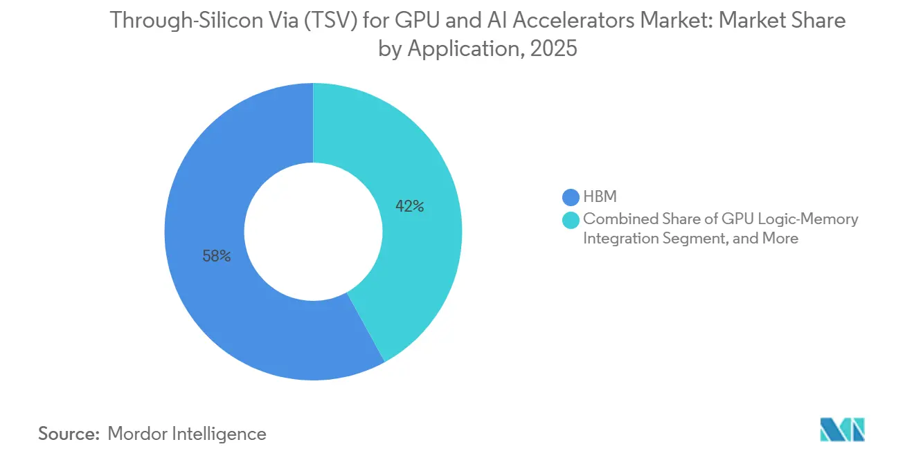
- By application, HBM memory stacks held 58% of the Through-Silicon Via for GPU and AI accelerators market size in 2025, whereas chiplet-based GPU architectures are expected to post the fastest 23.78% CAGR over 2026-2031.
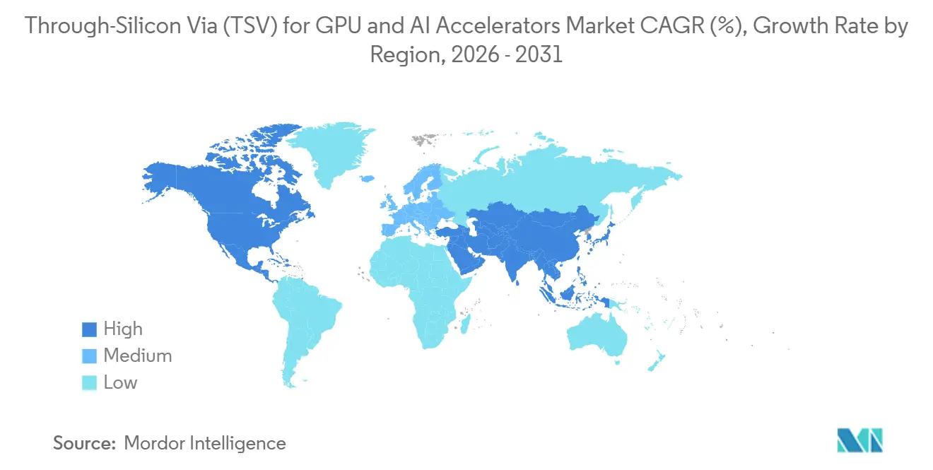
- By geography, Asia-Pacific accounted for 62% of the Through-Silicon Via for GPU and AI accelerators market share in 2025, and North America is forecast to record the fastest 24.15% CAGR through 2031.
Note: Market size and forecast figures in this report are generated using Mordor Intelligence’s proprietary estimation framework, updated with the latest available data and insights as of January 2026.
Global Through-Silicon Via (TSV) For GPU and AI Accelerators Market Trends and Insights
Drivers Impact Analysis*
| Driver | (~) % Impact on CAGR Forecast | Geographic Relevance | Impact Timeline |
|---|---|---|---|
| Mainstream Adoption of HBM3 and Beyond in AI GPUs | +6.8% | Global, Asia-Pacific manufacturing, North America deployment | Medium term (2-4 years) |
| Growth of Chiplet-Based GPU Designs Requiring Advanced Interposers | +5.2% | Global, North America design, Asia-Pacific fabrication | Medium term (2-4 years) |
| Increasing Capital Investments in 2.5D and 3D Packaging Facilities | +4.5% | Asia-Pacific core, North America expansion | Long term (≥ 4 years) |
| Government Incentives for Domestic Semiconductor Supply Chains | +3.1% | North America, Europe | Long term (≥ 4 years) |
| Emerging Hybrid Bonding TSV Techniques for Performance Boost | +2.4% | Taiwan, South Korea, United States | Long term (≥ 4 years) |
| Rising Demand for Energy-Efficient Data Center Accelerators | +1.9% | North America and Europe hyperscale operators | Medium term (2-4 years) |
| Source: Mordor Intelligence | |||
Mainstream Adoption of HBM3 and Beyond in AI GPUs
HBM3E and HBM4 are lifting TSV density targets above 100,000 vias per package, which redefines packaging cost structures and process windows. SK hynix validated 12-layer HBM4 samples exceeding 2 Tbit-s bandwidth and plans mass production in late 2025. NVIDIA’s Rubin GPU, disclosed in 2026, integrates 288 GB of HBM4 and relies on 16-layer stacks that still fit existing server z-height limits because Samsung demonstrated a 12-layer 3D-TSV package that maintains the 720 µm profile of legacy 8-layer HBM2. Memory vendors are now outsourcing base-die logic to leading-edge logic foundries, increasing TSV alignment tolerances and copper-to-copper bonding requirements. These changes are rapidly scaling the Through-Silicon Via market for GPU and AI accelerators as suppliers race to deliver reliable, high-aspect-ratio vias.
Growth of Chiplet-Based GPU Designs Requiring Advanced Interposers
Disaggregating monolithic GPUs into chiplets improves die yield and speeds product refreshes. AMD’s MI300A combines 5 nm compute tiles, 6 nm IO tiles, and HBM3 on a single CoWoS-S interposer and delivers over 5 TB-s memory bandwidth. Intel pushed sub-10 µm hybrid-bond pitch with Foveros Direct, enabling vertically stacked voltage regulators and logic layers. The Universal Chiplet Interconnect Express standard, co-led by Samsung, published an open die-to-die PHY in 2024, making interposer access less proprietary. These advances expand demand for large silicon interposers, boosting the Through-Silicon Via market for GPU and AI accelerators.
Increasing Capital Investments in 2.5D and 3D Packaging Facilities
Foundries and OSATs earmarked more than USD 20 billion for advanced packaging between 2024 and 2026. TSMC is committed to a USD 165 billion United States expansion plan that reserves capacity for CoWoS lines in Arizona. Amkor is building a USD 7 billion facility in Peoria to provide turnkey 2.5D and 3D services. Samsung and Tokyo Electron likewise stepped up capex for hybrid bonding and bonding equipment. The capital influx secures long-term growth for the Through-Silicon Via market for GPU and AI accelerators.
Government Incentives for Domestic Semiconductor Supply Chains
Public funding is catalyzing non-Asian packaging build-outs. The U.S. CHIPS and Science Act earmarked USD 39 billion in grants, including a dedicated advanced-packaging program.[1]U.S. Department of Commerce, “CHIPS for America,” CHIPS.GOV Intel secured USD 8.5 billion to expand Ohio and Arizona fabs with 3D packaging lines. The EU Chips Act set aside EUR 43 billion (USD 48.6 billion) for similar aims. Such incentives underwrite regional hubs, diversifying the footprint of the Through-Silicon Via market for GPU and AI accelerators.
Restraints Impact Analysis*
| Restraint | (~) % Impact of CAGR Forecast | Geographic Relevance | Impact Timeline |
|---|---|---|---|
| Yield Challenges in High-Density TSV Fabrication | -2.8% | Global, acute below 5 nm logic | Short term (≤ 2 years) |
| Thermal Management Limitations in Stacked GPU Modules | -1.9% | Global, most severe above 500 W | Medium term (2-4 years) |
| Supply Chain Vulnerabilities to Specialty TSV Equipment | -1.4% | Global, risk in lithography and bonding tools | Medium term (2-4 years) |
| Availability of Alternative Advanced Packaging | -0.8% | Global, fan-out and UCIe bridges | Long term (≥ 4 years) |
| Source: Mordor Intelligence | |||
Yield Challenges in High-Density TSV Fabrication
TSV aspect ratios now exceed 10:1 with diameters below 5 µm, stressing etch, fill, and reveal steps. IEEE research showed that TSV-induced stress shifts transistor thresholds, forcing the use of keep-out zones that erode silicon area.[2]IEEE, “TSV-Induced Stress Effects,” IEEE.ORG Chipmetrics’ inline void detection identified latent failures caused by copper voiding after thermal cycling. Applied Materials released a plasma-wet TSV reveal module that strips dielectric residue without copper damage to raise near-term yields. Until such fixes mature, production output for Through-Silicon Via for GPU and AI accelerators market devices remains gated by defect density.
Thermal Management Limitations in Stacked GPU Modules
Integrating >500 W logic dies with 12-layer HBM generates heat fluxes surpassing 200 W-cm². Imec's modeling identified a temperature difference of 15-20 °C between the top and bottom DRAM layers, leading to memory throttling. Projections indicate that socket power could reach 1,000 W by 2027, putting significant pressure on existing air- and single-phase liquid-cooling systems. While material advancements like SK hynix’s MR-MUF molding help reduce warpage, they fail to address vertical thermal pathways. Cooling limitations restrict operating frequency improvements, constraining the Through-Silicon Via for GPU and AI accelerators market until package-integrated cold plates and two-phase cooling solutions become viable.
*Our forecasts treat driver/restraint impacts as directional, not additive. The impact forecasts reflect baseline growth, mix effects, and variable interactions.
Segment Analysis
By Architecture: Interposers Dominate While Hybrid Bonding Scales
The 2.5D TSV interposer segment held 68% of the Through-Silicon Via market share for GPU and AI accelerators in 2025, driven by mature design rules and established substrate ecosystems. TSMC’s CoWoS-S supports interposers approaching 2,700 mm², accommodating multiple GPU chiplets and eight or more HBM cubes on one substrate. Samsung’s I-CubeE blends silicon bridges with fan-out redistribution layers to lower the cost for large-area interposers. These proven routes ensure high tape-out velocity and predictable yield, sustaining the segment’s scale in the Through-Silicon Via market for GPU and AI accelerators during the early forecast years.
3D die-stacking, though only 32% of the 2025 value, is growing at 23.56% CAGR as hybrid copper bonding enables sub-4 µm vertical pitch. Intel’s Foveros Direct and Samsung’s X-Cube target fine-pitch copper-to-copper joints that trim via parasitics and shorten interlogic paths. TSMC’s SoIC promises sub-1 µm pitch, useful for SRAM-on-logic stacks in future GPUs. As equipment yields improve, the 3D route is expected to capture incremental Through-Silicon Via market share for the GPU and AI accelerator market, tied to ultrahigh-bandwidth memory fabrics.


By Application: HBM Leads, Chiplet GPUs Accelerate
HBM stacks accounted for 58% of the total spending in 2025, driven by the widespread adoption of high-bandwidth memory in top-tier AI accelerators. Each of these accelerators incorporates at least six HBM3E cubes, highlighting the critical role of HBM technology in advancing AI performance. Micron’s 8 Gb-s-pin HBM3E ramp has been instrumental in supporting the launches of NVIDIA H200 and AMD MI300X, two of the most prominent AI accelerators in the market.[3]Micron, “HBM3E,” MICRON.COM Additionally, advancements in TSV (Through-Silicon Via) density have enabled Samsung to deliver 12-layer packages while maintaining the legacy 720 µm height. This innovation ensures that system designers can continue to operate within existing thermal envelopes, avoiding the need for significant redesigns.
Chiplet-based GPU architectures, while contributing only 17% of revenue in 2025, are projected to grow at an impressive CAGR of 23.78% through 2031. AMD’s MI300A is a prime example of cost-efficient scaling through compute tiles, showcasing the potential of chiplet technology to optimize performance and cost. Similarly, Intel’s Ponte Vecchio, which integrates more than 40 tiles, demonstrates the extreme degree of disaggregation enabled by chiplet-based designs. The adoption of smaller dies not only improves yield but also offers greater flexibility in the mixing process nodes. These advantages are driving increased customer adoption, significantly expanding the market size for Through-Silicon Via technology in GPU and AI accelerators, particularly in applications involving chiplet GPUs.

Geography Analysis
Asia-Pacific dominated the Through-Silicon Via for GPU and AI accelerators market in 2025 with a 62% revenue share, driven by TSMC, Samsung, and SK Hynix's cluster fabrication, advanced packaging, and HBM output in Taiwan and South Korea. TSMC’s Kumamoto R&D center in Japan co-locates substrate and materials partners, tightening supply cycles for CoWoS roadmap updates. Tokyo Electron scaled 2025 R&D spend to JPY 250.0 billion (USD 1.61 billion) to accelerate the release of bonding equipment and reinforce the regional ecosystem. Export-control headwinds limit China’s ability to secure advanced lithography, constraining domestic TSV capacity and limiting its local share of the Through-Silicon Via market for GPU and AI accelerators.
North America’s forecast CAGR of 24.15% is driven by hyperscaler demand and government subsidies. TSMC’s multi-fab Arizona campus reserves CoWoS lines for U.S. GPU customers, while Amkor’s Peoria plant brings an OSAT alternative onshore. Intel’s CHIPS-backed Ohio and Arizona expansions promise captive and merchant 3D packaging volumes. The increasing investments in U.S. data-center infrastructure, with AI accelerators emerging as the fastest-growing spend category, are further amplifying domestic demand.
Europe captures a modest but rising share thanks to the EUR 43 billion (approximately USD 46.44 billion) EU Chips Act pool, which finances pilot lines for wafer-level bonding and RDL interposers.[4]European Commission, “EU Chips Act,” EUROPA.EU STMicroelectronics, GlobalFoundries, and IMEC collaborate on heterogeneous integration test lines, but the absence of a local HBM supply continues to push European GPU designers to Asian memory vendors. South Am, the Middle East End Africa remain marginal, hosting only legacy back-end operations without TSV capacity.

Competitive Landscape
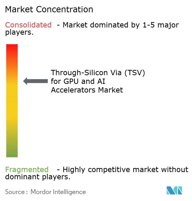
The Through-Silicon Via (TSV) market for GPU and AI accelerators is moderately concentrated, with a few key players dominating the landscape. TSMC commands an estimated 60-70% of the 2.5D interposer revenue through its CoWoS portfolio. This dominance is attributed to its ability to provide single-vendor accountability for logic and packaging fan-out-on-substrate solutions, a feature highly preferred by fabless GPU designers. Samsung, on the other hand, leverages its X-Cube hybrid bonding and I-CubeE fan-out interposers to attract customers who are dissatisfied with TSMC's lead times. However, Samsung's limited share in leading-edge logic somewhat restricts its market penetration. Intel is also making strides in this space by pursuing vertical integration. Its Foveros Direct lines cater to both internal accelerators and emerging Foundry clients, although concerns over internal prioritization have slowed external tape-outs.
OSATs, including ASE Technology, Amkor, and JCET, are scaling their operations by licensing CoWoS-equivalent flows or co-developing fan-out on substrates. These companies are playing a crucial role in expanding the market's capacity and addressing the growing demand for advanced packaging solutions. Equipment makers like Tokyo Electron and Applied Materials are also influencing the market's trajectory. Tokyo Electron’s Synapse Si and Applied Materials’ TSV reveal modules are pivotal in advancing the technology, as sub-4 µm bonding becomes a prerequisite for HBM4. These developments highlight the importance of collaboration across the supply chain to meet the evolving requirements of the GPU and AI accelerators market.
The Universal Chiplet Interconnect Express Consortium is another significant player shaping the market dynamics. By specifying open PHYs, the consortium aims to reduce foundry lock-in and foster a multi-sourced interposer market. This initiative could potentially disrupt the existing market structure, providing more flexibility and options for industry players. Meanwhile, proponents of fan-out technology argue that TSMC's InFO with through-InFO vias can meet bandwidth requirements at a lower cost, posing a challenge to TSV incumbents. The competitive landscape will ultimately depend on whether the yield, thermal, and bandwidth advantages of TSVs can outpace the cost efficiencies offered by large-panel fan-out technologies.
Through-Silicon Via (TSV) For GPU and AI Accelerators Industry Leaders
TSMC
Samsung Electronics
SK Hynix
Micron Technology
ASE Technology Holding
- *Disclaimer: Major Players sorted in no particular order

Recent Industry Developments
- April 2026: Applied Materials introduced a plasma-plus-wet TSV reveal module and sub-2 nm hybrid-bond surface-prep tools to reduce defectivity in high-aspect-ratio vias.
- February 2026: Tokyo Electron raised FY 2026 operating-profit guidance to JPY 593 billion (USD 3.8 billion) on surging sales of wafer-bonding and debonding systems tied to HBM lines.
- January 2026: SK hynix showcased 16-layer 48 GB HBM4 modules with TSMC-fabricated base dies at the TSMC Technology Symposium 2026.
- January 2026: NVIDIA unveiled its Rubin platform featuring 288 GB HBM4 per GPU packaged on CoWoS-S for 2027 production.


Global Through-Silicon Via (TSV) For GPU and AI Accelerators Market Report Scope
The Through-Silicon Via (TSV) for GPU and AI Accelerators Market refers to the global ecosystem involved in the development, manufacturing, and deployment of TSV-based semiconductor technologies that enable high-density vertical interconnections in advanced computing chips. TSV technology allows for direct electrical connections through silicon wafers or dies, supporting high-bandwidth, low-latency data transfer critical for modern graphics processing units (GPUs) and AI accelerators.
The Through-Silicon Via for GPU and AI Accelerators Market Report is Segmented by Architecture (2.5D TSV Interposer-based, and 3D TSV Die Stacking), Application (HBM Memory Stacks, GPU Logic-Memory Integration, AI Accelerators and HPC GPUs, and Chiplet-based GPU Architectures), and Geography (North America, Europe, Asia-Pacific, South America, and Middle East and Africa). The Market Forecasts are Provided in Terms of Value (USD).
| 2.5D TSV (Interposer-based) |
| 3D TSV (Die stacking) |
| HBM Memory Stacks |
| GPU Logic-Memory Integration |
| AI Accelerators / HPC GPUs |
| Chiplet-based GPU Architectures |
| North America | United States |
| Canada | |
| Mexico | |
| Europe | United Kingdom |
| Germany | |
| France | |
| Rest of Europe | |
| Asia-Pacific | China |
| Japan | |
| India | |
| South Korea | |
| Rest of Asia-Pacific | |
| South America | |
| Middle East and Africa |
| By Architecture | 2.5D TSV (Interposer-based) | |
| 3D TSV (Die stacking) | ||
| By Application | HBM Memory Stacks | |
| GPU Logic-Memory Integration | ||
| AI Accelerators / HPC GPUs | ||
| Chiplet-based GPU Architectures | ||
| By Geography | North America | United States |
| Canada | ||
| Mexico | ||
| Europe | United Kingdom | |
| Germany | ||
| France | ||
| Rest of Europe | ||
| Asia-Pacific | China | |
| Japan | ||
| India | ||
| South Korea | ||
| Rest of Asia-Pacific | ||
| South America | ||
| Middle East and Africa | ||


Key Questions Answered in the Report
What is the current size of the Through-Silicon Via for GPU and AI accelerators market and how fast is it growing?
The market stood at USD 8.37 billion in 2025, is expected to reach USD 11.54 billion in 2026, and is projected to climb to USD 32.69 billion by 2031 at a 23.15% CAGR.
Why are 2.5D interposers still dominant over fully stacked 3D architectures?
Mature design rules, proven reliability, and compatibility with established substrate ecosystems keep 2.5D interposers more economical for high-volume GPUs, whereas 3D die-stacking still battles yield and thermal hurdles.
How do government incentives influence TSV capacity build-outs?
U.S. CHIPS and EU Chips Act subsidies cover billions in grants and loan guarantees, accelerating construction of advanced-packaging lines and diversifying TSV production beyond Asia.
What are the main technical restraints facing TSV adoption in AI accelerators?
High-density TSV fabrication yields, heat dissipation in stacked GPU-HBM modules, and supply risk for specialty etch and bonding tools remain the leading bottlenecks.
Which companies supply the critical equipment for TSV and hybrid bonding?
Tokyo Electron, Applied Materials, and Lam Research dominate wafer-to-wafer bonding, TSV etch, and reveal processes that underpin high-volume HBM production.
How will chiplet standards like UCIe affect the competitive landscape?
Open die-to-die interface standards can lower switching costs and invite more foundry and OSAT competition, potentially eroding proprietary advantages of current TSV market leaders.
Page last updated on: