
2.5D and 3D IC Packaging For AI Accelerators Market Size and Share
Market Overview
| Study Period | 2020 - 2031 |
|---|---|
| Market Size (2026) | USD 11.24 Billion |
| Market Size (2031) | USD 45.19 Billion |
| Growth Rate (2026 - 2031) | 32.09 % |
| Fastest Growing Market | North America |
| Largest Market | Asia-Pacific |
| Market Concentration | High |
Major Players *Disclaimer: Major Players sorted in no particular order Image © Mordor Intelligence. Reuse requires attribution under CC BY 4.0. | |
2.5D and 3D IC Packaging For AI Accelerators Market Analysis by Mordor Intelligence
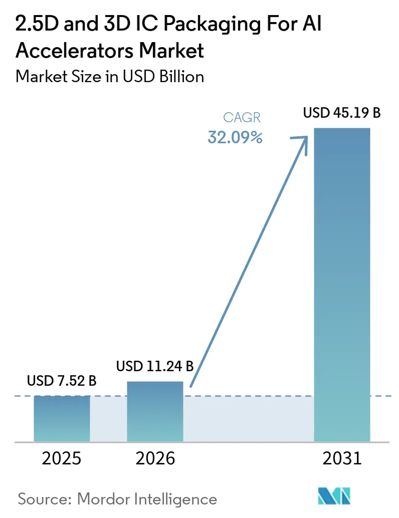
The 2.5D and 3D IC packaging market size is projected to be USD 7.52 billion in 2025, USD 11.24 billion in 2026, and reach USD 45.19 billion by 2031, growing at a 32.09% CAGR over 2026-2031. The jump tracks the semiconductor pivot from monolithic die scaling to heterogeneous integration, a shift magnified by foundation-model compute demand. Foundries and outsourced assembly and test (OSAT) houses are racing to add hybrid bonding lines, sub-10 µm micro-bump lithography, and redistribution-layer interposers that can sustain 10 TB/s die-to-die bandwidth. Capital intensity is unprecedented; Taiwan Semiconductor Manufacturing Company (TSMC) alone set a 2026 capex range of USD 52 billion-USD 56 billion, a large share of which will fund CoWoS capacity aimed at 150,000 wafers per month. Government incentives reinforce the build-out; the United States earmarked USD 1.6 billion for advanced packaging grants, while Japan and South Korea launched multi-billion-dollar subsidy programs. Generative-AI training drives the bulk of today’s demand, yet inference and enterprise on-premise clusters are the fastest-rising use cases. NVIDIA’s Blackwell GPUs, AMD’s MI350 series, and Intel’s Gaudi 3 all rely on CoWoS-L or Foveros Direct packages that couple logic tiles and HBM3E stacks at pitches under 25 µm, slashing latency while boosting bandwidth fivefold over prior generations. Tight supply, lingering yield limits above 8-high HBM, and export controls on sub-10 µm bonding tools create persistent bottlenecks, giving top foundries a pricing edge yet pulling OSATs such as ASE Technology and Amkor into margin-squeezing capex cycles. Even so, growing chiplet ecosystems under Universal Chiplet Interconnect Express (UCIe) 2.0 are widening customer choice, lowering vendor lock-in risk, and accelerating multi-die adoption across geographic clusters.
Key Report Takeaways
- By packaging technology, 2.5D IC packaging led with 88% revenue share in 2025, while 3D IC packaging is advancing at a 32.49% CAGR through 2031.
- By packaging platform, CoWoS held a dominant 69% share in 2025, whereas Foveros and EMIB solutions are set to expand at a 32.89% CAGR over 2026-2031.
- By application, AI training accelerators accounted for 57% of 2025 sales, yet AI inference accelerators are forecast to grow at a 32.77% CAGR through 2031.
- By end user, hyperscalers and cloud providers captured 73% share in 2025, while enterprise AI infrastructure is projected to log a 32.91% CAGR during 2026-2031.
- By geography, Asia-Pacific dominated with 65% market share in 2025, whereas North America is poised to rise at a 33.09% CAGR through 2031.
Note: Market size and forecast figures in this report are generated using Mordor Intelligence’s proprietary estimation framework, updated with the latest available data and insights as of January 2026.
Market Trends and Insights
Drivers Impact Analysis of 2.5D and 3D IC Packaging For AI Accelerators Market*
| Driver | (~) % Impact on CAGR Forecast | Geographic Relevance | Impact Timeline |
|---|---|---|---|
| Exploding Training Compute Requirements in Foundation Models | +8.2% | Global – North America and Asia-Pacific hyperscale data centers | Medium term (2-4 years) |
| Rapid AI Accelerator Refresh Cycles in Cloud Data Centers | +7.5% | Global – led by North America hyperscalers and Asia-Pacific cloud providers | Short term (≤ 2 years) |
| Heterogeneous Integration Roadmaps of Leading Foundries | +6.8% | Asia-Pacific (Taiwan, South Korea, Japan), North America (United States) | Long term (≥ 4 years) |
| Government Funding for Advanced Packaging Capacity Expansion | +4.3% | North America, Europe, Asia-Pacific | Medium term (2-4 years) |
| Sustainability Push Toward Lower-Power Chiplet Architectures | +2.9% | Global – EU regulatory influence | Long term (≥ 4 years) |
| Vertical AI Start-Ups Demanding Custom 3D Packages | +2.4% | North America, Europe | Short term (≤ 2 years) |
| Source: Mordor Intelligence | |||
Exploding Training Compute Requirements in Foundation Models
Training runs now exceed 10²⁵ floating-point operations, one hundred times the 2020 benchmark. OpenAI needed 25,000 NVIDIA A100 GPUs for GPT-4, while Meta’s 405 billion-parameter Llama 3.1 consumed over 16,000 H100S.[1] These clusters saturate HBM3E bandwidth before tensor cores reach full utilization, forcing architects to adopt 2.5D interposers like CoWoS-L that furnish 10 TB/s die-to-die bandwidth. Dual-die GPUs also let suppliers salvage partially yielding tiles, boosting overall wafer economics. As researchers eye 10-trillion-parameter models by 2027, packaging will remain the prime lever for meeting bandwidth and power-delivery demands.
Rapid AI Accelerator Refresh Cycles in Cloud Data Centers
Hyperscalers are cutting accelerator refresh intervals from two years to one. Microsoft rolled out Maia 200 across Azure in late 2025, Google began TPU v8 volume shipments in 2025, and AWS introduced Trainium 2 in 2024. Each SKU demands packaging that mixes logic, memory, and analog I/O dies in a single footprint. Latency-sensitive inference variants increasingly favor vertical stacking, nudging suppliers toward hybrid bonding. Lead times for CoWoS lines are 6 to 9 months, so long-term foundry alliances become decisive for allocation.
Heterogeneous Integration Roadmaps of Leading Foundries
Foundries now market packaging nodes alongside lithography nodes. TSMC groups CoWoS-S, CoWoS-L, and CoWoS-R under its 3DFabric umbrella and is lifting its capacity to 150,000 wafers per month by end-2026. Intel’s Foveros Direct pushes 10 µm bump pitch with hybrid bonding, slices package thickness by 30%, and cuts parasitic capacitance by 40%. Samsung’s I-Cube series offers modular variants that lower the entry hurdle for fabless designers. Standardized UCIe 2.0 links now let designers mix chiplets from multiple vendors, catalyzing broader heterogeneous integration.
Government Funding for Advanced Packaging Capacity Expansion
The United States CHIPS and Science Act reserved USD 1.6 billion solely for packaging and substrates, with Absolics, Applied Materials, and Arizona State University among early grantees. Japan committed JPY 920 billion (USD 6.3 billion) to expand TSMC’s Kumamoto site, and South Korea rolled out a KRW 26 trillion (USD 19.4 billion) package for Samsung and SK hynix. These subsidies diversify geographic risk and shorten supply chains but also intensify localized talent wars.
Restraints Impact Analysis of 2.5D and 3D IC Packaging For AI Accelerators Market*
| Restraint | (~) % Impact on CAGR Forecast | Geographic Relevance | Impact Timeline |
|---|---|---|---|
| Yield Management Challenges Beyond 8-High HBM Stacks | -3.8% | South Korea, Taiwan | Short term (≤ 2 years) |
| Limited Sub-10 µm Micro-Bump Supply Chain Readiness | -2.9% | Taiwan, Japan, United States | Medium term (2-4 years) |
| CapEx Intensity Straining OSAT Profitability | -2.1% | Taiwan, China, South Korea | Medium term (2-4 years) |
| Geopolitical Export Controls on Advanced Packaging Tools | -1.7% | China – secondary impact globally | Long term (≥ 4 years) |
| Source: Mordor Intelligence | |||
Yield Management Challenges Beyond 8-High HBM Stacks
SK hynix’s 12-high HBM3E brings 36 GB per package yet faces alignment tolerances under 1 µm and warpage over 50 µm during reflow, cutting yields to the low-50% range.[2] Samsung plans to counter with hybrid bonding for HBM4 in 2026, but that process tightens surface-roughness specs to sub-nm levels and heightens particulate sensitivity. TSMC’s CoWoS-L yields reach 70%-80% at 8-high yet dip below 50% at 12-high, doubling the cost per functional package. Until backside power delivery and new underfill chemistries mature, large-capacity stacks will remain cost-challenged.
Limited Sub-10 µm Micro-Bump Supply Chain Readiness
Applied Materials’ Endura Copper Barrier Seed system targets a 5 µm pitch but ships in limited numbers with 12-month lead times. Tokyo Electron’s Telios lithography tool and KLA’s LS-9800 inspection platform carry eight-figure price tags and nine-month delivery slots. Few OSATs can finance the purchases, so TSMC, Samsung, and Intel enjoy an 18-month lead. Shortages are slowing hybrid bonding ramp-ups and keeping CoWoS day rates elevated, squeezing second-tier suppliers.
*Our forecasts treat driver/restraint impacts as directional, not additive. The impact forecasts reflect baseline growth, mix effects, and variable interactions.
2.5D and 3D IC Packaging For AI Accelerators Market Segment Analysis
By Packaging Technology:
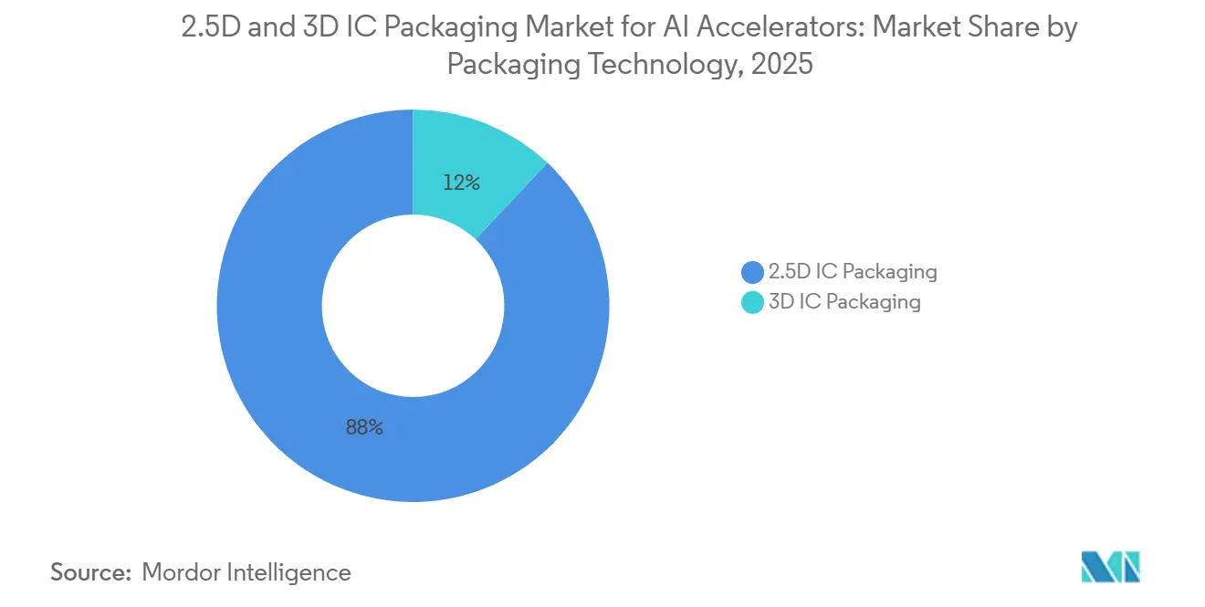
2.5D Dominates as 3D Gains Speed2.5D IC packaging accounted for 88% of 2025 revenue, aided by CoWoS shipments to NVIDIA Blackwell GPUs. The 2.5D and 3D IC packaging market size for 2.5D solutions is anchored by multi-reticle silicon interposers that integrate logic tiles with up to eight HBM stacks. Still, 3D IC packaging is forecast to grow at a 32.49% CAGR, as vertical stacking collapses signal paths by 90% and unlocks backside power delivery. Intel’s Meteor Lake processors show 20% energy gains through PowerVia-enabled Foveros Direct, and Samsung’s X-Cube roadmap rivals that performance. Over the next five years, AI inference at the edge and thermal budgets under 500 W will push designers toward 3D topologies that minimize footprint and latency.
Adoption hurdles remain. 3D assembly requires known-good-die testing at each layer and tighter wafer-to-wafer alignment, slowing throughput compared with 2.5D interposer bonding. Yield drag persists for stacks with more than 4 active logic layers, yet suppliers are co-optimizing die design, wafer thinning, and thermal-compression steps to boost line productivity. As these kinks ease, 3D’s share of the overall 2.5D and 3D IC packaging market is set to double by 2031, even as 2.5D interposers retain primacy for memory-bound training GPUs that need massive lateral area.
By Packaging Platform:
CoWoS Holds Sway amid Foveros and EMIB ExpansionCoWoS secured 69% market share in 2025, fueled by NVIDIA, AMD, and multiple hyperscaler custom chips. The 2.5D and 3D IC packaging market share commanded by CoWoS reflects early learning-curve advantages and front-end integration with TSMC’s 4 nm and 3 nm nodes. Yet Intel’s EMIB and Foveros lines are logging a 32.89% CAGR, helped by Gaudi 3, Ponte Vecchio, and external foundry customers. EMIB embeds a silicon bridge within an organic laminate, slashing package cost by 40% compared to full-area interposers. Foveros stacks dies at 10 µm pitch, cutting latency for inference workloads that prize millisecond responsiveness.
Samsung’s I-Cube introduces modular H-Cube, S-Cube, and X-Cube variants, positioning the Korean firm as a strong alternative in memory-centric designs. OSAT offerings such as Amkor SWIFT and ASE FOCoS target cost-sensitive edge AI markets where package thickness and bill-of-materials costs trump absolute bandwidth. Over time, platform diversity will allow designers to mix interposer, bridge, and fan-out modalities, selecting the lowest-cost architecture that meets workload needs.
By Application:
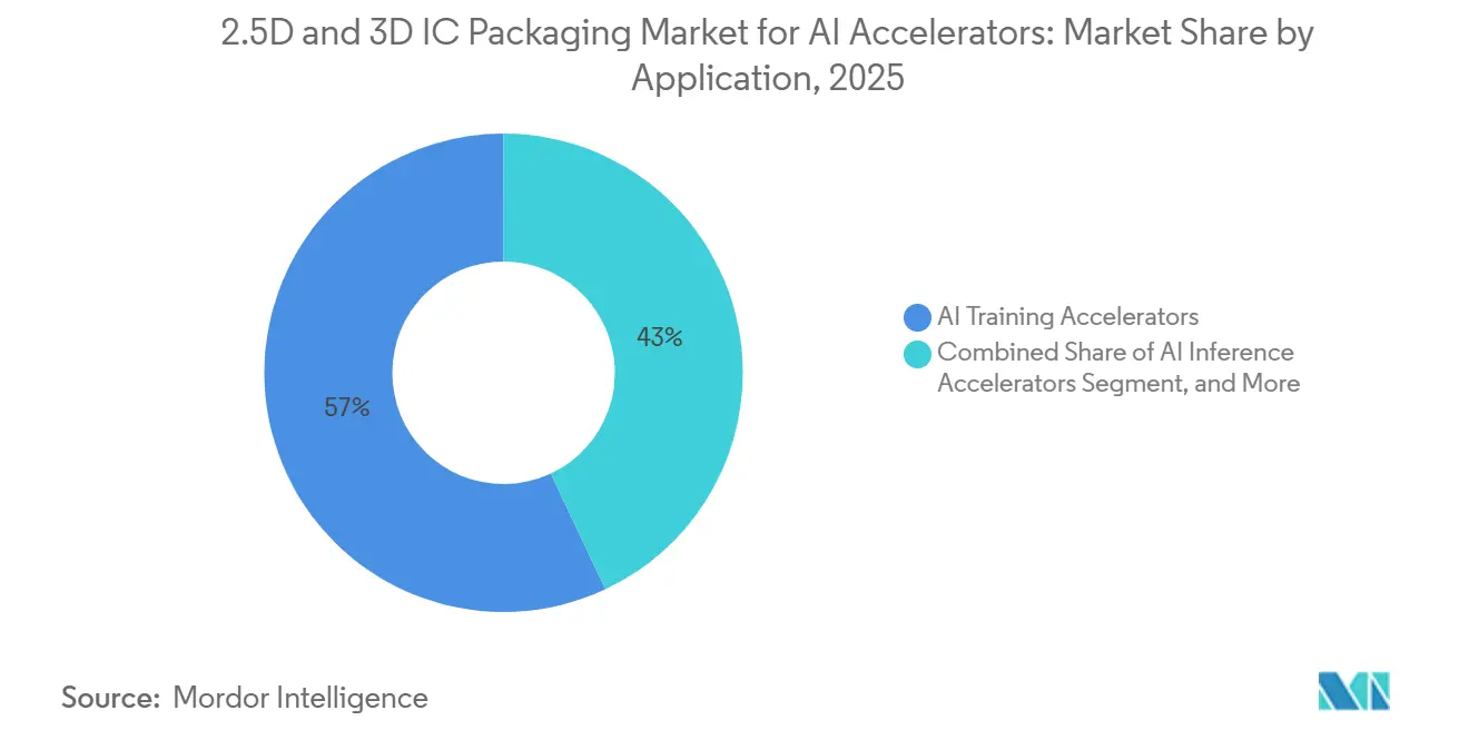
Training Leads, Inference AcceleratesAI training accelerators accounted for 57% of 2025 revenue, as hyperscalers poured capex into foundation-model clusters. CoWoS-L packages with 10 TB/s bandwidth are now table stakes for models with more than one trillion parameters. However, inference accelerators are poised for a 32.77% CAGR, driven by the monetization of ChatGPT-like services and the rise of edge deployments in autonomous vehicles and industrial IoT. The 2.5D and 3D IC packaging market size tied to inference will widen as power envelopes shrink and latency targets tighten, giving 3D stacked logic-memory designs an edge.
High-performance computing (HPC) accelerators, while occupying a smaller portion of the market, continue to serve as critical platforms for innovation. Products like AMD’s MI325X, which features 256 GB of HBM3E memory on a 2.5D interposer, and Intel’s Ponte Vecchio, comprising 47 tiles, exemplify hybrid approaches that integrate training, inference, and HPC design requirements. These technologies enable cross-pollination of ideas and advancements across different applications. Furthermore, insights from areas such as thermal management and yield control are shared across segments, significantly accelerating learning and development cycles within the industry.

By End User:
Hyperscalers Dominate, Enterprises Catch UpHyperscalers and cloud providers owned 73% of 2025 demand, thanks to vertical integration and deep wallets that secure long-term CoWoS allocations. The 2.5D and 3D IC packaging market is still capacity-constrained; TSMC’s lines are booked through 2026, leaving smaller customers scrambling for slots. Nonetheless, enterprise AI infrastructure is forecast to post a 32.91% CAGR because data-sovereignty rules and cost-of-ownership math push private-cloud and on-premise deployments. Dell and Hewlett-Packard Enterprise now bundle liquid-cooled MI300 and H100 nodes, easing adoption hurdles for non-hyperscaler buyers.
Research institutes and government HPC centers contribute to diversifying the high-performance computing landscape, though their procurement cycles tend to be longer than those in other sectors. Notable examples include Frontier at Oak Ridge National Laboratory and Aurora at Argonne National Laboratory, both of which utilize 2.5D packaged GPUs to achieve exascale computing capabilities. These systems serve as critical benchmarks for government-supported artificial intelligence (AI) initiatives worldwide, showcasing the potential of advanced HPC technologies to drive innovation and support large-scale computational needs.
Geography Analysis
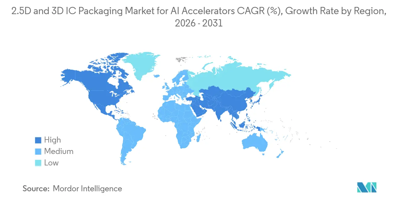
APAC 2.5D and 3D IC Packaging for AI Accelerators Market
Asia-Pacific captured 65% of 2025 revenue, driven by Taiwan’s dominance in CoWoS technology and South Korea’s leadership in HBM production. TSMC is investing between USD 52 billion and USD 56 billion in capital expenditures through 2026, with plans to achieve a production capacity of 150,000 CoWoS wafers per month. Meanwhile, Samsung has announced a record-breaking USD 73 billion capital expenditure plan for 2026, with a significant portion allocated to hybrid-bonded HBM4 production lines. Additionally, Japan has provided a JPY 920 billion (USD 6.3 billion) subsidy for TSMC’s Kumamoto site, establishing a second major hub in Asia and reducing reliance on a single geographic location.
North America 2.5D and 3D IC Packaging for AI Accelerators Market
North America is projected to be the fastest-growing region, with a compound annual growth rate (CAGR) of 33.09%. This growth is fueled by USD 1.6 billion in CHIPS Act packaging grants and Intel’s Ohio fabrication complex, which integrates front-end lithography with advanced back-end technologies such as Foveros and EMIB.[3] Furthermore, Applied Materials’ new research center in Sunnyvale, California, and Absolics’ glass-substrate manufacturing facility in Georgia are helping to streamline critical-materials supply chains within the region.
EMEA and South America 2.5D and 3D IC Packaging for AI Accelerators Market
Europe’s market share remains relatively modest; however, the EUR 43 billion (USD 47 billion) European Chips Act is now supporting the development of pilot packaging lines in Germany and France. In contrast, South America, the Middle East, and Africa are lagging but are actively pursuing OSAT partnerships to support the production of automotive and industrial chips. Early initiatives, such as Brazil’s Ceitec and the UAE’s Mubadala-backed ventures, are making progress, though large-scale interposer manufacturing capacity is expected to remain concentrated in Asia and North America through 2031.
Competitive Landscape
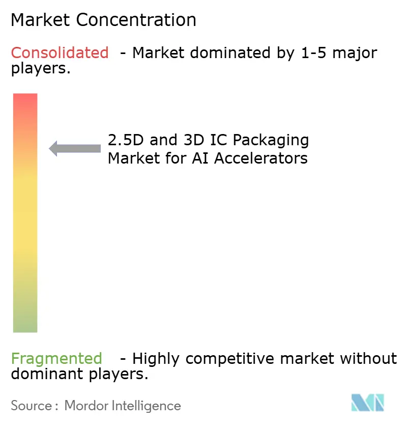
Market concentration is moderate. TSMC, Samsung, and Intel collectively dominate approximately 75% of advanced packaging capacity, yet Outsourced Semiconductor Assembly and Test (OSAT) providers are steadily narrowing the gap. ASE Technology reported TWD 159.9 billion (USD 4.96 billion) in revenue for Q3-2024; however, its gross margin declined as the company scaled up production of FOCoS and CoWoS-like lines to meet growing demand. Meanwhile, Amkor is making significant strides by committing USD 2 billion to establish a fan-out plant in Arizona.[4] This strategic investment aims to attract U.S.-based hyperscalers, reduce their reliance on Taipei's production queues, and strengthen Amkor's market position.
Emergent players are addressing market gaps by introducing innovative solutions. Cerebras, for instance, has eliminated the need for interposers with its wafer-scale WSE-3, which integrates an impressive 900,000 cores into a single reticle. Similarly, Tenstorrent is leveraging chiplet meshes connected via UCIe 2.0, which necessitates the development of bespoke high-density bridges. These cutting-edge architectures are compelling suppliers to innovate by creating custom substrates and advanced thermal-interface materials, thereby expanding their solution portfolios to cater to these new demands.
Geopolitical factors are significantly influencing competition within the industry. In 2026, the United States Bureau of Industry and Security extended export controls to include hybrid-bonding equipment, further restricting China's access to sub-10 µm bump-pitch technology. As a result, domestic Chinese OSAT providers, such as JCET, have shifted their focus to 20-µm fan-out lines. This strategic pivot has delayed their ability to compete in the advanced CoWoS-equivalent segment by at least 18 months, highlighting the challenges posed by these regulatory measures.
2.5D and 3D IC Packaging For AI Accelerators Industry Leaders
-
Taiwan Semiconductor Manufacturing Company Limited
-
Intel Corporation
-
ASE Technology Holding Co. Ltd.
-
Samsung Electronics Co. Ltd.
-
Amkor Technology Inc.
- *Disclaimer: Major Players sorted in no particular order
2.5D and 3D IC Packaging For AI Accelerators Market Companies Covered in this Report
- Taiwan Semiconductor Manufacturing Company Limited
- Samsung Electronics Co. Ltd.
- Intel Corporation
- ASE Technology Holding Co. Ltd.
- Amkor Technology Inc.
- United Microelectronics Corporation
- Powertech Technology Inc.
- Jiangsu Changjiang Electronics Technology Co. Ltd.
- Siliconware Precision Industries Co. Ltd.
- Advanced Micro Devices Inc.
- NVIDIA Corporation
- Broadcom Inc.
- Marvell Technology Inc.
- Xilinx Inc. (AMD)
- Graphcore Ltd.
- Tenstorrent Inc.
- Cerebras Systems Inc.
- Alibaba Group Holding Limited (T-Head)
- Huawei Technologies Co. Ltd. (HiSilicon)
- Google LLC (Tensor Processing Unit)
Recent Industry Developments in 2.5D and 3D IC Packaging For AI Accelerators Market
- April 2026: Samsung began building its P5 twin fab in Pyeongtaek, South Korea. The KRW 160 trillion (USD 119 billion) site targets HBM4 mass production with 12-high hybrid bonding by 2028.
- March 2026: Intel entered volume production of the Gaudi 3 accelerator using Foveros Direct packages at 10 µm pitch, priced 30% below comparable Blackwell GPUs.
- February 2026: TSMC secured a USD 6.6 billion syndicated loan to lift CoWoS capacity to 180,000 wafers per month by 2027.
- January 2026: The U.S. Bureau of Industry and Security broadened export controls to sub-10 µm advanced packaging tools.
Global 2.5D and 3D IC Packaging For AI Accelerators Market Report Scope
The 2.5D and 3D IC Packaging for AI Accelerators Market refers to the global industry that designs, manufactures, and integrates advanced semiconductor packaging technologies to enable high-performance artificial intelligence (AI) computing systems. These packaging approaches, primarily 2.5D interposer-based integration and full 3D die stacking, facilitate high-bandwidth, low-latency communication between processing units, memory (such as HBM), and other chiplets, making them essential for modern AI accelerators.
The 2.5D and 3D IC Packaging for AI Accelerators Market Report is Segmented by Packaging Technology (2.5D IC Packaging, and 3D IC Packaging), Packaging Platform (CoWoS, I-Cube, Foveros and EMIB, and Other Custom Advanced Packaging Platforms), Application (AI Training Accelerators, AI Inference Accelerators, and HPC Accelerators), End-User (Hyperscalers and Cloud Providers, Enterprise AI Infrastructure, and Research and Government AI and HPC Centers), and Geography (North America, Europe, Asia-Pacific, South America, and Middle East and Africa). The Market Forecasts are Provided in Terms of Value (USD).
Segmentation Overview
| 2.5D IC Packaging |
| 3D IC Packaging |
| CoWoS |
| I-Cube |
| Foveros / EMIB |
| Other Custom Advanced Packaging Platforms |
| AI Training Accelerators |
| AI Inference Accelerators |
| HPC Accelerators |
| Hyperscalers / Cloud Providers |
| Enterprise AI Infrastructure |
| Research and Government AI/HPC Centers |
| North America | United States |
| Canada | |
| Mexico | |
| Europe | United Kingdom |
| Germany | |
| France | |
| Rest of Europe | |
| Asia-Pacific | China |
| Japan | |
| India | |
| South Korea | |
| Rest of Asia-Pacific | |
| South America | |
| Middle East and Africa |
| By Packaging Technology | 2.5D IC Packaging | |
| 3D IC Packaging | ||
| By Packaging Platform | CoWoS | |
| I-Cube | ||
| Foveros / EMIB | ||
| Other Custom Advanced Packaging Platforms | ||
| By Application | AI Training Accelerators | |
| AI Inference Accelerators | ||
| HPC Accelerators | ||
| By End-User | Hyperscalers / Cloud Providers | |
| Enterprise AI Infrastructure | ||
| Research and Government AI/HPC Centers | ||
| By Geography | North America | United States |
| Canada | ||
| Mexico | ||
| Europe | United Kingdom | |
| Germany | ||
| France | ||
| Rest of Europe | ||
| Asia-Pacific | China | |
| Japan | ||
| India | ||
| South Korea | ||
| Rest of Asia-Pacific | ||
| South America | ||
| Middle East and Africa | ||
Key Questions Answered in the Report
What is the current 2.5D and 3D IC packaging market size and its expected value by 2031?
The market stands at USD 11.24 billion in 2026 and is forecast to reach USD 45.19 billion by 2031, reflecting a 32.09% CAGR .
Which packaging platform holds the largest share today?
CoWoS leads with 69% of 2025 revenue, thanks to entrenched use in GPUs and hyperscaler custom ASICs.
Why is 3D IC packaging growing faster than 2.5D?
Vertical stacking cuts latency and footprint, pairs well with backside power delivery, and aligns with inference workloads that require compact, low-power form factors.
How will UCIe affect chiplet adoption?
The open standard enables multi-vendor chiplet ecosystems, reducing lock-in and accelerating heterogeneous integration across compute, memory, and I/O dies.
Which region is projected to grow the fastest through 2031?
North America, boosted by USD 1.6 billion in CHIPS Act subsidies, is set to post a 33.09% CAGR for advanced packaging.
What are the main technical hurdles facing HBM stack scaling?
Yield management past 8-high stacks and limited supply of sub-10 µm micro-bump and hybrid-bonding tools slow cost-effective deployment of 12-high and 16-high configurations.