
Thin Film Encapsulation Market Size and Share
Market Overview
| Study Period | 2020 - 2031 |
|---|---|
| Market Size (2026) | USD 0.42 Billion |
| Market Size (2031) | USD 1.06 Billion |
| Growth Rate (2026 - 2031) | 20.22 % |
| Fastest Growing Market | Middle East and Africa |
| Largest Market | Asia Pacific |
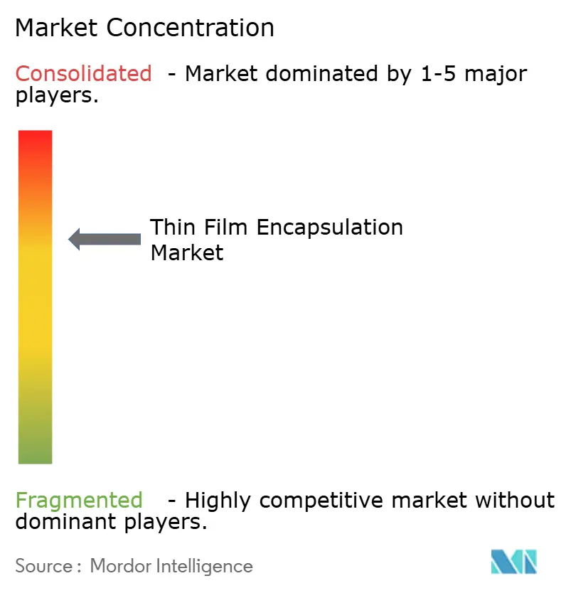
| Market Concentration | Medium |
Major Players *Disclaimer: Major Players sorted in no particular order Image © Mordor Intelligence. Reuse requires attribution under CC BY 4.0. | |
Thin Film Encapsulation Market Analysis by Mordor Intelligence
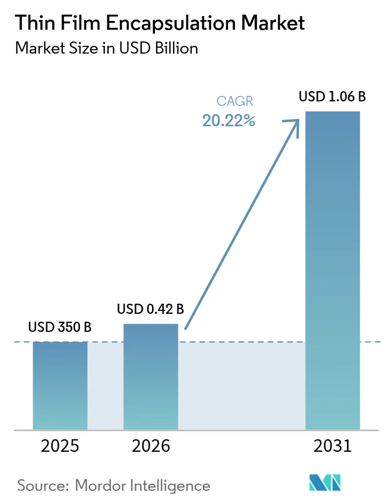
Thin film encapsulation market size in 2026 is estimated at USD 420.77 million, growing from 2025 value of USD 350 million with 2031 projections showing USD 1.06 billion, growing at 20.22% CAGR over 2026-2031. Rapid adoption of flexible OLED displays, surging demand for bendable consumer devices, and aggressive capacity additions in Asia-Pacific have kept the growth trajectory steep. Manufacturers are prioritizing atomic layer deposition (ALD) barriers that achieve water-vapor transmission rates below 10⁻⁶ g/m²/day, enabling longer device lifetimes while preserving form-factor flexibility. Automotive mandates for curved cockpit displays and medical certification of roll-to-roll ALD films are widening application scope, even as precursor shortages and capital-intensive Gen-6 ALD lines present headwinds. Competitive intensity is rising as Chinese firms, buoyed by “New Display” subsidies, scale output and erode Korean dominance.[1]Chae-Yeon Kim, “Samsung ups smaller OLED workforce to fend off Chinese rivals,” KED Global, kedglobal.com
Key Report Takeaways
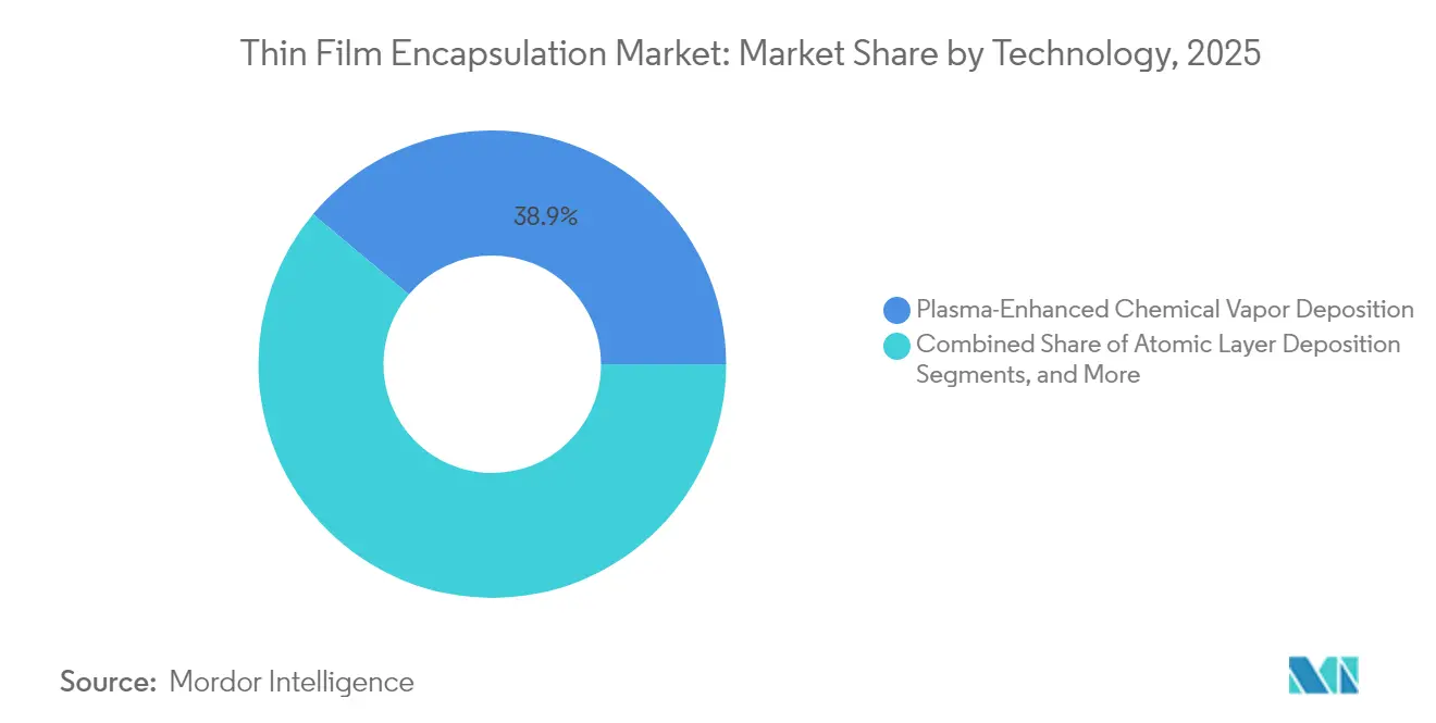
- By technology, plasma-enhanced chemical vapor deposition led with 38.90% of the thin film encapsulation market share in 2025, while ALD is advancing at 25.85% CAGR through 2031.
- By layer structure, hybrid multi-layer barriers accounted for 46.85% of the thin film encapsulation market size in 2025; single-layer solutions are expanding at 28.35% CAGR.
- By application, flexible OLED displays held 60.95% revenue share in 2025, whereas automotive displays and lighting post the fastest 31.95% CAGR to 2031.
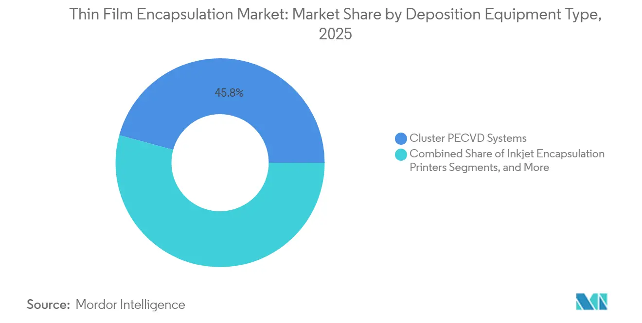
- By deposition equipment type, cluster PECVD systems captured 45.75% share of the thin film encapsulation market size in 2025; ALD reactors mark the quickest 33.10% CAGR.
- By end-use industry, consumer electronics dominated with a 73.90% share in 2025, while healthcare and wearables registered a 30.05% CAGR by 2031.
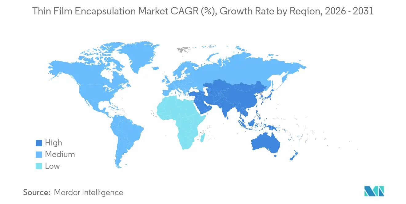
- By geography, Asia-Pacific commanded 69.10% of the thin film encapsulation market share in 2025; the Middle East and Africa region is projected to climb at 26.35% CAGR between 2026-2031.
Note: Market size and forecast figures in this report are generated using Mordor Intelligence’s proprietary estimation framework, updated with the latest available data and insights as of 2026.
Market Trends and Insights
Drivers Impact Analysis of Thin Film Encapsulation Market*
| Driver | (~) % Impact on CAGR Forecast | Geographic Relevance | Impact Timeline |
|---|---|---|---|
| AMOLED capacity expansions in South Korea and China | +5.2% | Asia-Pacific, spillover to North America | Medium term (2-4 years) |
| Automotive curved-display mandates in the EU and NA | +4.8% | Europe, North America | Medium term (2-4 years) |
| Roll-to-roll ALD unlocking certified medical wearables | +3.9% | Global, early uptake in North America and Europe | Long term (≥ 4 years) |
| EU carbon-neutral BIPV push boosting inorganic barriers | +2.6% | Europe, spillover to North America | Long term (≥ 4 years) |
| SID award-winning low-temp ALD enabling foldables | +2.4% | Global, early adoption in Asia-Pacific | Short term (≤ 2 years) |
| China “New Display” subsidies covering encapsulation CapEx | +2.1% | Asia-Pacific | Short term (≤ 2 years) |
| Source: Mordor Intelligence | |||
AMOLED capacity expansions in South Korea and China are fueling ALD-TFE tool orders
Samsung Display allocated USD 3 billion for an 8.6-generation IT OLED line targeting 2026 production, while BOE committed USD 8.7 billion for a comparable plant. These projects multiplied purchase orders for ALD encapsulation tools because the technology offers uniform, pinhole-free barriers at low temperatures, a necessity for next-generation IT and automotive panels. Heightened competition has revived Korean shipment leadership but simultaneously broadened ALD demand across Asia-Pacific foundries.
Automotive curved-display mandates in the EU and North America
Regulatory guidance favoring seamless instrument clusters has sparked accelerated design-ins of curved OLED dashboards. These modules need encapsulation stacks that withstand vibration, UV exposure, and -40 °C cycling. Samsung’s adoption of tandem OLED with advanced moisture barriers exemplified the shift, positioning the firm to capture revenue as total automotive display spend is forecast to overtake monitor panel sales by 2026.
Roll-to-roll ALD unlocking certified medical wearables
Pilot web lines achieved detection-limit water-vapor transmission rates at 0.25 m/min coating speed, enabling textiles that remain operational after bending, washing, and prolonged skin contact. Such performance satisfied global medical approval pathways, opening mass production of e-textiles for continuous vital-sign monitoring.
EU carbon-neutral BIPV push boosting inorganic barriers
The EU Strategic Research and Innovation Agenda prioritized long-life building-integrated photovoltaics, forcing module makers to adopt ALD-based inorganic barriers that secure 25-year lifetimes against moisture and UV stress. Demand for transparent, durable coatings is consequently rising in Europe’s construction supply chain.
Restraints Impact Analysis of Thin Film Encapsulation Market*
| Restraint | (~) % Impact on CAGR Forecast | Geographic Relevance | Impact Timeline |
|---|---|---|---|
| High CapEx of Gen-6 ALD cluster lines | -3.1% | Global, highest in emerging markets | Medium term (2-4 years) |
| Reliability failures under −40 °C automotive cycling | -2.3% | Europe, North America | Short term (≤ 2 years) |
| Competition from ultra-thin flexible glass | -1.8% | Global | Long term (≥ 4 years) |
| Precursor supply bottlenecks (e.g., DEZ) | -1.5% | Global, highest in Asia-Pacific | Short term (≤ 2 years) |
| Source: Mordor Intelligence | |||
High CapEx of Gen-6 ALD cluster lines
Next-generation ALD stacks demand more than USD 100 million per line, sidelining mid-tier producers and slowing technology diffusion. Many Asian fabs still amortize older cluster tools, complicating upgrade economics even where yield benefits are clear. This cost barrier delays uniform adoption of best-in-class encapsulation across the thin film encapsulation market.
Reliability failures under −40 °C automotive cycling
Delamination and crack propagation in hybrid barriers remain common when panels face rapid thermal cycling from cabin heat to winter cold. Failures expose organic layers to moisture, curtailing display lifespan. Ongoing material research and development now integrates stress-release organics, but at a premium manufacturing cost, tempering automotive revenue expansion.
*Our forecasts treat driver/restraint impacts as directional, not additive. The impact forecasts reflect baseline growth, mix effects, and variable interactions.
Thin Film Encapsulation Market Segment Analysis
By Technology:
ALD drives next-level barrier integrityALD recorded a 25.85% CAGR outlook while PECVD held 38.90% revenue in 2025, illustrating a transition phase within the thin film encapsulation market. ALD films reached water-vapor rates at 10⁻⁶ g/m²/day that extend OLED life spans and support foldable substrates. Roll-to-roll ALD upgraded throughput to web speeds suitable for wearable production, while spatial ALD is overcoming substrate-size limits. PECVD remains preferred for rigid panels needing high volume. VTE and OVPD continue in niche emissive stacks where material compatibility overrides barrier extremity. Low-temperature ALD chemistries awarded by SID in 2023 unlocked polyimide substrates for mass foldables, deepening the technology mix. Consequently, ALD tool providers enjoy record order backlogs, lifting regional supplier ecosystems across South Korea, China, and the United States.
The thin film encapsulation market continues to rely on PECVD for cost-sensitive SKUs because the reactors integrate seamlessly with legacy TFT lines. Inkjet encapsulation printing, spearheaded by Kateeva, decreased organic material waste and enabled patterned barriers for smartwatch dials. VTE retains relevance for small-area microdisplays where device yield trumps throughput. With spatial ALD crossing 15 gen substrates in pilot tests, the competitive landscape between PECVD and ALD is expected to tighten, driving hybrid production floors that leverage both methods.



By Layer Structure:
hybrids maintain dominance while single-layer surgesHybrid stacks combining parylene C with ALD Al₂O₃ secured 46.85% sales in 2025, thanks to a proven balance of stress relief and moisture blocking. These dyads achieved sub-10⁵ g/m²/day WVTR while sustaining flex cycles exceeding 10,000 bends, a specification demanded by premium smartphones. Single-layer barriers, however, now post the fastest 28.35% CAGR because silbione-blended hybrimer films offer comparable protection at half the deposition sequence length, cutting takt time for rollable panels.
Inorganic multi-layers deliver unmatched oxygen resistance but risk crack formation under tensile stress, limiting adoption in foldables. Organic multi-layers excel in bendability yet rarely reach lifetime targets alone. Commercial lines consequently calibrate layer architecture by product class: smartphones accept hybrid dyads, automotive clusters need triple inorganic caps, while e-textiles increasingly lean on advanced organic chemistries. Component suppliers respond with modular material kits that harmonize refractive index, modulus, and stickiness across adjoining layers, ensuring line reliability beyond 90% yield.
By Application:
flexible displays prevail as vehicles accelerateFlexible OLEDs captured 60.95% of 2025 revenue within the thin film encapsulation market. Their dominance stemmed from major smartphone and notebook launches that mandated sub-10⁵ g/m²/day barriers without adding bulk thickness. Commercial foldables extended panel lifetime beyond 200,000 opens when paired with hybrid dyads, validating mass retail readiness.
Automotive displays represent the most explosive application with a 31.95% CAGR. Curved dashboards and transparent HUD modules require tandem OLED stacks plus resilient encapsulation, a niche that Samsung, LG Display, and BOE aggressively pursued through bespoke tooling contracts. MicroLED and quantum-dot integrations are emerging; encapsulation pockets produced via maskless lithography shield each sub-pixel isotropically, promising 8K HDR clusters for AR and cockpit usage. Thin-film solar modules, printable sensors, and wearables also absorb barrier innovation, but at smaller absolute volumes.
By Deposition Equipment Type:
cluster PECVD retains volume leadershipCluster PECVD tools generated 45.75% of 2025 equipment sales owing to their high-throughput capability and compatibility with existing fab layouts. Integrated load-lock and transfer arms minimized particle risk, boosting panel yield for rigid TVs and monitors. Meanwhile, ALD reactors expanded by 33.10% CAGR as spatial reactor designs improved wafer-equivalent per hour counts threefold, challenging PECVD cost equations.
Inkjet encapsulation printers addressed material wastage by depositing organics only where needed, lowering the bill of materials in smartwatch lines. Roll-to-roll vacuum systems became crucial for e-textile and sensor webs where substrate lengths exceed 300 m. Laser-assisted repair stations, though niche, salvaged defective large-area panels, improving overall equipment effectiveness. Vendors increasingly bundle software analytics, enabling predictive maintenance, elevating uptime expectations in hyper-competitive fabs.
By End-Use Industry:
consumer electronics dominates, healthcare risesSmartphones, tablets, and notebooks formed 73.90% of the thin film encapsulation market revenue in 2025 as flagship models shifted from rigid to flexible AMOLED. Fierce competition among handset OEMs pushed display makers to secure best-in-class barriers, reinforcing continuous investments in ALD and hybrid organic films.
Healthcare and wearables, though smaller, observe a 30.05% CAGR because ultrathin barriers enable skin-compatible patches and implantable sensors requiring impermeability over multi-year service lives. Automotive adoption outpaces the overall panel market, while renewable-energy modules benefit from ALD caps that prolong outdoor reliability. Industrial and aerospace niches specify the toughest barrier metrics, often commanding premium margins and specialized service contracts.
Geography Analysis
APAC Thin Film Encapsulation Market
Asia-Pacific retained 69.10% revenue share in 2025, driven by South Korea’s and China’s fab expansions and integrated supply ecosystems. Government incentives covering encapsulation capital costs accelerated ALD cluster installations, while Korean players pivoted toward high-value products and tandem stacks to defend margins. Regional tooling and chemical suppliers co-located near fabs, shortening qualification cycles and reinforcing dominance across the thin film encapsulation market.
Europe Thin Film Encapsulation Market
Europe posted healthy gains built on automotive and BIPV demand. Strict EU vehicle safety directives accelerated curved OLED cockpit adoption, and carbon-neutral building rules spurred ALD barrier uptake in solar façades. Research consortia advanced low-temperature ALD precursors, aligning performance with circular-economy objectives.
MEA Thin Film Encapsulation Market
The Middle East and Africa exhibited the highest 26.35% CAGR outlook from a small base, as nations like the UAE and Saudi Arabia funded electronics clusters to diversify their economies. Harsh desert climates necessitated robust encapsulation for display and solar products, creating premium demand for ALD-based inorganic layers. Technology transfer partnerships with Asian OEMs seeded local capacity, reducing single-region dependency for global brands.
North America Thin Film Encapsulation Market
North America maintained influence through materials science leadership and equipment exports despite limited panel production. Automotive mandates and quantum-dot microLED research and development anchored demand for specialized barrier know-how, while roll-to-roll ALD startups leveraged venture funding to commercialize wearable lines. Regional fabs collaborated with universities on machine-learning process control, enhancing film uniformity and throughput.

Regulatory Landscape
Thin film encapsulation demand and supply are shaped by electronics, chemicals, and industrial policy regimes. In Europe, Regulation (EU) 2023/1781 (EU Chips Act) sets a framework to strengthen secure semiconductor ecosystems, influencing where advanced deposition and encapsulation capabilities are supported and qualified in the region. In China, the State Administration for Market Regulation issued GB/T 45939-2025 in August 2025 as a reference standard for films used in thin-film module encapsulation, reinforcing standardization in barrier-film performance and compatibility for downstream photovoltaic and flexible electronics applications.
Trade and chemical compliance requirements also affect tool and material availability. In the United States, the Bureau of Industry and Security revised license review policy for exports of certain semiconductors to China and Macau in January 2026 under the Export Administration Regulations, adding friction for cross-border movement of advanced semiconductor items that can include enabling deposition equipment and related supply chains. Material compliance continues to track EU RoHS amendments and related exemption status monitoring, as reflected in supplier declarations such as Taiwan Semiconductor compliance updates aligned to Commission Delegated Directives (EU) 2025/2363 and (EU) 2025/1802. In the United States, chemical oversight includes TSCA-related requirements referenced in 40 CFR 721.10888 for specific substances that can intersect with specialty precursors and polymer systems used around encapsulation workflows.
Value Chain Analysis
The thin film encapsulation value chain starts with high-purity chemical precursors and specialty materials, including inorganic oxides and nitrides for ALD/PECVD, organic barrier polymers, adhesion promoters, and compatible substrate films. It then moves through deposition equipment and process integration, where tool OEMs and integrators deliver ALD, PECVD, roll-to-roll vacuum systems, and inkjet encapsulation printers into display and flexible electronics fabs. Encapsulation stacks are co-optimized with OLED deposition, patterning, and inspection to meet ultra-low WVTR targets, down to 10^-6 g/m2/day in leading applications.
Qualification and reliability validation, especially for automotive temperature cycling and medical wearables, act as gating steps before volume ramps. Asia-Pacific anchors the ecosystem because panel makers, equipment vendors (for example, Applied Materials, Beneq, Veeco, and Kateeva), and specialty chemical suppliers co-locate near fab clusters, which reduces iteration time on defect control and yield. Key constraints in the chain include the high CapEx of Gen-6 ALD cluster lines, noted in the report as exceeding USD 100 million per line, limited high-throughput roll-to-roll ALD/PECVD capacity for large-area flexible substrates, and bottlenecks in ultra-clean, defect-free polymer substrates and select precursors such as DEZ. These constraints increase the importance of dual-sourcing strategies, tool-material co-development programs, and localized supply to shorten qualification cycles and reduce disruption risk.
Competitive Landscape
Market concentration was moderate as leading panel makers in South Korea and China vied for share, yet Western firms shaped material and tool innovation. China’s subsidies lowered entry barriers, prompting capacity waves and squeezing equipment lead times.
Strategic alliances tightened: Merck added low-temperature silicon materials under its liviFlex™ umbrella to pair with Applied Materials’ new ALD cluster platform, allowing joint tool-chemistry demonstrations at customer sites. LG Display partnered with an automaker on custom encapsulated OLED dashboards capable of surviving −40 °C cycling, reflecting vertically integrated solution selling.
White-space revenue emerged in medical wearables and microLED AR glasses. Specialists patented maskless lithography quantum-dot pockets to deliver isotropic sealing and fine patterning.[4]Resul Ozdemir et al., “Quantum dot patterning and encapsulation,” ACS Applied Materials and Interfaces, hal.umontpellier.fr Forge Nano showcased machine-learning ALD controls that slashed cycle times, a differentiator for high-mix fabs. As applications diversify, suppliers segment portfolios by end-market certification, possibly increasing fragmentation even while headline consolidation among tier-one panel makers persists.
Thin Film Encapsulation Industry Leaders
Samsung SDI Co.,Ltd.
Applied Materials, Inc.
Kateeva
Veeco Instruments Inc.
LG Chem Ltd.
- *Disclaimer: Major Players sorted in no particular order
Thin Film Encapsulation Market Companies Covered in this Report
- Samsung SDI Co., Ltd.
- LG Chem Ltd.
- Universal Display Corporation
- Applied Materials Inc.
- Veeco Instruments Inc.
- 3M Inc.
- Toray Industries Inc.
- Kateeva
- BASF (Rolic) AG
- Meyer Burger Technology AG
- Encapsulix SAS
- Forge Nano Inc.
- Aixtron SE
- Angstrom Engineering Inc.
- Forge Nano Inc.
- Beneq Oy
- Picosun Oy
- Canon Tokki Corporation
- AP Systems
- EMD Electronics (Merck KGaA)
- Idemitsu Kosan Co.
- Encapsulix SAS
- Wonik IPS
- Vitriflex Inc.

Market Opportunities and Future Outlook
Near-term whitespace is concentrated where encapsulation performance, mechanical durability, and qualification demands converge, particularly automotive curved cockpit displays and certified medical wearables highlighted in the report context. Automotive modules require barrier stacks that tolerate vibration, UV exposure, and -40 C cycling, which supports uptake of hybrid multi-layer architectures and tighter integration of encapsulation with display stack design. For medical and wearable electronics, roll-to-roll ALD pilot lines demonstrating very low WVTR at usable web speeds create a pathway to skin-contact and wash-resistant e-textiles. This shifts opportunities toward suppliers that can pair deposition capability with biocompatible material sets and documented reliability.
On the supply side, materials and process localization programs create openings for vendors supporting the broader encapsulation ecosystem around advanced thin films. In July 2026, Asahi Kasei completed a new slitting facility for SUNFORT dry film photoresist at Tainan, Taiwan, strengthening regional readiness for high-volume film handling and downstream patterning needs that often sit adjacent to encapsulation process flows in advanced manufacturing. Standardization also supports adoption beyond core display lines; China’s GB/T 45939-2025 for thin-film module encapsulation films provides a reference point for qualifying barrier films in thin-film PV and related flexible module use cases, expanding the addressable application set for inorganic and hybrid barrier suppliers without changing the report scope.
Recent Industry Developments in Thin Film Encapsulation Market
- June 2026: Applied Materials launched the Opta Quad platform and Producer Avila 2 PECVD system for advanced packaging and high-bandwidth memory stacking, targeting film stability and warpage control on ultra-thin dies. The release reinforces continued investment in precision thin-film deposition platforms that share process know-how and tool architectures with encapsulation-intensive manufacturing environments.
- February 2025: Applied Materials released a high-throughput ALD tool tuned for flexible-display encapsulation. By raising throughput on pinhole-free barrier deposition, the tool supports faster capacity ramps for flexible OLED lines that require very low water-vapor ingress rates.
- January 2024: Tianma Microelectronics ordered Kateeva's YIELDjet EXPLORE inkjet printing system to expand OLED display R&D, building on use of Kateeva's YIELDjet FLEX mass-production platform. The order underscores continued process development around inkjet-deposited encapsulation and adjacent functional layers to improve material utilization and enable patterned barrier concepts.


Thin Film Encapsulation Market Report Scope and Research Methodology
Market Definition and Coverage
For this methodology, the thin film encapsulation market covers thin, multilayer barrier stacks deposited on sensitive devices to protect them from moisture and oxygen, mainly for flexible electronics. We size the market as the value of thin film encapsulation materials and related deposition-driven solutions supplied for end-use manufacturing.
Scope exclusions: Excluded from sizing are rigid glass-only covers, discrete can packages, and stand-alone desiccant parts that are not part of a deposited thin-film barrier stack.
Segments Covered in This Report
- By Technology
- Plasma-Enhanced Chemical Vapor Deposition (PECVD)
- Atomic Layer Deposition (ALD)
- Inkjet Printing
- Vacuum Thermal Evaporation (VTE)
- Organic Vapor Phase Deposition (OVPD)
- Roll-to-Roll ALD
- Other Emerging Techniques (Parylene, Sol-Gel)
- By Layer Structure
- Inorganic Multilayer Barriers
- Organic Multilayer Barriers
- Hybrid (Organic+Inorganic) Barriers
- Single-Layer Encapsulation
- By Application
- Flexible OLED Displays
- Thin-Film Photovoltaics
- Flexible OLED Lighting
- Wearable and Medical Electronics
- Automotive Displays and Lighting
- Quantum-Dot and MicroLED Devices
- Printed Sensors and IoT Devices
- By Deposition Equipment Type
- Cluster PECVD Systems
- Inkjet Encapsulation Printers
- ALD Reactors
- Roll-to-Roll Vacuum Systems
- Laser-Assisted Deposition Tools
- By End-Use Industry
- Consumer Electronics
- Renewable Energy
- Automotive and Transportation
- Healthcare and Wearables
- Industrial and Aerospace
- By Geography
- North America
- United States
- Canada
- Mexico
- South America
- Brazil
- Argentina
- Rest of South America
- Europe
- Germany
- France
- United Kingdom
- Italy
- Rest of Europe
- Asia-Pacific
- China
- South Korea
- Japan
- India
- Rest of Asia-Pacific
- Middle East and Africa
- Middle East
- Saudi Arabia
- United Arab Emirates
- Turkey
- Rest of Middle East
- Africa
- South Africa
- Nigeria
- Rest of Africa
- Middle East
- North America
Data Sources, Market Sizing, and Validation
Desk Research
Desk work starts by mapping the demand pool for flexible electronics that rely on barrier performance, and then aligning it to how encapsulation is typically specified and purchased. We use public references such as the US International Trade Commission, UN Comtrade, the World Intellectual Property Organization patent data, and National Institute of Standards and Technology publications to ground definitions, process terms, and trade patterns. For OLED and photovoltaics context, we also review sources such as IEA PVPS outputs and SEMI and IEEE publications where they are openly accessible.
Next, company filings, investor presentations, earnings transcripts, and credible press coverage are used to track capacity additions, equipment spending cycles, and supply constraints that can affect delivered value in a given year. A paid subscription for company financials and intelligence is used selectively to standardize revenue splits and confirm corporate structures, and a patent database subscription helps check technology emphasis over time. This list of desk sources is illustrative, and many other public materials were also referred to for data collection, validation, and research clarification.
Primary Interviews and Surveys
Primary work is used to stress-test the desk model, especially on what buyers count as thin film encapsulation versus adjacent barrier or cover solutions, and on how pricing changes with stack complexity. We speak with a mix of material suppliers, equipment and process specialists, component makers, and device manufacturers across APAC, EMEA, and the Americas, so regional build-outs and adoption timing are reflected in the final numbers.
Distribution of primary research fieldwork respondents
| Company type | Respondent position | Region |
|---|---|---|
| Top tier: 26% | CXOs: 20% | APAC: 46% |
| Mid tier: 54% | Functional/Unit leaders: 20% | EMEA: 30% |
| Smaller Players: 20% | Managers: 60% | Americas: 24% |
Market-Sizing & Forecasting
Sizing begins with a top-down build that reconstructs thin film encapsulation demand from flexible OLED and other addressable production indicators, and then converts that demand into market value using realistic adoption and value-per-area assumptions. Inputs used in the model include flexible OLED panel output and ramp schedules, the share of devices using thin barriers instead of alternative sealing approaches, average barrier stack complexity (organic-inorganic pairs and target performance levels), usable yield and scrap factors during ramp-ups, and typical price progression tied to throughput and material utilization.
Results are then corroborated with selective bottom-up checks, such as sampled ASP times estimated coated area, supplier-side revenue band checks, and channel discussions on how deposition service value is packaged with materials. When company disclosures do not split thin film encapsulation clearly, gaps are handled by applying primary-validated allocation keys based on product mix and end-use exposure.
For forecasting, scenario analysis is used because adoption is driven by discrete capacity expansions and design wins, which can shift timing by a few quarters. Expert inputs are used to set realistic ramp curves and to align the outlook with known investment cycles in display and related flexible electronics.
Data Validation & Update Cycle
Outputs are checked against independent signals, including major capacity announcements, capex cycles in relevant manufacturing lines, and expected unit shipment trends for key flexible device categories. If a region or application shows an abrupt step change that is not supported by these signals, the assumptions are revisited and, when needed, selected interviewees are re-contacted to confirm what changed.
Before sign-off, the work goes through multi-step internal reviews that focus on logic consistency, unit sanity checks, and year-over-year variance. Reports are refreshed annually, and interim updates are made when material events occur, such as major line start-ups, policy changes, or supply constraints that shift pricing. Right before delivery, a final analyst pass is completed so clients receive the most current view available.
Mordor Intelligence's Thin Film Encapsulation Market Size Versus Other Published Estimates
It is normal to see different market values for thin film encapsulation because authors do not always count the same things, and they also use different timing for ramps, pricing, and currency conversion. In this market, the largest swings usually come from what gets bundled into the value number and whether the estimate follows display-led demand signals or uses broader electronics totals.
Some published figures bundle in adjacent packaging or protection items and then apply a single adoption rate across flexible devices. For Mordor Intelligence, the number is kept limited to deposited thin-film barrier stacks used for encapsulation, and adjacent rigid covers, discrete can packages, and stand-alone desiccants are excluded so the demand pool stays traceable to coating-driven usage and realistic ASP-by-stack assumptions.
Benchmark comparison
| Source | Market Size | Gaps in Research Methodology |
|---|---|---|
| Mordor Intelligence | USD 0.42 B (2026) | |
| Industry Database A | USD 0.13 B (2024) | Uses an earlier base year and a narrower priced scope that appears to focus on selective flexible OLED-related applications, which can undercount value added from broader adoption beyond core display use cases. |
| Industry Publisher B | USD 0.16 B (2025) | Uses a different base year and a longer forecast window, and the market value framing suggests alternate bundling rules around what is included in the encapsulation stack, leading to a structurally different starting point. |
The spread in the table mainly reflects year alignment and what is treated as part of the encapsulation solution versus adjacent protection components. By tying the model to clear demand indicators, realistic ramp behavior, and stack-level pricing logic, we keep the estimate explainable and repeatable even when public disclosures are limited.


Key Questions Answered in the Report
What is driving the rapid growth of the thin film encapsulation market?
High demand for flexible OLED displays, increased automotive adoption of curved dashboards, and rising medical wearable production are together pushing the market toward a 20.22% CAGR through 2031.
Which technology segment is expanding fastest within thin film encapsulation?
Atomic layer deposition is projected to grow at 25.85% CAGR because it delivers pinhole-free barriers at low temperatures suitable for foldable and automotive panels.
How significant is Asia-Pacific in thin film encapsulation manufacturing?
Asia-Pacific accounted for 69.10% of 2025 revenue, supported by large-scale fabs in South Korea and China and government incentives covering encapsulation equipment investments.
Why are single-layer barriers gaining traction despite hybrid dominance?
Material breakthroughs such as silbione-blended hybrimer films achieve ultra-low moisture rates while simplifying process steps, fueling a 28.35% CAGR for single-layer solutions.
What are the main constraints on thin film encapsulation adoption in automotive displays?
The report covers the Thin Film Encapsulation Market historical market size for years: 2019, 2020, 2021, 2022, 2023 and 2024. The report also forecasts the Thin Film Encapsulation Market size for years: 2026, 2027, 2028, 2029, 2030 and 2031.
Page last updated on:


 Your data is secure and never sold or shared.


