Semiconductor Packaging Market Size and Share
Market Overview
| Study Period | 2020 - 2031 |
|---|---|
| Market Size (2026) | USD 103.08 Billion |
| Market Size (2031) | USD 156.41 Billion |
| Growth Rate (2026 - 2031) | 8.70% CAGR |
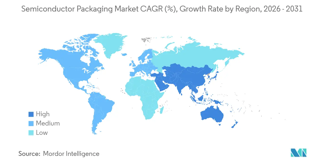
| Fastest Growing Market | Middle East |
| Largest Market | Asia Pacific |
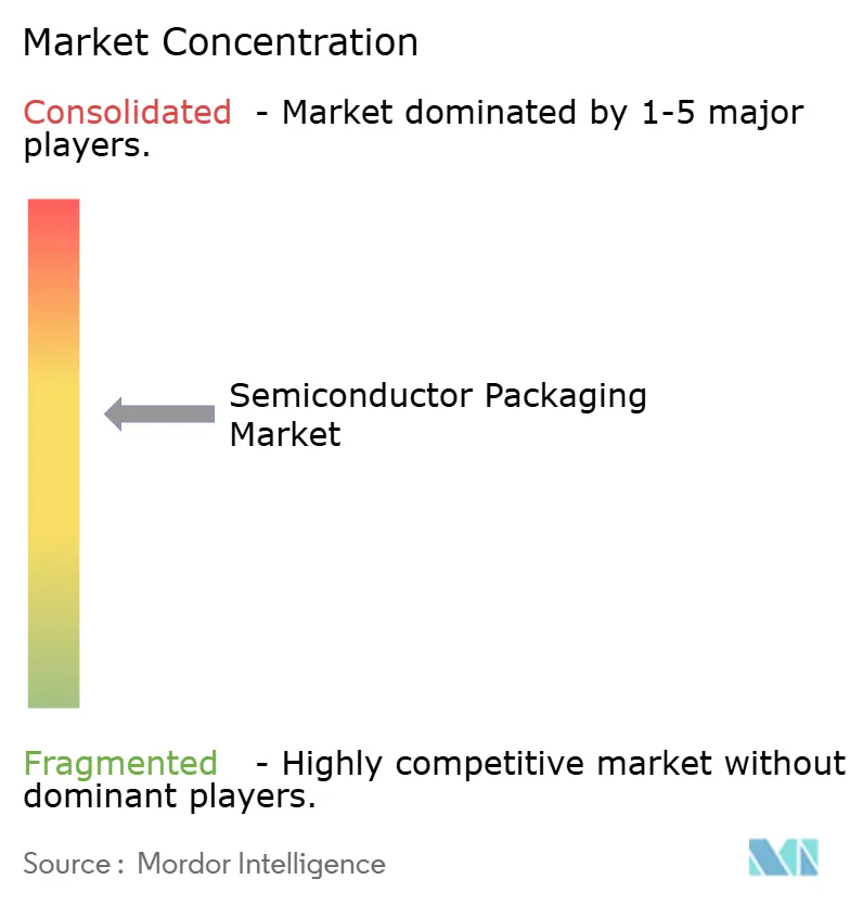
| Market Concentration | Medium |
Major Players *Disclaimer: Major Players sorted in no particular order Image © Mordor Intelligence. Reuse requires attribution under CC BY 4.0. | |
Semiconductor Packaging Market Analysis by Mordor Intelligence
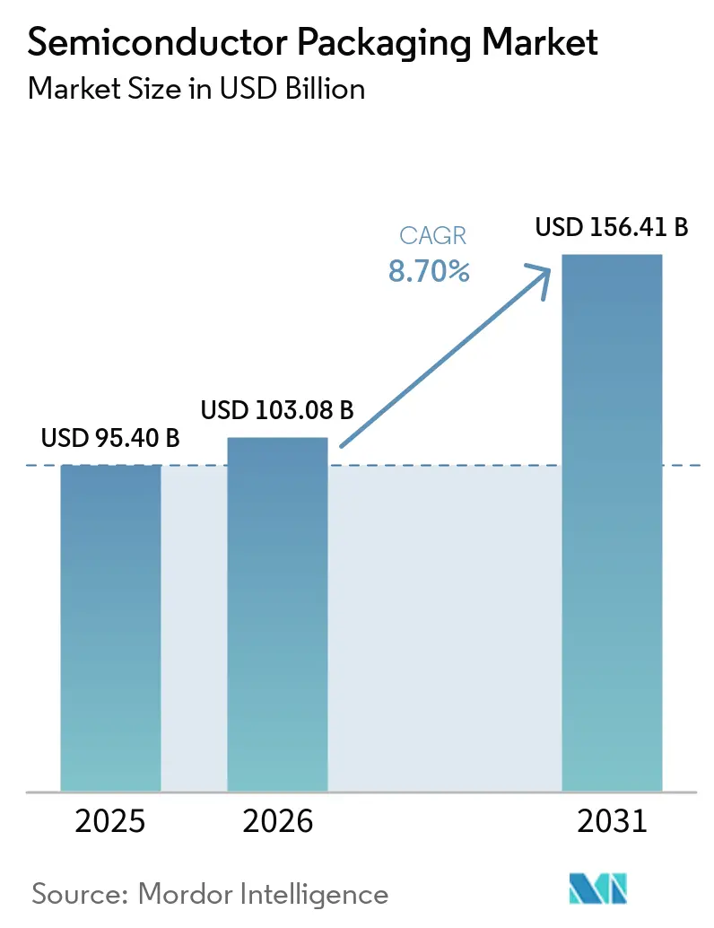
The Semiconductor Packaging Market size is projected to be USD 95.40 billion in 2025, USD 103.08 billion in 2026, and reach USD 156.41 billion by 2031, growing at a CAGR of 8.70% from 2026 to 2031.
Growth is propelled by hyperscale data-center demand for AI accelerators, rising electric-vehicle power requirements, and public incentives under the United States CHIPS and Science Act and the EU Chips Act. Capacity tightness in 2.5D/3D interposers has driven multi-year reservation contracts, while regional subsidies are redrawing traditional outsourcing maps. Meanwhile, substrate shortages, yield headwinds in hybrid bonding, and thermal limits in fan-out wafer-level packaging create counter-pressures that balance expansion with risk. Competitive strategies now revolve around backward integration by foundries, co-investment by hyperscalers, and accelerated adoption of standardized die-to-die interconnects, all of which collectively reshape the semiconductor packaging market trajectory.
Key Report Takeaways
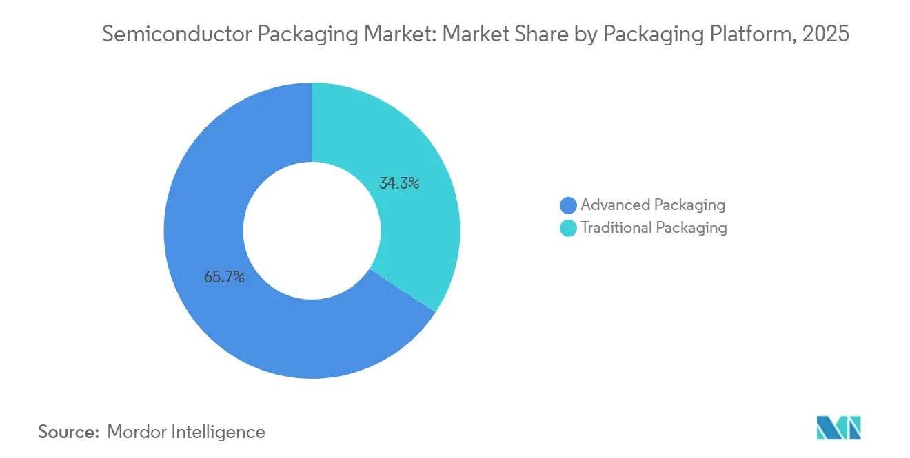
- By packaging platform, advanced packaging led with 65.71% revenue share in 2025 and is projected to expand at a 10.61% CAGR through 2031.
- By packaging material, organic substrates held 37.82% of the semiconductor packaging market share in 2025; ceramic packages are forecast to grow at an 11.67% CAGR through 2031.
- By wafer size, 300 mm wafers accounted for 59.17% of the volume in 2025; panel-level substrates are poised to grow at a 10.89% CAGR through 2031.
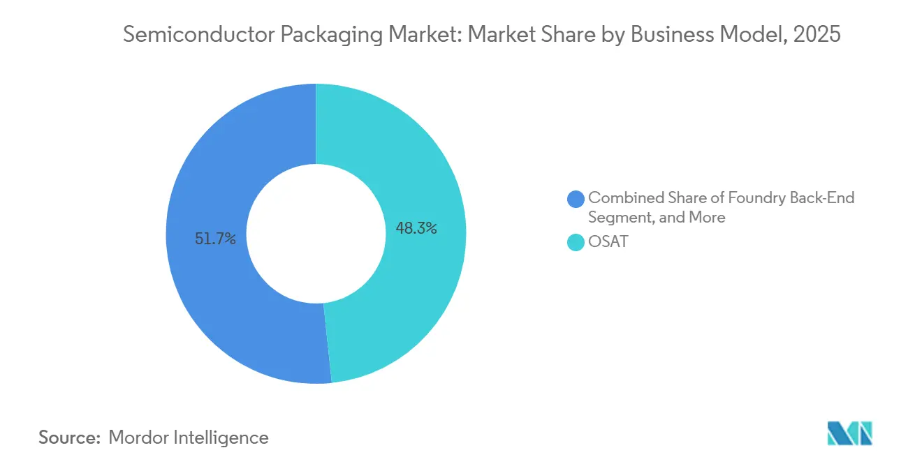
- By business model, outsourced assembly and test providers captured 48.33% revenue share in 2025, while foundry back-end operations are expected to register a 10.83% CAGR to 2031.
- By end-user industry, consumer electronics accounted for 43.49% of demand in 2025; automotive and mobility applications are anticipated to expand at an 11.43% CAGR through 2031.
- By geography, Asia-Pacific commanded a 66.89% share in 2025, whereas the Middle East is projected to post an 11.29% CAGR between 2026 and 2031.
Note: Market size and forecast figures in this report are generated using Mordor Intelligence’s proprietary estimation framework, updated with the latest available data and insights as of January 2026.
Global Semiconductor Packaging Market Trends and Insights
Drivers Impact Analysis*
| Driver | (~) % Impact on CAGR Forecast | Geographic Relevance | Impact Timeline |
|---|---|---|---|
| AI accelerator boom driving 2.5D/3D interposers | +2.3% | Global, concentrated in North America and Asia-Pacific | Medium term (2-4 years) |
| Electrified vehicle power packages | +1.8% | North America and Asia-Pacific core, spillover to Europe | Long term (≥ 4 years) |
| United States and EU CHIPS incentives | +1.5% | North America and Europe | Short term (≤ 2 years) |
| 5G RF-SiP demand in China and Korea | +1.2% | Asia-Pacific, primarily China and South Korea | Medium term (2-4 years) |
| Panel-level packaging for ultra-low-cost IoT | +1.0% | Global, early adoption in Asia-Pacific | Long term (≥ 4 years) |
| Chiplet architectures powering high-density interposers | +1.9% | Global, led by North America and Asia-Pacific | Medium term (2-4 years) |
| Source: Mordor Intelligence | |||
AI Accelerator Boom Driving 2.5D/3D Interposers
Hyperscale data-center operators now deploy clusters with more than 30,000 graphics processing units per site, each relying on high-yield interposers to connect logic dies to high-bandwidth memory stacks. Throughout 2025, TSMC reported CoWoS capacity utilization above 95%, prompting customers to secure slots through 2027.[1]“EU Chips Act Implementation Progress,” European Commission, ec.europa.eu At 2.5D geometries, average yield hovers near 75%, meaning one in four substrates is scrapped at a cost that can top USD 10,000 per defect. Intel’s Meteor Lake processors, shipped in 2024, demonstrated a 10-micron bump pitch, trimming package area by 40% but pushing thermal density toward 200 W/cm². Smaller fabless firms without long-term contracts face allocation risk as hyperscalers monopolize supply.
Electrified Vehicle Power Packages in the United States and Asia
Electric-vehicle inverters require power modules that survive junction temperatures above 200 °C and repeated 150 °C thermal cycles. Wolfspeed doubled automotive design wins for 800-volt architectures in fiscal 2025, with each inverter consuming up to 12 discrete modules.[2] Ceramic substrates from Kyocera and NGK Spark Plug exhibit thermal conductivities above 250 W/m·K but cost several times more than organic laminates. Domestic-content incentives in the United States prompted Infineon and ON Semiconductor to commit USD 2 billion in packaging investments across Texas and New York. China’s vertically integrated BYD and CATL likewise internalized module assembly to secure performance and margin.
United States and EU CHIPS Incentives Creating Local Back-End Fabs
By December 2025, the CHIPS and Science Act had issued USD 7.9 billion in grants and USD 25 billion in loan guarantees, with Amkor receiving USD 400 million to co-locate a USD 2-billion advanced-packaging plant beside TSMC’s Phoenix fab. In Europe, a EUR 3.3-billion (USD 3.5-billion) pool is underwriting a joint Infineon-GlobalFoundries project in Dresden.[3] Automation now cuts direct labor to below 15% of total cost, so proximity to wafer fabs and customers increasingly outweighs the cost advantage of low-wage locations in Southeast Asia.
Chiplet Architectures Powering High-Density Interposers
AMD’s MI300 accelerator integrates 13 chiplets on a single interposer, rendering 5.3 TB/s of memory bandwidth while trimming monolithic die cost by an estimated 35%. The Universal Chiplet Interconnect Express specification standardizes electrical, protocol, and mechanical interfaces, yet proprietary links from Intel, TSMC, and Samsung maintain latency advantages. Packaging lines must manage mixed bump pitches: 40 µm for logic, 55 µm for memory, and 100 µm for power, pushing per-line capital requirements beyond USD 500 million.
Restraints Impact Analysis*
| Restraint | (~) % Impact on CAGR Forecast | Geographic Relevance | Impact Timeline |
|---|---|---|---|
| ABF substrate supply crunch (Taiwan/Japan) | -1.2% | Global, most acute in Asia-Pacific | Short term (≤ 2 years) |
| Yield challenges in 3D TSV/hybrid bonding | -0.9% | Global, concentrated in advanced-packaging hubs | Medium term (2-4 years) |
| Export controls on advanced tools to China | -0.7% | Asia-Pacific, specifically China | Long term (≥ 4 years) |
| Thermal limits in fan-out WLP below 5 nm | -0.6% | Global, affecting high-performance computing and mobile | Medium term (2-4 years) |
| Source: Mordor Intelligence | |||
ABF Substrate Supply Crunch (Taiwan/Japan)
Ajinomoto Build-up Film substrates remained in short supply during 2025 because capacity expansions at Ibiden and Shinko Electric will not reach volume until mid-2026. Lead times for 12-layer substrates stretched to 38 weeks, forcing redesigns or performance compromises. One tier-1 cloud provider responded by investing USD 300 million in a Taiwanese joint venture to lock in supply.
Yield Challenges in 3D TSV/Hybrid Bonding
Through-silicon-via and hybrid bonding processes still lag conventional flip-chip yields by 15-25 percentage points. TSMC’s System-on-Integrated-Chips offering achieved 70% yield during early production, compared with 90% for mature CoWoS flows. A failed multi-die stack can waste USD 2,000–5,000 in silicon, and rework is often impossible. Intel’s Granite Rapids server roadmap slipped two quarters in 2024 due to similar issues.
*Our forecasts treat driver/restraint impacts as directional, not additive. The impact forecasts reflect baseline growth, mix effects, and variable interactions.
Segment Analysis
By Packaging Platform: Advanced Solutions Extend Leadership
Advanced formats accounted for 65.71% of the semiconductor packaging market share in 2025 and are set to grow at a 10.61% CAGR through 2031. Flip-chip remains dominant for high-pin-count devices as solder-bump pitch tightens to 80 µm. Fan-out wafer-level packaging delivers 20% savings in bill of materials for 5G RF front-ends, while system-in-package and package-on-package architectures optimize mobile footprints. The 2.5D/3D subsegment is the fastest climber, driven by AI accelerators that embed eight or more high-bandwidth memory stacks per interposer.
Panel-level packaging is emerging as a cost disruptor, expected to expand at a 10.89% CAGR through 2031. Rectangular 510 mm × 515 mm substrates yield 2.5 times as many dies as 300 mm wafers, lowering per-die cost by up to 40%. Yet new handling and inspection tools are required, pushing the learning curve to 24 months. Traditional wire-bond solutions preserve relevance in power management ICs, discrete transistors, and legacy automotive applications where cost and qualification inertia dominate.


By Packaging Material: Ceramic Uptick Counters Organic Dominance
Organic laminates held a 37.82% share in 2025, but Ajinomoto Build-up Film's supply constraints prompt design diversification. Leadframes, bonding wires, encapsulation resins, and solder balls collectively support price-sensitive devices. Copper wire adoption reached over 80% by 2025, saving USD 0.02–0.05 per unit compared with gold. Epoxy molding compounds now incorporate silicone variants to tolerate automotive temperatures above 150 °C.
Ceramic packages are forecast to grow at an 11.67% CAGR, driven by silicon-carbide and gallium-nitride power modules that require thermal conductivity above 200 W/m·K. Kyocera’s 2024 expansion increased aluminum nitride capacity by 25%. Die attach and thermal interface compounds have become critical as logic power density exceeds 100 W/cm². The semiconductor packaging market continues to scrutinize second-source options for ABF dielectric to avoid single-supplier risk.
By Wafer Size: Panel Economics Challenge the 300 mm Standard
The 300 mm format captured 59.17% of the 2025 volume thanks to mature tooling and widespread availability. Sizes below 200 mm persist in gallium arsenide RF and silicon carbide power devices, where substrate cost dictates the diameter. Panel-level packaging, classified here as above 450 mm, will grow at 10.89% as Nepes and ASE bring pilot lines online.
A single panel yields substantially more die than a 300 mm wafer because edge exclusion disappears. However, non-circular substrates oblige new lithography, handling, and metrology platforms. The installed base of USD 30 billion in 300 mm equipment creates inertia, so analysts expect panels to secure only 15-20% of low-cost devices by 2030, coexisting with wafer flows rather than replacing them.
By Business Model: Foundries Accelerate Backward Integration
Outsourced assembly and test providers controlled 48.33% of the semiconductor packaging market in 2025, yet foundry back-end services are on track for a 10.83% CAGR. TSMC, Samsung, and Intel are scaling InFO, I-Cube, X-Cube, and Foveros platforms to deliver turnkey solutions. Traditional OSATs respond with USD 3-billion capital plans for 2.5D and 3D lines, plus capacity-reservation programs that resemble long-term partnerships.
Integrated device manufacturers favor in-house packaging for proprietary products but admit escalating capital burden. Intel plans to outsource 30% of packaging volume by 2027, focusing internal lines on leading-edge stacks. Hyperscalers such as Amazon Web Services and Google Cloud now co-finance capacity, blurring the boundary between customer and supplier. The semiconductor packaging market landscape, therefore, spans pure-play OSATs, vertically integrated foundries, and hybrid consortia.

By End-User Industry: Automotive Surges Past Consumer Growth
Consumer electronics retained 43.49% of demand in 2025, yet smartphone unit shipments have plateaued at around 1.2 billion annually. Automotive and mobility solutions will grow at 11.43% through 2031, fueled by sensor fusion, lidar, and high-temperature power modules. Each electric-vehicle traction inverter consumes multiple silicon-carbide modules that require ceramic packages with thermal conductivity exceeding 250 W/m·K.
Computing and data-center devices command the highest average selling prices, with AI accelerators exceeding USD 30,000 per unit. Aerospace, medical, industrial, and energy segments rely on high-reliability, long-qualification packages rather than bleeding-edge performance. As these verticals stabilize demand, the semiconductor packaging market gains resilience against smartphone cyclicality.
Geography Analysis
Asia-Pacific controlled 66.89% of the semiconductor packaging market in 2025, anchored by Taiwan’s leadership in flip-chip and fan-out processing and China’s scale in mainstream assembly. Export controls enacted in October 2024 continue to limit mainland access to state-of-the-art tools, prompting domestic players to adopt hybrid-bonding workarounds that sacrifice yield for autonomy. South Korea’s Samsung and SK Hynix vertically integrate memory packaging, while Japan’s Shinko Electric and Ibiden dominate high-layer-count substrate fabrication.
North America’s share is rising as CHIPS Act incentives underwrite new lines in Arizona, New Mexico, Texas, and Ohio. Amkor’s USD 2-billion plant in Arizona and Intel’s packaging expansions bring advanced capability within the region, supporting defense and automotive security requirements. Europe remains smaller but is set to double capacity by 2030 through the EU Chips Act, with Germany’s Dresden cluster leading investment.
The Middle East exhibits the fastest regional CAGR at 11.29% as Saudi Arabia’s Public Investment Fund and the United Arab Emirates’ Mubadala channel oil revenues into semiconductor diversification. Greenfield assembly and test lines scheduled for 2027–2028 will target consumer and automotive modules before progressing to advanced interposers. South America and Africa maintain niche participation, focusing on wire-bond and leadframe services for localized industrial demand.

Competitive Landscape
The semiconductor packaging industry is moderately concentrated: the top 10 suppliers hold roughly 55% of global revenue. ASE Technology Holding, Amkor Technology, and JCET Group anchor the OSAT segment, whereas TSMC, Samsung, and Intel provide fully integrated wafer-to-package services. Strategy divergence is pronounced. Foundries leverage process control and customer lock-in, OSATs scale capacity across multiple regions, and hyperscalers increasingly co-invest to secure long-term output.
Technology differentiation now hinges on bump pitch, warpage control, and thermal management. Leaders in sub-10-micron hybrid bonding can claim an 80% yield, a threshold that laggards struggle to meet. Intellectual property intensity is rising: the United States Patent and Trademark Office recorded a 35% year-over-year increase in 2024 packaging-related filings, with Intel, TSMC, and Samsung each submitting more than 200 patents.
Substrate shortages and thermal constraints spawn collaboration across the value chain. Cloud providers fund ABF capacity to mitigate supply bottlenecks, and substrate vendors form joint ventures to diversify geographic exposure. Standardization under the Universal Chiplet Interconnect Express consortium, which grew to 120 members by late 2025, suggests that long-term competitive advantage will shift from proprietary interconnects to ecosystem integration.
Semiconductor Packaging Industry Leaders
Intel Corporation
Samsung Electronics Co., Ltd.
Taiwan Semiconductor Manufacturing Co. Ltd.
Micron Technology, Inc.
Texas Instruments Inc.
- *Disclaimer: Major Players sorted in no particular order

Recent Industry Developments
- December 2025: TSMC announced a USD 5 billion CoWoS capacity expansion in Taiwan, adding 50% output by mid-2027.
- November 2025: Samsung Electronics began volume production of X-Cube 3D packaging at Pyeongtaek, achieving sub-10-micron hybrid-bonding pitch.
- October 2025: Amkor Technology and TSMC signed a 10-year capacity reservation agreement covering Amkor’s Arizona facility.
- September 2025: ASE Technology Holding committed USD 500 million to panel-level fan-out capacity in Taiwan, targeting IoT devices.


Research Methodology Framework and Report Scope
Market Definitions and Key Coverage
Our study treats the semiconductor packaging market as all revenue earned from the sale of finished device packages, traditional lead-frame formats as well as advanced solutions such as fan-out wafer-level, flip-chip, 2.5D, and 3D stacked structures that protect, interconnect, and thermally manage integrated circuits.
Sales of ancillary equipment, raw materials, and front-end foundry services sit outside this boundary. Scope Exclusion: Packaging equipment, packaging materials, and outsourced test services remain out of scope unless they directly form part of the package value.
Segmentation Overview
- By Packaging Platform
- Advanced Packaging
- Flip-Chip
- Fan-Out WLP
- Fan-In WLP
- 2.5D / 3D IC
- Embedded-Die
- SiP / PoP
- Panel-Level Packaging
- Traditional Packaging
- Wire-Bond
- Leadframe
- QFN / QFP / SOP
- Advanced Packaging
- By Packaging Material
- Organic Substrates
- Leadframes
- Bonding Wires
- Encapsulation Resins
- Ceramic Packages
- Solder Balls and Bumps
- Die-Attach and TIMs
- By Wafer Size
- Below 200 mm
- 300 mm
- Above 450 mm / Panel
- By Business Model
- OSAT
- Foundry Back-End
- IDM In-house
- By End-user Industry
- Consumer Electronics
- Smartphones and Wearables
- PCs, Tablets, and Consumer Devices
- Computing and Data Center
- Automotive and Mobility
- Communications and Telecom
- Aerospace and Defense
- Medical and Healthcare Devices
- Industrial and Energy (LED / Power)
- Consumer Electronics
- By Geography
- North America
- United States
- Canada
- Mexico
- Europe
- Germany
- United Kingdom
- France
- Rest of Europe
- Asia-Pacific
- China
- Japan
- India
- South Korea
- Taiwan
- Rest of Asia-Pacific
- Rest of the World
- North America
Detailed Research Methodology and Data Validation
Primary Research
Mordor analysts interview OSAT executives, foundry back-end managers, substrate suppliers, and purchasing leads across Asia, North America, and Europe. Conversations validate average selling prices, yield drifts, and the pace at which automotive accounts convert from wire-bond to flip-chip. Follow-up surveys with packaging design engineers clarify the expected share of 2.5D/3D architectures in AI accelerators during the forecast window.
Desk Research
Publicly available tier-one sources form our starting grid. Data from organizations such as SEMI, WSTS, and national customs portals outline production, trade, and capital-spending flows, while JEITA and SIA bulletins reveal demand signals in downstream electronics. Company 10-Ks, investor decks, and patent registries add contextual color on technology migration toward chiplets and hybrid bonding. To fill regional gaps, we access paid repositories (D&B Hoovers for corporate revenue splits and Dow Jones Factiva for deal news). The list above is illustrative, and many additional sources guide the desk phase.
Government incentives, for example, the U.S. CHIPS Act award list, and trade association shipment tallies help us capture fingerprints such as ABF substrate price spikes, fan-out line utilization, and panel-level pilot volumes, providing real-time anchors for the model.
Market-Sizing & Forecasting
A top-down reconstruction starts with global semiconductor sales, filters through packageable die share, and applies penetration factors for each packaging platform; selective bottom-up checks, sampled OSAT revenue roll-ups and ASP × volume calculations, tune the totals. Key variables include advanced-node wafer starts, substrate capacity additions, fan-out panel shipments, average layer count in HBM stacks, automotive semiconductor content per vehicle, and prevailing ASP deltas between traditional and advanced formats. Multivariate regression projecting these drivers underpins the 2025-2030 outlook. Gap areas, such as captive in-house packaging at IDMs, are bridged with calibrated ratios from expert interviews before final reconciliation.
Data Validation & Update Cycle
Draft numbers pass variance screens against trade, pricing, and company guidance benchmarks, then move to a two-level analyst review. Our models refresh every twelve months, with interim revisits if material events, like a substrate fab fire or a sudden export control, shift baseline assumptions.
Why Mordor's Semiconductor Packaging Baseline Proves Dependable
Published estimates often diverge because firms pick different coverage slices, currency bases, or refresh cadences. Users want clarity on why totals vary and which figure deserves confidence.
Key gap drivers arise when others bundle packaging materials, exclude advanced fan-out lines, or convert currencies at spot rather than full-year averages, thereby understating 2025 inflammation effects. Some providers freeze scenarios for three-plus years, while Mordor's annual refresh captures new CHIPS-funded capacity and the 19% surge in AI-driven 2.5D demand.
Benchmark comparison
| Market Size | Anonymized source | Primary gap driver |
|---|---|---|
| USD 49.88 B (2025) | Mordor Intelligence | |
| USD 43.95 B (2024) | Global Consultancy A | Excludes advanced fan-out and 2.5D volumes; uses spot FX |
| USD 55.02 B (2025) | Regional Consultancy B | Bundles packaging materials and test services; limited primary validation |
In sum, Mordor Intelligence delivers a balanced, transparent baseline rooted in clearly defined scope, annually refreshed variables, and dual validation steps, giving decision-makers a figure they can trace and replicate with confidence.


Key Questions Answered in the Report
What is the projected value of the semiconductor packaging market in 2031?
The semiconductor packaging market is forecast to reach USD 156.41 billion by 2031, growing at a 8.70% CAGR.
Which segment currently leads platform adoption?
Advanced packaging leads with 65.71% share in 2025 and continues to expand faster than traditional wire-bond options.
Why are ceramic packages gaining share?
Electric-vehicle inverters and other high-temperature modules need thermal conductivity above 200 W/m·K, which ceramic substrates deliver.
How will CHIPS Act funding affect regional capacity?
United States grants and loan guarantees are underwriting new lines in Arizona, New Mexico, Texas, and Ohio, boosting North American advanced-packaging capacity by more than 20% by 2028.
What factors limit panel-level packaging adoption?
Non-circular panels require new lithography and inspection tools, and yield learning curves can extend 24 months, restraining rapid migration from established 300 mm wafer lines.
Page last updated on:


