Thin Layer Deposition Market Size and Share
Market Overview
| Study Period | 2020 - 2031 |
|---|---|
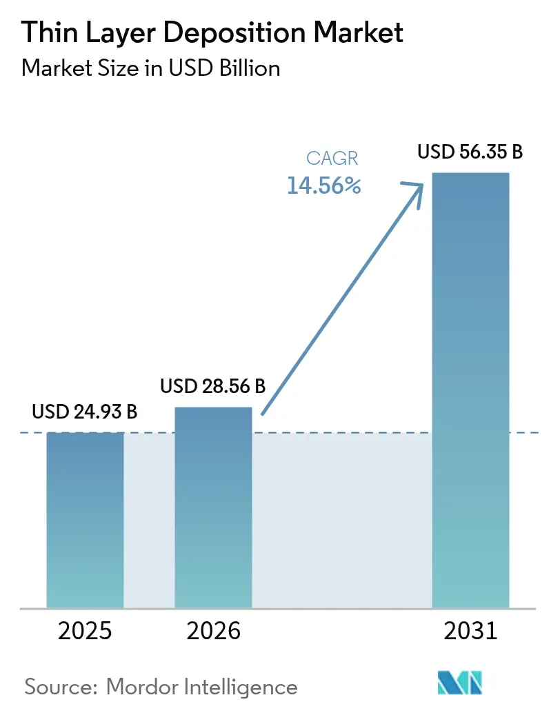
| Market Size (2026) | USD 28.56 Billion |
| Market Size (2031) | USD 56.35 Billion |
| Growth Rate (2026 - 2031) | 14.56% CAGR |
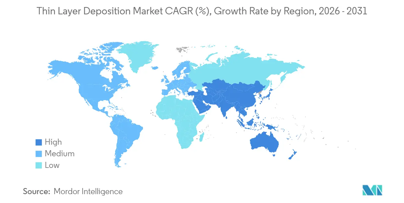
| Fastest Growing Market | Asia Pacific |
| Largest Market | Asia Pacific |
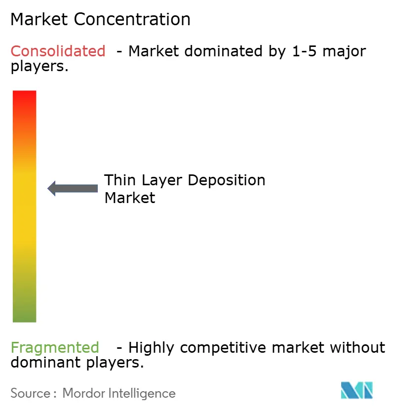
| Market Concentration | Medium |
Major Players *Disclaimer: Major Players sorted in no particular order Image © Mordor Intelligence. Reuse requires attribution under CC BY 4.0. | |
Thin Layer Deposition Market Analysis by Mordor Intelligence
The thin layer deposition market size was valued at USD 24.93 billion in 2025 and estimated to grow from USD 28.56 billion in 2026 to reach USD 56.35 billion by 2031, at a CAGR of 14.56% during the forecast period (2026-2031). Growth stems from structural shifts in semiconductor scaling, perovskite tandem photovoltaics, and medical-grade surface engineering. Foundries rely on atomic layer deposition for sub-5-nanometer gate stacks, while solar manufacturers adopt roll-to-roll physical vapor deposition to reduce the cost per watt. Government CHIPS-style incentives channel capital toward domestic equipment plants, and AI-driven predictive maintenance reduces tool downtime, thereby increasing overall equipment effectiveness. Material diversification into nitrides, carbides, and 2D compounds opens up incremental revenue streams for specialty chemical suppliers and toolmakers. At the same time, helium scarcity, Scope-3 carbon rules, and talent shortages temper the growth outlook, nudging suppliers to develop closed-loop gas recovery and low-power reactor designs.
Key Report Takeaways
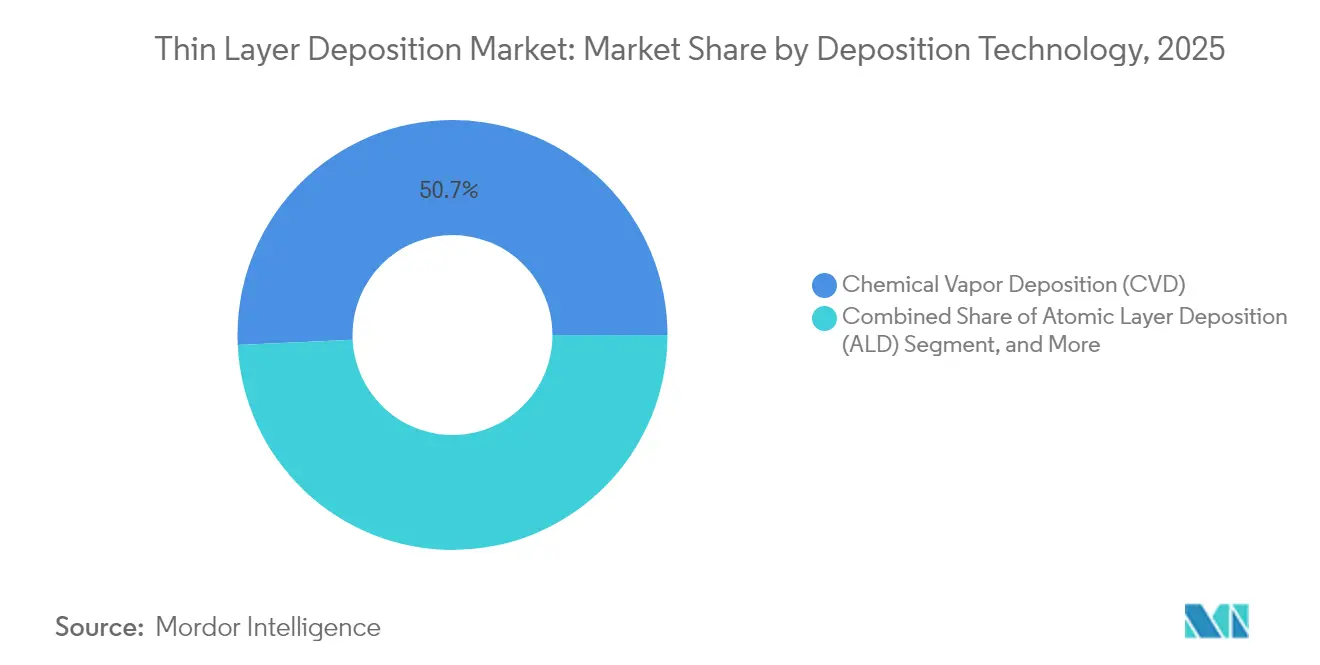
- By deposition technology, chemical vapor deposition accounted for 50.74% of the thin layer deposition market size in 2025, while atomic layer deposition is advancing at a 17.18% CAGR to 2031.
- By equipment type, batch systems accounted for 56.05% of the thin layer deposition market size in 2025, and roll-to-roll plus spatial systems are projected to expand at a 16.36% CAGR through 2031.
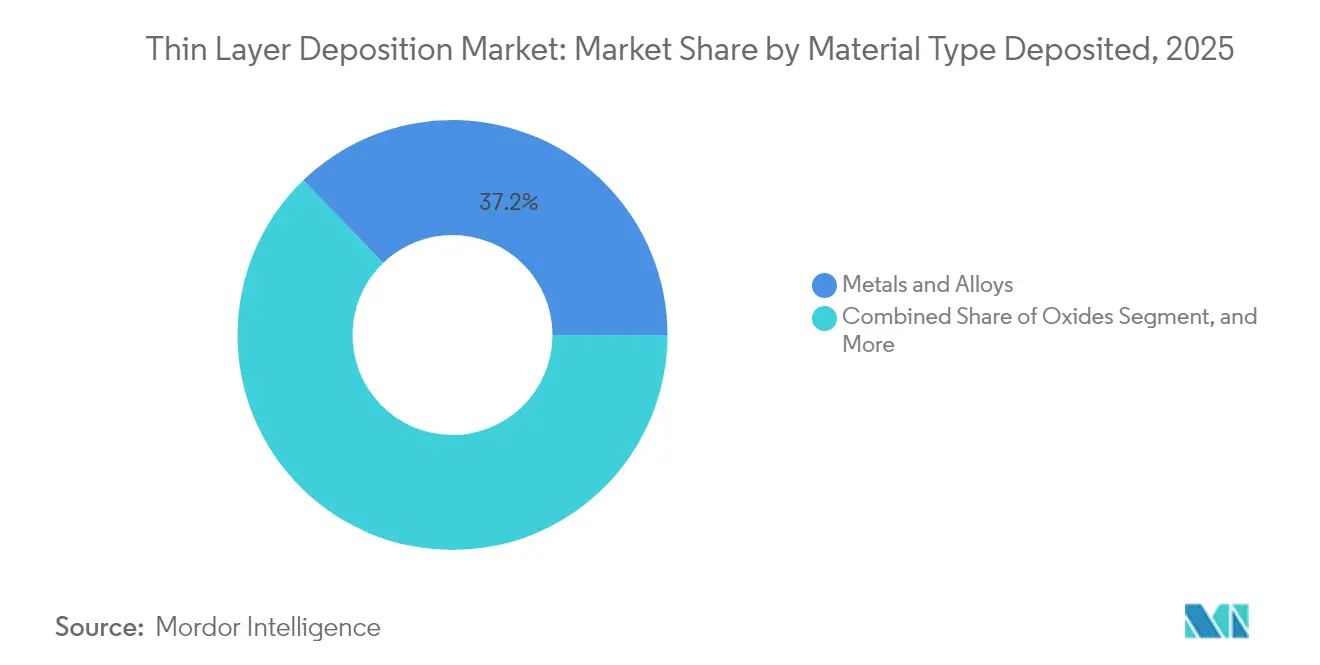
- By material type deposited, metals and alloys accounted for 37.22% of the thin layer deposition market size in 2025, and nitrides and carbides are projected to expand at a 17.01% CAGR through 2031.
- By end-use industry, semiconductors and micro-electronics captured 41.35% of the thin layer deposition market size in 2025, whereas photovoltaics and energy storage is forecast to post an 17.74% CAGR until 2031.
- By geography, the Asia Pacific commanded 44.78% of the thin layer deposition market size in 2025, and is poised to grow at a 16.92% CAGR over the next five years.
Note: Market size and forecast figures in this report are generated using Mordor Intelligence’s proprietary estimation framework, updated with the latest available data and insights as of 2026.
Global Thin Layer Deposition Market Trends and Insights
Drivers Impact Analysis*
| Driver | (~) % Impact on CAGR Forecast | Geographic Relevance | Impact Timeline |
|---|---|---|---|
| Chiplet and 3D-IC architectures intensify the need for ultra-conformal interconnect films | +3.2% | Global with hubs in Taiwan, South Korea, United States | Medium term (2-4 years) |
| Rapid scale-up of perovskite tandem solar cell manufacturing | +2.8% | Asia Pacific core, spillover to Europe and Middle East | Medium term (2-4 years) |
| Spatial ALD and roll-to-roll PVD breakthroughs slashing cost per nanometer | +2.5% | Global, early adoption in China, Germany, United States | Short term (≤ 2 years) |
| Government CHIPS-like incentives boosting domestic deposition tool CAPEX | +2.1% | United States, European Union, India, Japan | Long term (≥ 4 years) |
| AI-powered predictive maintenance reducing deposition tool downtime | +1.6% | Global, led by advanced fabs in Taiwan, South Korea, United States | Short term (≤ 2 years) |
| Emergence of biodegradable implant coatings in med-tech | +0.9% | North America and Europe | Long term (≥ 4 years) |
| Source: Mordor Intelligence | |||
Chiplet And 3D-IC Architectures Intensify The Need For Ultra-Conformal Interconnect Films
Heterogeneous integration is changing interconnect design, demanding barrier and seed layers that cover high-aspect-ratio vias without voids. Taiwan Semiconductor Manufacturing Company’s CoWoS-S stacks logic with high-bandwidth memory using 20:1 aspect-ratio through-silicon vias that require titanium nitride deposited by atomic layer deposition for copper diffusion control. Intel’s 2024 Foveros Direct technology reduced bump pitch to 25 μm, forcing a shift to cobalt seed layers with 95% step coverage that chemical vapor deposition struggles to achieve. Samsung Foundry aims for 2 μm line-and-space redistribution by 2027, which will rely on plasma-enhanced atomic layer deposition of ruthenium liners. Tool vendors saw orders surge; Applied Materials reported 38% year-over-year growth in advanced-packaging deposition tools in fiscal 2024.[1]Applied Materials Inc., “Form 10-K FY 2024,” sec.gov Industry consortia are pushing new precursors, such as cyclopentadienyl-based ruthenium, to enable sub-300 °C processing compatible with organic interposers.
Rapid Scale-Up of Perovskite Tandem Solar Cell Manufacturing
Perovskite-silicon tandems surpassed the 33% efficiency mark in 2024, sparking a surge in the development of pilot lines. Oxford Photovoltaics commenced 200 MW production in Brandenburg, utilizing slot-die perovskite layers in combination with PECVD tin oxide electron transport films. Longi has partnered with Meyer Burger to integrate perovskites into TOPCon modules, aiming for 30% efficiency by 2026. The U.S. Department of Energy has granted USD 40 million to spatial atomic layer deposition projects, aiming for 10× throughput gains in passivation layers. Venture capital is flowing: Swift Solar raised USD 27 million to commercialize lightweight tandem panels that rely on roll-to-roll sputtered transparent conductors. The International Energy Agency forecasts 50 GW of tandem capacity by 2030, provided that deposition tools maintain uptime above 90% and material utilization exceeds 70%.
Spatial ALD And Roll-To-Roll PVD Breakthroughs Slashing Cost Per Nanometer
Spatial atomic layer deposition eliminates pump-down cycles by moving substrates through isolated precursor zones, achieving 300 mm wafer throughput of nearly 1,000 units per hour. Beneq’s 2024 demo hit 5 nm min⁻¹ Al₂O₃ on flexible polyimide with around 2% uniformity across 600 mm webs. Veeco’s Picosun roll-to-roll system coated lithium-ion separators at 10 m/min⁻, cutting the cost per square meter from USD 0.50 to USD 0.08. Applied Materials’ Olympia platform integrates spatial atomic layer deposition and physical vapor deposition within a single cluster, reducing cobalt liner and copper seed times by 40%. On the sputtering front, Von Ardenne logged 100 nm s⁻¹ ITO rates on 1.5 m glass, halving capex for display backplanes. NREL demonstrated that roll-to-roll CdTe modules could achieve 18% efficiency at sub-USD 0.20 W⁻¹ costs, reinforcing the thin film’s cost edge.
Government CHIPS-Like Incentives Boosting Domestic Deposition Tool CAPEX
The U.S. CHIPS and Science Act earmarked USD 39 billion in grants and USD 75 billion in loan guarantees, triggering a home-grown equipment supply push. Intel’s Arizona build secured USD 8.5 billion and includes 150 deposition tools slated for 18-Å nodes by 2026. Europe’s EUR 43 billion Chips Act funds fabs in Germany, where Infineon and TSMC Dresden expansions will install 200 reactors. India accounts for up to 50% of fab capex; Micron’s Gujarat assembly plant will utilize 80 PVD tools. Japan pledged JPY 2 trillion to Rapidus for 2nm logic, prompting tool orders to be directed to Tokyo Electron. China’s “Big Fund” phase III added USD 47.5 billion to localize CVD and ALD hardware at AMEC and NAURA.
Restraints Impact Analysis*
| Restraint | (~) % Impact on CAGR Forecast | Geographic Relevance | Impact Timeline |
|---|---|---|---|
| Helium and high-purity precursor supply crunch inflates OPEX | -2.4% | Global, acute in United States, Europe, Japan | Short term (≤ 2 years) |
| Escalating Scope-3 carbon-reporting mandates penalize vacuum processes | -1.8% | North America and Europe | Medium term (2-4 years) |
| Skilled vacuum-process talent shortage lengthens fab ramps | -1.3% | United States, Germany, Japan, India | Long term (≥ 4 years) |
| Competition from additive manufacturing of functional layers | -0.7% | Niche uses in North America, Europe, Asia Pacific | Medium term (2-4 years) |
| Source: Mordor Intelligence | |||
Helium And High-Purity Precursor Supply Crunch Inflates OPEX
The U.S. Federal Helium Reserve depletion drove spot prices from USD 8 m⁻³ in 2023 to USD 16 m⁻³ by mid-2024.[2]U.S. Bureau of Land Management, “Federal Helium Reserve Status,” blm.gov A 300 mm fab consumes 15 million m³ annually, and Lam Research disclosed USD 12 million extra helium costs in fiscal 2024. Closed-loop recovery systems recapture 95% of process gas but cost USD 3 million per installation. High-k precursors face similar strain; hafnium tetrachloride capacity is restricted to three makers, stretching lead times from 8 to 20 weeks. China’s August 2024 export controls on zirconium compounds further tightened the supply, prompting fabs to enter into dual-source agreements that increase unit costs by 18%.
Escalating Scope-3 Carbon-Reporting Mandates Penalize Vacuum Processes
The U.S. SEC now mandates Scope-3 disclosure from fiscal 2026, and the EU’s CSRD already applies to firms with over 250 employees.[3]U.S. Securities and Exchange Commission, “Climate Disclosure Rules,” sec.gov An atomic layer deposition reactor draws 40-60 kW in deposition mode, making vacuum tools significant emitters. ASM International recorded 18 tCO₂e per Pulsar tool per year when powered by EU-average grids. Customers respond by situating fabs near renewable energy clusters and by adopting Applied Materials’ Centura variant, which reduces idle power by 30% through adaptive throttling. Carbon pricing above EUR 80 t⁻¹ in the EU adds further pressure.
*Our forecasts treat driver/restraint impacts as directional, not additive. The impact forecasts reflect baseline growth, mix effects, and variable interactions.
Segment Analysis
By Deposition Technology: Atomic Layer Deposition Gains As Logic Nodes Shrink
Chemical vapor deposition held a 50.74% market share in the thin layer deposition market in 2025, reflecting its versatility in depositing dielectrics, polysilicon, and tungsten at high rates. Atomic layer deposition is forecast to grow at a 17.18% CAGR, driven by the need for sub-3 nm transistor gates, which require angstrom-scale thickness control. The thin layer deposition market size allocated to ALD reached USD 9.2 billion in 2025 and is expected to double by 2031. Physical vapor deposition remains entrenched for aluminum interconnects at mature nodes; however, hybrid flows, such as Lam Research’s SABRE 3D, merge ionized PVD with ALD barriers to reduce interface resistance by 25%. The emerging molecular layer deposition of polymers broadens the functional options for flexible electronics, adding a nascent but fast-growing revenue stream.
Logic foundries moving to gate-all-around nanosheets employ up to 15 ALD steps, versus eight in the prior generation. Intel’s 18A node epitomizes this leap with hafnium oxide and titanium nitride stacks wrapped around channels with 5:1 aspect ratios. CVD maintains dominance in shallow trench isolation and inter-layer dielectric gap-fill because 100 nm min⁻¹ rates keep wafer costs down. As aspect ratios increase, suppliers are advancing high-density plasma CVD and high-reflow liners to delay switchover points. Selective deposition is an active frontier: Tokyo Electron’s Tactras Vigus tool combines ALE and ALD with in-situ metrology, achieving ±0.5 nm self-aligned contacts that could eliminate lithography steps in the next logic cycle.


By Equipment Type: Spatial Systems Disrupt Batch Dominance
Batch furnaces delivered 56.05% of 2025 revenue, prized for their low cost per wafer in commodity logic, solar, and optical coatings. However, roll-to-roll and spatial tools registered a 16.36% CAGR, reflecting a pivot toward flexible OLED displays, battery separators, and bifacial solar modules that need web-based continuous processing. Single-wafer clusters remain indispensable in advanced logic and 3D NAND, where vacuum-integrated chambers ensure particle control. The thin layer deposition market size for spatial ALD equipment was USD 2.8 billion in 2025 and is expected to reach USD 6 billion by 2031 as throughput concerns ease.
Beneq’s spatial ALD uptime moved past 85% in 2024, removing a historical barrier to mass adoption. Applied Materials’ Olympia integrates spatial ALD and PVD modules in a shared transfer system, achieving 1,200 wafers per hour for TOPCon passivation, a 15× productivity increase over batch reactors. Roll-to-roll magnetron sputtering at Von Ardenne coats indium zinc oxide on polyimide at a rate of 20 m min⁻¹, enabling foldable phones with a bend radius of 3 mm. Canon Anelva’s ENAS platform integrates machine learning into sputter power control, reducing thickness variation to around 1.5% on 300 mm wafers, thereby easing process windows for sub-10 nm copper interconnects.
By Material Type Deposited: Nitrides And Carbides Surge In Power Electronics
Metals and alloys accounted for 37.22% of the 2025 volume, led by copper, aluminum, and titanium. Nitrides and carbides posted a 17.01% CAGR owing to titanium nitride barriers, aluminum nitride heat spreaders, and silicon carbide interfaces. The thin layer deposition market size for nitrides alone exceeded USD 6 billion in 2025. Oxides remain indispensable for dielectrics and passivation, while 2D compounds, such as molybdenum disulfide and hexagonal boron nitride, gain early traction in neuromorphic and quantum devices.
Applied Materials’ Endura Volta deposited titanium nitride with 90% step coverage in 2:1 trenches, allowing TSMC’s 3 nm node to gain 15% speed over tantalum nitride baselines. Aluminum nitride’s 285 W m⁻¹ K⁻¹ thermal conductivity boosts GaN radio-frequency amplifiers, and Aixtron’s AIX G5 WW C reactor achieved ±3% film uniformity on 200 mm silicon carbide wafers. Research at Osaka University showed that nitric oxide-annealed oxides on silicon carbide trimmed interface traps are below 1×10¹¹ cm⁻² eV⁻¹, a critical metric for electric vehicle traction inverters.
By End-Use Industry: Photovoltaics Accelerate Past Semiconductor Growth
Semiconductors absorbed 41.35% of the 2025 spend but will grow at a slower rate than photovoltaics, which posts an 17.74% CAGR on the back of TOPCon and heterojunction architectures that require ALD aluminum oxide passivation. Photovoltaic demand pushed the thin layer deposition market size for solar applications to USD 5.7 billion in 2025. Medical devices, optics, and industrial tooling round out demand with specialty coatings that command higher margins per wafer equivalent.
Longi’s TOPCon modules achieved 25.5% efficiency using ALD rear passivation, increasing the energy yield per area by 1.5 percentage points. LG Energy Solution coats 1.2 m-wide polyethylene separators at a rate of 5 m/min⁻, covering 500 MWh of battery output annually. In med-tech, 200 nm hydroxyapatite layers extended the integrity of magnesium stents from 3 to 12 months, opening a new premium tool segment. OLED displays require ALD encapsulation, delivering water vapor transmission below 1 × 10⁻⁶ g m⁻² day⁻¹, as adopted by Samsung Display’s QD-OLED TVs.
Geography Analysis
The Asia Pacific region controlled 44.78% of 2025 revenue, driven by fabrication expansions at TSMC, Samsung, and multiple Chinese foundries. Capital spending in the region exceeded USD 36 billion, with TSMC alone accounting for a significant portion, 25% of which was earmarked for deposition equipment. China increased its equipment self-sufficiency to 28% in 2024, as AMEC tools were integrated into SMIC’s 14 nm lines. South Korean subsidies of KRW 20 trillion supported SK Hynix’s HBM ramps that ordered 120 ALD reactors. Japan’s Rapidus alliance purchased 30 tools for gate-to-gate R&D, leveraging expertise from IBM and IMEC.
North America is rebounding under the CHIPS Act. Intel and TSMC Phoenix will install more than 300 reactors by 2026, while Micron’s New York DRAM fab plans to use 80 ALD tools for capacitor dielectrics. Applied Materials broke ground on a USD 4 billion factory in Montana to serve this surge, adding 200,000 square feet of cleanrooms. Europe focuses on power and compound semiconductors; Infineon’s Dresden fab and TSMC European JV add 60 PVD and CVD tools for silicon carbide and copper interconnects. Middle East solar mega-projects, such as Saudi Arabia’s 20 GW tender, order large-area sputter lines from Von Ardenne and Singulus, thereby extending the regional share. South America and Africa remain nascent, but they benefit indirectly from commodity solar imports that rely on Asian manufacturing capacity. Regional research institutes explore roll-to-roll ALD for flexible sensors, building local know-how that could translate into modest equipment sales post-2030. Collectively, these emerging regions represent under 5% of current revenue, yet they provide a long tail of opportunity once cost curves fall.

Competitive Landscape
Market concentration is moderate, with the top five suppliers accounting for 65% of the 2024 revenue. Applied Materials, Lam Research, and Tokyo Electron dominate the single-wafer cluster market, while ASM International and Veeco focus on the ALD and MOCVD niches. Beneq, Picosun, and Kurt J. Lesker thrive in spatial ALD and R&D-scale systems. Competitive intensity rises as customers demand integrated deposition-etch-metrology platforms that shrink footprint and support real-time control. Lam Research’s Striker selective tungsten fill exemplifies horizontal expansion beyond etch.
Throughput, uniformity, and precursor efficiency remain the key differentiators. Applied Materials’ Olympia achieved 98% trimethylaluminum utilization, cutting TOPCon cost per wafer to USD 0.12. Lam Research’s AI suite reduced downtime to 3%, and Tokyo Electron filed 87 ALD patents in 2024, with a focus on selective area flows. Smaller rivals disrupt niches: CVD Equipment’s roll-to-roll graphene system won a European battery contract at 60% lower capex than batch solutions. Patent races spill into precursors, where ASM International secured rights to high-vapor-pressure plasma ALD chemistries, eliminating the need for heated lines.
Supply chain localization reshapes competition. AMEC received USD 180 million orders from SMIC for Prismo HiT3 etch-deposition clusters after U.S. export controls tightened. Beneq’s JV with Longi will build 100 spatial ALD tools annually in Xi’an, cutting lead times by 50%. Oerlikon Balzers has added ten Rapid Coating Units in Germany to address tool coatings, demonstrating that industrial PVD continues to grow under the umbrella of energy transition manufacturing.
Thin Layer Deposition Industry Leaders
Applied Materials Inc.
Lam Research Corporation
Tokyo Electron Limited
ASM International NV
Veeco Instruments Inc.
- *Disclaimer: Major Players sorted in no particular order

Recent Industry Developments
- October 2025: Applied Materials committed USD 4 billion to expand deposition tool manufacturing in Kalispell, Montana
- September 2025: Lam Research won a USD 1.2 billion contract from Samsung Foundry for 1.4 nm cobalt and ruthenium deposition tools
- August 2025: Tokyo Electron introduced Tactras Vigus, merging ALD, ALE, and metrology in one cluster, with 25 units ordered by TSMC
- July 2025: ASM International acquired Forge Nano for USD 320 million to access spatial ALD reactors for battery cathodes


Global Thin Layer Deposition Market Report Scope
The Thin Layer Deposition Market Report is Segmented by Deposition Technology (Physical Vapor Deposition, Chemical Vapor Deposition, Atomic Layer Deposition, Hybrid and Emerging Techniques), Equipment Type (Batch Systems, Single-Wafer Cluster Tools, Roll-To-Roll and Spatial Systems, In-Line Production Lines), Material Type Deposited (Metals and Alloys, Oxides, Nitrides and Carbides, Compound and 2-D Materials), End-Use Industry (Semiconductors and Micro-Electronics, Photovoltaics and Energy Storage, Medical Devices and Healthcare, Optics and Displays, Tools and Industrial Components), and Geography (North America, South America, Europe, Asia Pacific, Middle East and Africa). The Market Forecasts are Provided in Terms of Value in USD.
| Physical Vapor Deposition (PVD) |
| Chemical Vapor Deposition (CVD) |
| Atomic Layer Deposition (ALD) |
| Hybrid / Emerging Techniques |
| Batch Systems |
| Single-wafer Cluster Tools |
| Roll-to-Roll / Spatial Systems |
| In-line Production Lines |
| Metals and Alloys |
| Oxides |
| Nitrides and Carbides |
| Compound / 2-D Materials |
| Semiconductors and Micro-electronics |
| Photovoltaics and Energy Storage |
| Medical Devices and Healthcare |
| Optics and Displays |
| Tools and Industrial Components |
| North America | United States | |
| Canada | ||
| Mexico | ||
| South America | Brazil | |
| Argentina | ||
| Rest of South America | ||
| Europe | Germany | |
| United Kingdom | ||
| France | ||
| Italy | ||
| Spain | ||
| Russia | ||
| Rest of Europe | ||
| Asia Pacific | China | |
| Japan | ||
| India | ||
| South Korea | ||
| Australia | ||
| Rest of Asia Pacific | ||
| Middle East and Africa | Middle East | Saudi Arabia |
| United Arab Emirates | ||
| Turkey | ||
| Rest of Middle East | ||
| Africa | South Africa | |
| Nigeria | ||
| Egypt | ||
| Rest of Africa | ||
| By Deposition Technology | Physical Vapor Deposition (PVD) | ||
| Chemical Vapor Deposition (CVD) | |||
| Atomic Layer Deposition (ALD) | |||
| Hybrid / Emerging Techniques | |||
| By Equipment Type | Batch Systems | ||
| Single-wafer Cluster Tools | |||
| Roll-to-Roll / Spatial Systems | |||
| In-line Production Lines | |||
| By Material Type Deposited | Metals and Alloys | ||
| Oxides | |||
| Nitrides and Carbides | |||
| Compound / 2-D Materials | |||
| By End-Use Industry | Semiconductors and Micro-electronics | ||
| Photovoltaics and Energy Storage | |||
| Medical Devices and Healthcare | |||
| Optics and Displays | |||
| Tools and Industrial Components | |||
| By Geography | North America | United States | |
| Canada | |||
| Mexico | |||
| South America | Brazil | ||
| Argentina | |||
| Rest of South America | |||
| Europe | Germany | ||
| United Kingdom | |||
| France | |||
| Italy | |||
| Spain | |||
| Russia | |||
| Rest of Europe | |||
| Asia Pacific | China | ||
| Japan | |||
| India | |||
| South Korea | |||
| Australia | |||
| Rest of Asia Pacific | |||
| Middle East and Africa | Middle East | Saudi Arabia | |
| United Arab Emirates | |||
| Turkey | |||
| Rest of Middle East | |||
| Africa | South Africa | ||
| Nigeria | |||
| Egypt | |||
| Rest of Africa | |||


Key Questions Answered in the Report
What is the expected value of the thin layer deposition market by 2031?
The market is projected to reach USD 56.35 billion by 2031, reflecting a 14.56% CAGR
Which deposition technology is growing the fastest?
Atomic layer deposition is advancing at a 17.18% CAGR due to its role in sub-3 nm transistor and capacitor fabrication
Why is Asia Pacific the largest region for thin layer deposition?
Concentrated investments by TSMC, Samsung, and Chinese foundries drive 44.78% regional share and a 16.92% growth rate.
How are CHIPS-style incentives affecting equipment demand?
Subsidies in the United States, EU, India, and Japan accelerate domestic tool purchases, adding hundreds of CVD and ALD reactors to new fabs.
What materials segment shows the highest growth?
Nitrides and carbides post a 17.01% CAGR, propelled by titanium nitride barriers and aluminum nitride heat spreaders for power electronics.
How are suppliers mitigating helium shortages?
Fabs install closed-loop helium recovery, while tool makers redesign reactors for lower flow rates, limiting operating expense spikes.
Page last updated on:


