India Semiconductor Silicon Wafer Market Size and Share
Market Overview
| Study Period | 2020 - 2031 |
|---|---|
| Forecast Data Period | 2026 - 2031 |
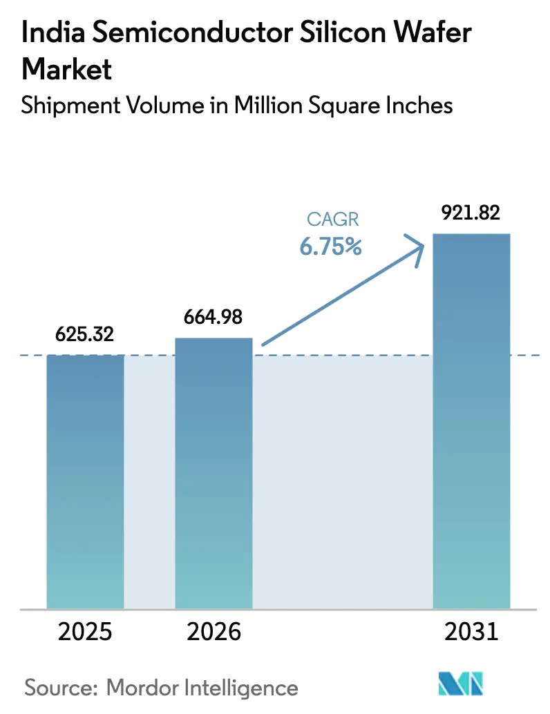
| Base Year Market Size (2025) | 625.32 Million Square Inches |
| Market Volume (2026) | 664.98 Million Square Inches |
| Market Volume (2031) | 921.82 Million Square Inches |
| Growth Rate (2026 - 2031) | 6.75% CAGR |
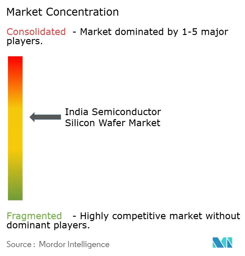
| Market Concentration | Medium |
Major Players *Disclaimer: Major Players sorted in no particular order Image © Mordor Intelligence. Reuse requires attribution under CC BY 4.0. | |
India Semiconductor Silicon Wafer Market Analysis by Mordor Intelligence
The India semiconductor silicon wafer market size is projected to be 625.32 million square inches in 2025, 664.98 million square inches in 2026 and reach 921.82 million square inches by 2031, growing at a CAGR of 6.75% from 2026 to 2031. A rapid pivot from import-dependence toward domestic fabrication is underway, underpinned by the India Semiconductor Mission’s multi-year capital subsidies. New 300 mm capacity coming online in Gujarat and Uttar Pradesh signals that the country is positioning itself as a high-volume, mature-node manufacturing hub. Domestic demand is rising in tandem: FY25 electronics output touched INR 11.3 lakh crore (USD 135 billion), while smartphone and electric-vehicle programs keep end-market pull robust. The India semiconductor silicon wafer market is also benefiting from the entry of global players that view India as a risk-diversification node in their Asia-Pacific footprint. Even so, execution remains contingent on power reliability, ultra-pure water availability and timely tool deliveries, all of which require tight government-industry coordination.
Key Report Takeaways
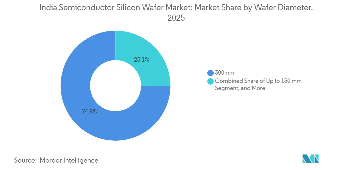
- By wafer diameter, the 300 mm segment led with 74.88% of the India semiconductor silicon wafer market share in 2025 and is advancing at a 7.11% CAGR through 2031.
- By device type, logic devices accounted for 35.61% of volume in 2025 and are expanding at a 7.36% CAGR between 2026-2031.
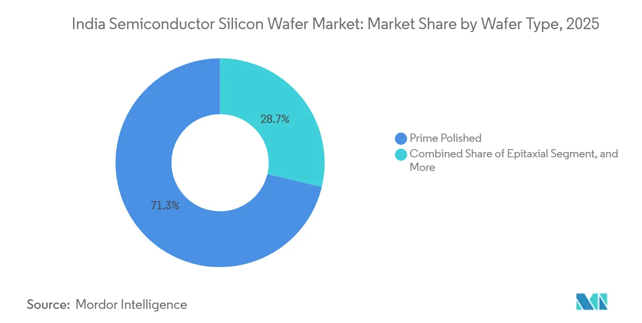
- By wafer type, prime polished substrates captured 71.28% share of the India semiconductor silicon wafer market size in 2025, while silicon-on-insulator wafers post the fastest 6.28% CAGR to 2031.
- By end-user, consumer electronics dominated with 39.63% share of wafer demand in 2025; the automotive segment records the highest 6.18% CAGR through 2031.
Note: Market size and forecast figures in this report are generated using Mordor Intelligence’s proprietary estimation framework, updated with the latest available data and insights as of January 2026.
National developments in India connect differently with activity unfolding across other parts of the world. In the global semiconductor silicon wafer market coverage, Mordor Intelligence integrates these into a single analytical framework.
India Semiconductor Silicon Wafer Market Trends and Insights
Drivers Impact Analysis*
| Driver | (~) % Impact on CAGR Forecast | Geographic Relevance | Impact Timeline |
|---|---|---|---|
| Government Incentives Under India Semiconductor Mission | + 2.1% | National, early emphasis on Gujarat and Uttar Pradesh | Medium term (2-4 years) |
| Rapid Capacity Expansion by Foundry Start-ups | + 1.8% | Gujarat, Uttar Pradesh, Odisha | Medium term (2-4 years) |
| Rising Domestic Demand for Automotive Power Electronics | + 1.2% | Nationwide automotive hubs | Long term (≥ 4 years) |
| Deployment of 5G Infrastructure Accelerating RF Silicon Consumption | + 0.9% | Urban and tier-2 cities nationwide | Short term (≤ 2 years) |
| Increasing Shift Toward 300 mm Wafers for Cost Efficiency | + 0.6% | Global, India gains via equipment imports | Medium term (2-4 years) |
| Growing Outsourcing of Wafer Reclaim to India | + 0.4% | Karnataka and Tamil Nadu service hubs | Long term (≥ 4 years) |
| Source: Mordor Intelligence | |||
Government Incentives Under India Semiconductor Mission
India’s subsidy framework reimburses up to 50% of fabrication capex, turning multibillion-dollar plants from balance-sheet risks into financeable projects.[1] Press Information Bureau, “PM to visit Gujarat on 28th February,” pib.gov.in Tata Electronics secured approval in February 2024 and aims to deliver the first wafer by December 2026, a 34-month build cycle that is 8 to 12 months quicker than the global norm.[2]Tata Electronics, “Tata Group to build the nation’s first fab in Dholera,” tataelectronics.com Milestone-linked disbursements accelerate construction yet force promoters to fund working capital upfront, favoring firms with deep pockets or strong vendor-financing partners. Smaller players such as Kaynes Technology tapped the same scheme for an INR 13 billion OSAT plant, showing that incentives cascade beyond flagship fabs. A second-order effect is preferential access for wafer suppliers willing to offer consignment inventory, because such terms ease the cash crunch between tool installation and volume ramp.
Rapid Capacity Expansion by Foundry Start-ups
Tata Electronics, HCL-Foxconn, and SicSem together plan to reach 840,000 wafer starts per year by 2028, roughly one-fifth of India’s projected 2031 demand. Staggered commissioning, late-2026 for Tata, 2027 for HCL-Foxconn, and 2028 for SicSem, smooths upstream silicon demand, letting suppliers match output without creating gluts. The node mix spans 28 nm to 110 nm, aligning with automotive, display, and industrial chips where India’s EMS sector is scaling fastest. Each site also embeds training academies, yet combined hiring needs exceed the annual output of domestic semiconductor programs, foreshadowing a talent squeeze by 2027. For wafer vendors, the build wave creates a finite window, roughly 18 months, to lock long-term agreements before indigenous slicing capacity reaches self-sufficiency.[3]Siltronic AG, “Siltronic releases its guidance for FY 2026,” siltronic.com
Rising Domestic Demand for Automotive Power Electronics
Electric-vehicle penetration lifted wafer area per car by 130% versus internal-combustion models between 2015 and 2025. High-voltage epitaxial silicon and 150 mm SiC substrates now underpin onboard chargers, traction inverters and DC-DC converters, shifting procurement toward power-optimized wafers. Tata Electronics has ring-fenced part of its 50,000-wafer-per-month capacity for automotive microcontrollers and power management ICs, serving both domestic OEMs and Southeast Asian exports. Radar sensors moving from 77 GHz to 79 GHz bands require silicon-on-insulator wafers with tighter thickness control, deepening demand for engineered substrates. Supply risk rises because Siltronic stopped ≤ 150 mm wafer production in mid-2025, shrinking the pool of legacy automotive-grade sources.
Deployment of 5G Infrastructure Accelerating RF Silicon Consumption
India crossed 400,000 live 5G base stations by December 2025, each embedding three to five times the RF semiconductor content of a 4G site. Massive-MIMO arrays and millimeter-wave front-ends favor silicon-on-insulator power amplifiers over gallium-arsenide, supporting a 6.28% CAGR for SOI wafers through 2031. Soitec remains the principal supplier, and the absence of local SOI bonding lines leaves domestic fabs vulnerable to shipping or geopolitical disruptions. The telecom PLI program reimbursed INR 12,195 crore of equipment spend by 2025, indirectly anchoring wafer volumes for small-cell radios and open-RAN boards. Short 18-24 month product cycles compress ROIs on process qualifications, so wafer vendors insist on multi-year offtake contracts before allocating scarce SOI capacity.
Restraints Impact Analysis*
| Restraint | (~) % Impact on CAGR Forecast | Geographic Relevance | Impact Timeline |
|---|---|---|---|
| High Capital Expenditure and Long Payback Periods | - 1.3% | National, all fabs | Long term (≥ 4 years) |
| Limited Ultra-Pure Water and Power Reliability in Fab Clusters | - 0.9% | Gujarat, Karnataka, Uttar Pradesh | Medium term (2-4 years) |
| Shortage of Qualified Process Engineers and Technicians | - 0.7% | Nationwide, acute in Gujarat and Uttar Pradesh | Short term (≤ 2 years) |
| Supply-Chain Dependence on Imported Specialty Gases and Chemicals | - 0.5% | Ports in Gujarat and Karnataka | Medium term (2-4 years) |
| Source: Mordor Intelligence | |||
High Capital Expenditure and Long Payback Periods
Building a 300 mm fab costs USD 3-5 billion, and Indian lending rates near 8.5% add 200-300 basis points to the weighted average cost of capital relative to Taiwan or South Korea. Tata’s INR 91,526 crore (USD 11 billion) Dholera project illustrates the scale of financial exposure before first revenue materializes. Siltronic’s EUR 2 billion (USD 2.2 billion) Singapore fab turned loss-making in 2025 after demand softened, highlighting margin risk during ramp. Although India reimburses 50% of capex, the subsidy is milestone-based, so promoters still front cash and reclaim funds over three to five years, tightening liquidity in early operations. Wafer suppliers capitalize by offering vendor-managed inventory that defers payment until chips ship, winning priority slots in return for working-capital relief.
Limited Ultra-Pure Water and Power Reliability in Fab Clusters
A single 300 mm fab consumes roughly 8.9 million gallons of UPW and 169 MWh of uninterrupted electricity each day, yet Gujarat’s grid logged only 99.2% uptime in 2025, far short of the 99.9999% demanded by process tools. Karnataka invested INR 2,000 crore (USD 240 million) to upgrade industrial water supply, but semiconductor-grade polishing still requires on-site deionization stages that few Indian vendors can deliver at scale. Tata Electronics had to redesign the Dholera foundations after poor soil quality threatened vibration tolerances, delaying the build schedule by 3 months. Linde’s specialty-gases plant in Dholera will ease import dependence once online, but any slippage forces fabs to air-freight cylinders at 15-20% cost premiums. Until redundancy improves, OSAT and reclaim operations, which tolerate wider utility swings, are expanding faster than front-end fabs, subtly reshaping India’s semiconductor value-chain hierarchy.
*Our forecasts treat driver/restraint impacts as directional, not additive. The impact forecasts reflect baseline growth, mix effects, and variable interactions.
Segment Analysis
By Wafer Diameter: 300 mm Drives Cost-Per-Die Economics
The 300 mm category accounted for 74.88% of the 2025 volume in the India semiconductor silicon wafer market and continues to grow faster than smaller diameters, with 7.11% through 2031. Scale economies let a 300 mm substrate yield 2.25 times more die area than a 200 mm wafer, at only 1.4 times the tool cost, translating into a 35-40% unit-cost edge. Domestic fabs such as Tata Electronics are therefore designed exclusively around 300 mm tools, reinforcing this segment’s dominance. The India semiconductor silicon wafer market for 300 mm substrates is set to expand further once HCL-Foxconn ramps up in 2027. Conversely, 200 mm and 150 mm remain relevant for power devices and MEMS, where legacy nodes suffice.
Supply-side tightness is emerging because Siltronic has exited ≤ 150 mm production, and global 200 mm capacity additions trail demand, pushing Indian buyers toward long-term contracts with Taiwanese and Korean suppliers. The India semiconductor silicon wafer market share for smaller diameters, therefore, declines in percentage terms even as absolute volumes inch higher. Equipment lead times of 18-24 months for 300 mm lithography and deposition tools create a brief window during which foreign wafer vendors can command premium pricing before domestic slicing capacity scales up. A secondary effect is the need for multi-diameter reclaim lines, as fabs seek to recycle monitor wafers and shrink consumable costs on both 300 mm and legacy formats.


By Semiconductor Device Type: Logic Leads Electronics Upswing
Logic devices absorbed 35.61% volume in 2025, mirroring smartphone, industrial IoT and automotive microcontroller demand. AI-at-the-edge workloads are lifting logic die sizes 20-30% per generation, so wafer starts rise even if unit shipments plateau. Memory wafers lag in the near term because global inventory remains elevated, although Micron’s new ATMP plant in Gujarat ships finished modules. Analog, discrete, and sensor categories each serve specialized verticals, preserving a diversified device mix that cushions fabs against single-segment shocks.
India’s device-type split intentionally targets mature nodes, from 28 nm to 110 nm, aligning with available capital and talent. Logic flows at these geometries avoid the high-NA EUV tools required below 7 nm, trimming both depreciation and power budgets. Powertrain electrification in vehicles increases demand for high-voltage analog and discrete devices, while smart-factory buildouts boost sensor adoption. As a result, the India semiconductor silicon wafer market share of logic is expected to edge toward 40% by 2031, with memory recovering gradually as AI servers adopt high-bandwidth variants that still run on commodity DRAM processes.
By Wafer Type: Prime Polished Dominates, SOI Accelerates
Prime polished substrates accounted for 71.28% of the 2025 volume, reflecting their ubiquity in legacy logic and analog flows. Silicon-on-insulator is growing fastest at a 6.28% CAGR, driven by 5G base-station radios and automotive radar. Epitaxial wafers cater to high-voltage devices, while specialty silicon, such as high-resistivity or sensor-grade substrates, fills smaller, premium niches.
The India semiconductor silicon wafer market size linked to SOI remains relatively modest today, yet supply security is critical because only a handful of global vendors offer 300 mm SOI at scale. Import reliance therefore persists until local bonding lines are viable post-2028. Meanwhile, domestic reclaim providers are expanding their polish-back capabilities to extend prime wafer lifecycles, broadening the service ecosystem. Specialty wafers, including SiC substrates from SicSem’s Bhubaneswar plant, diversify India’s base beyond traditional silicon and position the country to participate in the growth of wide-bandgap materials for electric-vehicle inverters.
By End-User: Consumer Electronics Tops, Automotive Gains Speed
Consumer electronics drove 39.63% demand in 2025 on the back of smartphone assembly and wearables, yet its share is set to taper as automotive, industrial, and telecom grow faster. Electric-vehicle programs lift automotive wafer starts at a 6.18% CAGR, the highest growth among end markets. Industrial automation and 5G networks are also expanding, distributing wafer demand across multiple verticals and muting cyclicality.
This evolving mix reshapes technology requirements: automotive power electronics favor 200 mm epitaxial and SiC wafers, telecom shifts toward SOI, and industrial IoT blends low-power logic with robust analog interfaces. Consequently, fabs must maintain flexible process portfolios rather than chasing a single volume driver. Over the forecast horizon, automotive’s share is expected to move into double digits, while consumer electronics remains the largest but less dominant pillar, signaling a maturing India semiconductor silicon wafer industry with broader resilience to end-market swings.
Geography Analysis
Gujarat is the current epicenter of the India semiconductor silicon wafer market. Tata’s INR 91,526 crore (USD 11 billion) fab in Dholera and Micron’s USD 2.75 billion ATMP complex in Sanand anchor the state’s cluster, leveraging proximity to the Mundra port for tool imports and the export of finished modules. Soil re-engineering at Dholera delayed foundations by three months but did not change the 2026 start-of-production target. Uttar Pradesh follows, where HCL-Foxconn will start a 20,000-wafer-per-month line in Jewar by 2027, bolstered by the state’s airport-adjacent logistics corridor.
Karnataka positions itself as an assembly-and-test hub rather than a front-end processing center. An INR 2,000 crore (USD 240 million) water project feeds 18 industrial parks, yet UPW still needs on-site polishing. Tamil Nadu and Assam host OSAT facilities, widening the geographic spread and reducing the risk of over-concentration. Odisha’s Bhubaneswar will add SiC capacity by 2028, crucial for electric-vehicle supply chains that favor eastern ports for raw-material inflows.
Multi-state dispersion complicates talent mobility but encourages competition among state governments on fiscal perks, land prices and power tariffs. Ten semiconductor projects valued at INR 1.60 lakh crore (USD 19.2 billion) had regulatory clearance by early 2026, ensuring that the India semiconductor silicon wafer market gains a diversified production footprint.
Mordor Intelligence's coverage of the semiconductor silicon wafer market extends across other regions including Europe, North America, and Asia, while country-specific intelligence is also available for South Korea, Taiwan, Germany, United States, Japan, and China, each offering a view on the jurisdiction-level dynamics as applicable.
Competitive Landscape
Global majors Shin-Etsu, SUMCO, Siltronic, GlobalWafers, and SK Siltron account for roughly 80% of worldwide slicing and polishing capacity, keeping the India semiconductor silicon wafer market moderately concentrated. None operates a domestic plant, so supply security hinges on long-term purchase agreements and the logistical reach of foreign fabs. Siltronic invested EUR 2 billion (USD 2.2 billion) in a 300 mm site in Singapore that completed customer qualifications in 2025, positioning it as a regional feedstock node once Indian fabs reach volume. However, a 2025 EBIT loss and EUR 837 million net debt thin its pricing flexibility, giving cash-rich rivals room to win market share via vendor-managed inventory.
Domestic reclaim service providers are emerging niche players. By offering 30-40% savings over fresh prime wafers, they help fabs achieve 7-10-year payback horizons, though volumes remain small. New entrants from mainland China expand capacity but face trust-of-supply hurdles under India’s sourcing guidelines. Technology is the real differentiator: Siltronic’s AI-enabled Singapore fab targets > 50% EBITDA margins at scale, while Tata Electronics commits to similar factory-automation benchmarks, indicating that cost leadership will derive from yield analytics as much as from labor arbitrage.
Overall, supplier jockeying revolves around securing anchor contracts with Tata, HCL-Foxconn and Micron before local wafer manufacturing matures. This pre-emptive strategy aims to lock capacity allocations, reduce spot exposure and build switching costs, shaping a market structure where relationship capital rivals physical capacity in determining share.
India Semiconductor Silicon Wafer Industry Leaders
Shin-Etsu Chemical Co., Ltd.
SUMCO Corporation
GlobalWafers Co., Ltd.
Siltronic AG
SK Siltron Co., Ltd.
- *Disclaimer: Major Players sorted in no particular order

Recent Industry Developments
- February 2026: Micron Technology inaugurated its Sanand ATMP complex, shipping India’s first domestically assembled DRAM and NAND modules to Dell.
- February 2026: Siltronic issued FY26 guidance flagging lower 200 mm demand, a softer USD and reduced capital spending of EUR 180-220 million.
- February 2026: Kaynes Technology received fiscal-support approval for its INR 13 billion (USD 156 million) OSAT line, guiding to INR 15 billion (USD 180 million) revenue from the unit.
- July 2025: Siltronic finished qualifications for its Singapore 300 mm fab and exited ≤ 150 mm production at Burghausen.


India Semiconductor Silicon Wafer Market Report Scope
The India Semiconductor Silicon Wafer Market Report is Segmented by Wafer Diameter (Up to 150mm, 200mm, 300mm), Semiconductor Device Type (Logic, Memory, Analog, Discrete, Optoelectronics/Sensors/Micro), Wafer Type (Prime Polished, Epitaxial, SOI, Specialty Silicon), and End-user (Consumer Electronics, Mobile/Smartphones, PCs/Servers, Industrial, Telecommunications, Automotive, Other). Market Forecasts are Provided in Terms of Volume (Million Square Inches).
| Up to 150 mm |
| 200 mm |
| 300 mm |
| Logic |
| Memory |
| Analog |
| Discrete |
| Optoelectronics, Sensors, Micro |
| Prime Polished |
| Epitaxial |
| Silicon-on-Insulator (SOI) |
| Specialty Silicon (High-Resistivity, Power, Sensor-Grade) |
| Consumer Electronics |
| Mobile and Smartphones |
| PCs and Servers |
| Industrial |
| Telecommunications |
| Automotive |
| Other End-user |
| By Wafer Diameter (Volume, 12-inch-eq. 000 pcs) | Up to 150 mm |
| 200 mm | |
| 300 mm | |
| By Semiconductor Device Type | Logic |
| Memory | |
| Analog | |
| Discrete | |
| Optoelectronics, Sensors, Micro | |
| By Wafer Type | Prime Polished |
| Epitaxial | |
| Silicon-on-Insulator (SOI) | |
| Specialty Silicon (High-Resistivity, Power, Sensor-Grade) | |
| By End-user | Consumer Electronics |
| Mobile and Smartphones | |
| PCs and Servers | |
| Industrial | |
| Telecommunications | |
| Automotive | |
| Other End-user |


Key Questions Answered in the Report
How large will wafer demand be in India by 2031?
Total consumption is projected at 921.82 million square inches by 2031, expanding at a 6.75% CAGR from 2026.
Which wafer diameter dominates current Indian fabs?
The 300 mm format captured 74.88% volume in 2025 and remains the preferred size for cost-per-die efficiency.
What role do government incentives play?
The India Semiconductor Mission reimburses up to 50% of capex, sharply reducing financial barriers for new fabs.
Why is automotive electronics critical for wafer growth?
Electric-vehicle programs increase wafer area per car by 130%, driving a 6.18% CAGR in automotive demand.
Who are the key international wafer suppliers to India?
Shin-Etsu, SUMCO, Siltronic, GlobalWafers and SK Siltron collectively control about 80% of global capacity and ship into India under long-term contracts.
Page last updated on:


