Europe Semiconductor Silicon Wafer Market Size and Share
Market Overview
| Study Period | 2020 - 2031 |
|---|---|
| Forecast Data Period | 2026 - 2031 |
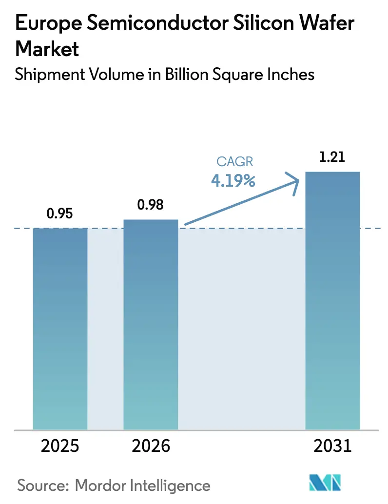
| Base Year Market Size (2025) | 0.95 Billion Square Inches |
| Market Volume (2026) | 0.98 Billion Square Inches |
| Market Volume (2031) | 1.21 Billion Square Inches |
| Growth Rate (2026 - 2031) | 4.19% CAGR |
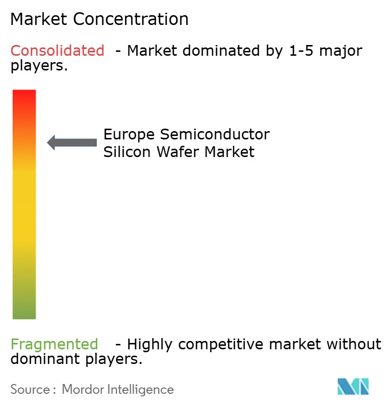
| Market Concentration | High |
Major Players *Disclaimer: Major Players sorted in no particular order Image © Mordor Intelligence. Reuse requires attribution under CC BY 4.0. | |
Europe Semiconductor Silicon Wafer Market Analysis by Mordor Intelligence
The Europe semiconductor silicon wafer market size in terms of shipment volume is projected to expand from 0.95 Billion Square Inches in 2025 and 0.98 Billion Square Inches in 2026 to 1.21 Billion Square Inches by 2031, registering a CAGR of 4.19% between 2026 to 2031. Foundry expansions backed by EU Chips Act incentives are reshaping regional supply, yet Asia continues to dominate commodity substrates, leaving room for European suppliers focused on higher-value-add niches. Automotive electrification and edge-AI adoption are tilting demand toward 300-mm prime-polished and silicon-on-insulator wafers. Power-device migration to 200 mm silicon carbide formats is sustaining a parallel-diameter stream that widens the supplier's addressable volume without cannibalizing 300 mm growth. Competitive dynamics favor incumbents with capital depth, but specialty players that master engineered substrates are capturing design wins vital to 5G, 6G, and quantum computing roadmaps.
Key Report Takeaways
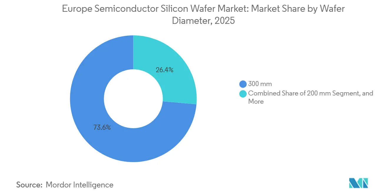
- By wafer diameter, the 300 mm format led with 73.61% of the Europe semiconductor silicon wafer market share in 2025, while also logging the fastest projected expansion at a 4.92% CAGR through 2031.
- By semiconductor device type, logic devices dominated the Europe semiconductor silicon wafer market with a 32.74% share in 2025 and are set to advance at a 5.11% CAGR to 2031.
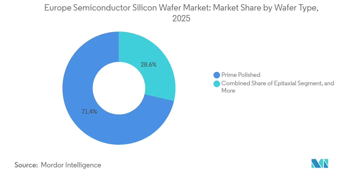
- By wafer type, prime polished substrates accounted for 71.38% of 2025 volume, whereas silicon-on-insulator wafers posted the highest forecast growth at a 4.74% CAGR through 2031.
- By end-user, consumer electronics accounted for 38.49% of shipments in 2025, while automotive applications registered the strongest 4.83% CAGR over the same period.
- By geography, Germany accounted for 27.77% of regional wafer volume in 2025, whereas France recorded the fastest 5.07% annual growth rate through 2031.
Note: Market size and forecast figures in this report are generated using Mordor Intelligence’s proprietary estimation framework, updated with the latest available data and insights as of January 2026.
Worldwide, activity is shaped by contributions from multiple regions, with Europe representing one of the more structurally developed among them. The global report on semiconductor silicon wafer market by Mordor Intelligence reflects how these regional layers combine into a single system.
Europe Semiconductor Silicon Wafer Market Trends and Insights
Drivers Impact Analysis*
| Driver | (~) % Impact on CAGR Forecast | Geographic Relevance | Impact Timeline |
|---|---|---|---|
| Proliferation of 300 mm wafer capacity in European foundries | +1.2% | Germany, France, Italy | Medium term (2-4 years) |
| Growing demand for power electronics in EV and renewable grid | +1.0% | Germany, France, Spain, Austria | Medium term (2-4 years) |
| EU Chips Act incentives for domestic semiconductor manufacturing | +0.9% | Europe-wide, concentrated in Germany, France, Italy | Long term (≥4 years) |
| Adoption of silicon-on-insulator wafers for RF and 5G front-end modules | +0.6% | France, Germany, Netherlands | Short term (≤2 years) |
| Edge AI adoption driving 200 mm logic and analog node revivals | +0.4% | Germany, France, Italy | Medium term (2-4 years) |
| Emerging high-resistivity wafers for quantum computing R&D | +0.1% | Germany, Netherlands, Finland | Long term (≥4 years) |
| Source: Mordor Intelligence | |||
Proliferation of 300 mm Wafer Capacity in European Foundries
New 300 mm greenfield plants are reshaping cost curves for the Europe semiconductor silicon wafer market. GlobalWafers brought Italy's first 300 mm site online in October 2025, with a nameplate output of 1 million wafers per year, of which more than 60% is secured under long-term contracts with STMicroelectronics and Infineon. The European Semiconductor Manufacturing Company joint venture in Dresden will draw an extra 40,000 wafers each month when pilot runs start in late 2027, anchoring regional substrate pull for automotive nodes.[1]TSMC, “ESMC Groundbreaking Ceremony in Dresden,” tsmc.com Siltronic’s Singapore ramp, completed in 2024, also allocates part of its 300 mm output to European buyers facing capacity rationing. Together, these projects lift regional bargaining power on polysilicon pricing and shorten logistics loops for critical automotive and industrial volumes.
Growing Demand for Power Electronics in EV and Renewable Grid
Electrification targets are steering wafer mix toward high-voltage devices fabricated on both silicon and silicon carbide. Infineon began 200 mm SiC processing in Villach during the first quarter of 2025, enabling traction inverters that must handle voltages above 1,200 V.[2]Infineon Technologies, “Infineon Opens New 300 mm Module in Dresden,” infineon.com STMicroelectronics mirrored that move at Catania in the fourth quarter, and onsemi committed up to USD 2 billion for end-to-end SiC capacity in the Czech Republic. EU-backed Transform and related programs are knitting together a European SiC value chain that reduces reliance on Asian ingot suppliers. Demand also comes from grid-scale solar inverters and wind turbines that use ruggedized power modules, thereby driving broader substrate uptake.
EU Chips Act Incentives for Domestic Semiconductor Manufacturing
State-aid packages covering 15%-35% of qualified capex have altered the investment calculus for the Europe semiconductor silicon wafer market. Intel’s Magdeburg megafab and Infineon’s Dresden expansion headline the early wave of Integrated Production Facilities, but material suppliers also benefit. GlobalWafers’ Novara plant and Soitec’s Bernin III line both leveraged national incentive schemes to moderate financing costs.[3]European Court of Auditors, “Special Report: EU Chips Act,” eca.europa.eu The European Court of Auditors cautioned that the bloc may still reach only 11.7% global chip production share by 2030, underscoring persistent cost headwinds despite large grants. Even so, more than EUR 80 billion in announced wafer-and-fab outlays has already been redirected from Asia to Europe.
Adoption of Silicon-On-Insulator Wafers for RF and 5G Front-End Modules
RF-SOI substrates are now ubiquitous in 5G smartphones, and Europe hosts the global leader. Soitec’s technology sits inside every 5G handset shipped in 2026, with Bernin and Pasadena fabs supplying Qorvo, Skyworks, and Broadcom. The European FAMES pilot line is scaling FD-SOI to 7 nm for 6G radios, widening future addressable demand. Premium pricing at two-to-three times bulk silicon expands wafer-maker margins, while national regulators mandating open radio access networks pull incremental SOI volume into Europe.
Restraints Impact Analysis*
| Restraint | (~) % Impact on CAGR Forecast | Geographic Relevance | Impact Timeline |
|---|---|---|---|
| Limited polysilicon feedstock supply within Europe | -0.7% | Europe-wide, acute in Germany, France | Medium term (2-4 years) |
| High capital intensity and long ROI deterring new entrants | -0.5% | Europe-wide | Long term (≥4 years) |
| Geopolitical dependency on Asia for wafer processing equipment | -0.3% | Europe-wide | Short term (≤2 years) |
| Environmental regulations increasing cost of ultrapure water usage | -0.2% | Germany, France, Netherlands, Belgium | Medium term (2-4 years) |
| Source: Mordor Intelligence | |||
Limited Polysilicon Feedstock Supply within Europe
Wacker Chemie’s July 2025 etching-line expansion lifted regional semiconductor-grade polysilicon output by more than 50% but Europe still imports over 70% of feedstock from Asia. Heavy reliance on external sources exposes wafer makers to geopolitical shocks and price spikes. Building an integrated silicon carbide supply under the Transform program shows the scale of capital and environmental permitting hurdles that constrain upstream diversification. Until additional purification capacity comes online or binding long-term offtake deals are signed, feedstock tightness will cap upside for European wafer shipments.
High Capital Intensity and Long ROI Deterring New Entrants
A new 300 mm substrate fab costs between USD 3 billion and USD 5 billion for mature nodes and USD 10 billion or more for leading-edge grades, with payback stretching 7-10 years. GlobalWafers’ EUR 2 billion Novara build illustrates both the financial heft and multi-year timeline needed just to achieve first silicon. Even with state subsidies offsetting up to one-third of capital outlays, demand cyclicality and swings in wafer pricing deter newcomers without deep balance sheets. The result is an oligopolistic structure that entrenches the five incumbent giants in the Europe semiconductor silicon wafer market.
*Our forecasts treat driver/restraint impacts as directional, not additive. The impact forecasts reflect baseline growth, mix effects, and variable interactions.
Segment Analysis
By Wafer Diameter: Volume Clusters At 300 mm, Specialty Growth At 200 mm
The 300 mm node delivered 73.61% of shipments in 2025, confirming its position as the workhorse format for logic and memory processes that dominate European fab roadmaps. GlobalWafers’ Novara launch and the forthcoming ESMC Dresden ramp collectively add more than 1.5 million wafers to the annual 300 mm capacity, deepening the Europe semiconductor silicon wafer market for prime-polished substrates. Cost-per-die advantages, compatibility with EUV lithography, and tight coupling to automotive-qualified process flows keep 300 mm utilisation high.
Parallel demand for 200 mm persists, propelled by silicon carbide power devices and analog products tailored to automotive electrification. Infineon’s Villach and STMicroelectronics’ Catania conversions prove that crystal-growth realities and defect budgets still favor 200 mm for SiC wafers. Consequently, the Europe semiconductor silicon wafer market retains a dual-diameter structure where 300 mm drives volume and 200 mm secures margin resilience, while up to 150 mm lines remain focused on MEMS and optoelectronic niches served by Okmetic’s sensor-grade output.


By Semiconductor Device Type: Logic Anchors Share, Power Discretes Speed Growth
Logic wafers represented 32.74% of 2025 volume, benefiting from edge-AI accelerators and automotive microcontrollers that rely on 28 nm-65 nm nodes, processes that European fabs are adding at scale. The Dresden joint venture between TSMC, Bosch, Infineon, and NXP focuses on precisely those geometries, which should widen the Europe semiconductor silicon wafer market size allocated to logic over the forecast horizon.
Memory holds a smaller slice due to Europe’s limited commodity DRAM output, yet embedded non-volatile memory tied to FD-SOI projects keeps niche growth alive. Analog and mixed-signal devices ride industrial automation and sensor interface demand, while silicon carbide discretes for high-voltage drives are the fastest climber in the Europe semiconductor silicon wafer market, spurring a wave of epitaxial wafer orders from power-device manufacturers.
By Wafer Type: Prime Polished Still Dominant, SOI Sets Premium Pace
In 2025, the establishment of secure capacity contracts between Siltronic, GlobalWafers, and integrated device manufacturers in Europe played a crucial role in enabling prime polished substrates to account for 71.38% of the regional volume. High-throughput production lines play a pivotal role in significantly improving the predictability of cost roadmaps and act as a fundamental cornerstone for mainstream fabrication facilities, ensuring efficiency and reliability in operations.
Silicon-on-insulator, however, records the quickest 4.74% trajectory thanks to Soitec’s RF-SOI and FD-SOI portfolios. Every 5G smartphone shipped globally contains RF-SOI, and the move to 6G millimeter-wave antennas multiplies layer-stack requirements, expanding the Europe semiconductor silicon wafer market share for engineered substrates. Epitaxial and specialty silicon continue to serve power and quantum segments where defect density and resistivity control substitute for wafer diameter as the decisive parameter.
By End-User: Consumer Electronics Provides Base Load, Automotive Lifts CAGR
Consumer electronics accounted for 38.49% of 2025 shipments, supplying smartphones, PCs, and servers that already rely on mature 300 mm logic and memory lines, stabilizing baseline volume for the Europe semiconductor silicon wafer market. Although the growth in handset unit shipments has plateaued, the increasing complexity of RF front-end components is mitigating the impact of this stagnation. This trend is ensuring a consistent and robust demand for substrates in the market.
Automotive is the standout growth vertical, expanding at 4.83% through 2031 as electrified drivetrains and advanced driver-assistance systems double or triple silicon content per vehicle. Villach, Catania, and emerging Czech SiC capacity funnel dedicated wafer streams into traction inverters, onboard chargers, and power management ICs. Telecommunications infrastructure and industrial automation also add incremental lifts, but their diversity makes automotive the most predictable upside driver.
Geography Analysis
Germany commands nearly 27.77% of regional wafer volume on the strength of Siltronic’s Freiberg and Burghausen hubs, Infineon’s Dresden cluster, and Wacker’s expanded polysilicon refinery. The EUR 10 billion Dresden mega-fab, co-owned by TSMC, Bosch, Infineon, and NXP, is set to deliver 40,000 additional 300 mm wafers each month from late 2027, reinforcing Germany’s central role in the European semiconductor silicon wafer market. Policy alignment across federal and state levels keeps land, power, and workforce pipelines in sync with investment rollouts.
France posts the fastest growth rate at 5.07%, anchored by Soitec’s Bernin III expansion and STMicroelectronics’ upgrades at Crolles and Rousset. The EUR 433 million FAMES pilot line places France at the leading edge of FD-SOI scaling, giving the country strategic leverage over engineered-substrate supply chains sought by global handset and infrastructure OEMs. Tax credits and streamlined environmental approvals shorten time-to-volume for both wafer and device projects, feeding virtuous capacity cycles.
Italy, Spain, and the United Kingdom round out expansion nodes that diversify continental risk. Italy’s Novara 300 mm launch creates the country’s first large-diameter footprint, Spain’s Málaga research lines reinforce collaborative 300 mm prototyping with Imec, and a UK-Bulgaria consortium is adding silicon carbide volume aimed at automotive and renewable grids. Central Europe draws power-device assets as onsemi deploys up to USD 2 billion in the Czech Republic, illustrating how multiple nations capitalize on localized incentives to build complementary wafer specialties.
Mordor Intelligence provides coverage of the semiconductor silicon wafer market across other key regional markets, including North America and Asia, each with their regulatory frameworks and demand patterns. Detailed country-level analysis extends to Germany, South Korea, Taiwan, United States, Japan, India, and China incorporating local coverage and market participation, as required.
Competitive Landscape
The Europe semiconductor silicon wafer market is moderately concentrated around five global suppliers. Shin-Etsu, SUMCO, GlobalWafers, Siltronic, and SK Siltron collectively control more than 85% of the installed 300 mm capacity. Their scale secures favorable polysilicon contracts and volume pricing on wafer processing equipment. Soitec holds a near-monopoly on radio-frequency silicon-on-insulator substrates used in every 5G smartphone. Smaller specialty vendors focus on sensor-grade or high-resistivity material to avoid direct price competition.
GlobalWafers started Italy’s first 300 mm plant in October 2025, locking multi-year supply deals with STMicroelectronics and Infineon. Siltronic lifted its global 300 mm output 15% after its Singapore ramp and channels part of that volume to European automotive nodes. Infineon opened a new 300 mm power module in Dresden in January 2026, boosting internal wafer pull by 20%. Soitec is expanding Bernin III to add 300 mm SOI capacity aimed at 6G and photonics applications. onsemi committed up to USD 2 billion for a silicon carbide value chain in the Czech Republic that covers ingot growth through module packaging.
Backward integration by device makers is raising competitive pressure on merchant wafer vendors. High capital intensity and seven-year payback periods still deter most new entrants, preserving oligopolistic pricing discipline. Engineered substrates for quantum computing and wide-bandgap power devices offer growth opportunities for companies with limited portfolios. Continued dependence on non-European equipment suppliers, however, exposes all players to geopolitical and export-control risks.
Europe Semiconductor Silicon Wafer Industry Leaders
Shin-Etsu Chemical Co., Ltd.
SUMCO Corporation
GlobalWafers Co., Ltd.
Siltronic AG
SK siltron Co., Ltd.
- *Disclaimer: Major Players sorted in no particular order

Recent Industry Developments
- February 2026: The NanoIC pilot line in Grenoble, France, commenced operations with EUR 2.5 billion (USD 2.82 billion) in public and private investment, supplying 300 mm packaging and heterogeneous integration services.
- January 2026: Infineon opened a new 300 mm power-semiconductor module in Dresden, lifting site capacity by 20%.
- October 2025: GlobalWafers launched Italy’s first 300 mm wafer plant in Novara, delivering 1 million wafers per year under multi-year contracts.
- October 2025: GlobalFoundries announced a multi-billion-euro plan to expand its Dresden fab with additional 300 mm capacity for automotive and industrial clients.


Europe Semiconductor Silicon Wafer Market Report Scope
The Europe Semiconductor Silicon Wafer Market Report is Segmented by Wafer Diameter (Up to 150 mm, 200 mm, 300 mm), Semiconductor Device Type (Logic, Memory, Analog, Discrete, Optoelectronics, Sensors, Micro), Wafer Type (Prime Polished, Epitaxial, Silicon-on-Insulator, Specialty Silicon), End-User (Consumer Electronics, Industrial, Telecommunications, Automotive, Other End-User Applications), and Country (Germany, France, United Kingdom, Italy, Spain, Russia, Rest of Europe). The Market Forecasts are Provided in Terms of Shipments by Volume (Square Inches).
| Up to 150 mm |
| 200 mm |
| 300 mm |
| Logic |
| Memory |
| Analog |
| Discrete |
| Optoelectronics |
| Sensors |
| Micro (MCU, MPU, DSP) |
| Prime Polished |
| Epitaxial |
| Silicon-on-Insulator (SOI) |
| Specialty Silicon (High-Resistivity, Power, Sensor-Grade) |
| Consumer Electronics | Mobile and Smartphones |
| PCs and Servers | |
| Industrial | |
| Telecommunications | |
| Automotive | |
| Other End-User Applications |
| Germany |
| France |
| United Kingdom |
| Italy |
| Spain |
| Russia |
| Rest of Europe |
| By Wafer Diameter | Up to 150 mm | |
| 200 mm | ||
| 300 mm | ||
| By Semiconductor Device Type | Logic | |
| Memory | ||
| Analog | ||
| Discrete | ||
| Optoelectronics | ||
| Sensors | ||
| Micro (MCU, MPU, DSP) | ||
| By Wafer Type | Prime Polished | |
| Epitaxial | ||
| Silicon-on-Insulator (SOI) | ||
| Specialty Silicon (High-Resistivity, Power, Sensor-Grade) | ||
| By End-User | Consumer Electronics | Mobile and Smartphones |
| PCs and Servers | ||
| Industrial | ||
| Telecommunications | ||
| Automotive | ||
| Other End-User Applications | ||
| By Country | Germany | |
| France | ||
| United Kingdom | ||
| Italy | ||
| Spain | ||
| Russia | ||
| Rest of Europe | ||


Key Questions Answered in the Report
How large is the Europe semiconductor silicon wafer market in 2026?
It stands at 989.86 million square inches in 2026 with a 4.19% CAGR projected through 2031.
Which wafer diameter accounts for the bulk of European shipments?
300 mm substrates lead with 73.61% share in 2025 and remain the primary volume driver to 2031.
What segment grows fastest within wafer types?
Silicon-on-insulator wafers post the quickest 4.74% CAGR, fueled by 5G and future 6G RF modules.
Why is automotive demand important for wafer suppliers?
Electrification and ADAS triple silicon content per vehicle, pushing automotive wafer demand up 4.83% annually.
How do EU Chips Act incentives influence wafer capacity?
Grants covering up to 35% of capex reduce financing hurdles, redirecting more than EUR 80 billion of planned wafer and fab investments into Europe.
Which countries are emerging beyond Germany and France?
Italy, Spain and the United Kingdom are adding greenfield 300 mm and silicon carbide sites that diversify regional substrate supply.
Page last updated on:


