Germany Semiconductor Silicon Wafer Market Size and Share
Market Overview
| Study Period | 2020 - 2031 |
|---|---|
| Forecast Data Period | 2026 - 2031 |
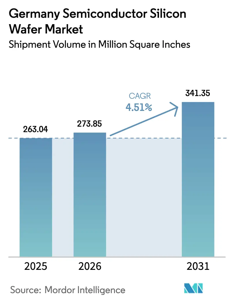
| Base Year Market Size (2025) | 263.04 Million Square Inches |
| Market Volume (2026) | 273.85 Million Square Inches |
| Market Volume (2031) | 341.35 Million Square Inches |
| Growth Rate (2026 - 2031) | 4.51% CAGR |
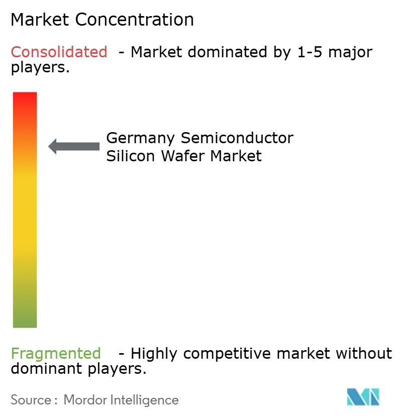
| Market Concentration | High |
Major Players *Disclaimer: Major Players sorted in no particular order Image © Mordor Intelligence. Reuse requires attribution under CC BY 4.0. | |
Germany Semiconductor Silicon Wafer Market Analysis by Mordor Intelligence
The Germany semiconductor silicon wafer market size in terms of shipment volume was valued at 263.04 Million Square Inches in 2025 and is estimated to grow from 273.85 Million Square Inches in 2026 to reach 341.35 Million Square Inches by 2031, at a CAGR of 4.51% during the forecast period (2026-2031). A multi-year build-out of 300 mm logic and power-device fabs, anchored by Intel, TSMC, Infineon, and GlobalFoundries, is lifting long-term demand for prime polished and epitaxial substrates while tightening contract pricing. Corporate power-purchase agreements for wind and solar electricity are beginning to close the historical energy-cost gap with Asia, strengthening the competitiveness of Germany's semiconductor silicon wafer market. Parallel shifts toward float-zone high-purity wafers for quantum initiatives and fully depleted SOI for automotive radar add specialty upside. At the same time, volatile polysilicon pricing and elevated industrial tariffs keep near-term margins under pressure, compelling producers to prioritize high-value segments and long-term offtake contracts.
Key Report Takeaways
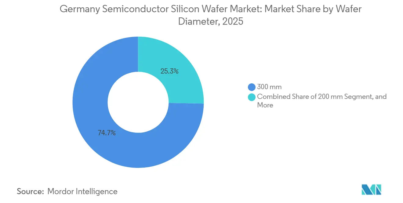
- By wafer diameter, the 300 mm segment led with 74.68% of the Germany semiconductor silicon wafer market share in 2025 and is set to advance at a 4.98% CAGR through 2031.
- By semiconductor device type, logic accounted for 36.82% in 2025 and is projected to grow at a 5.06% CAGR through 2031.
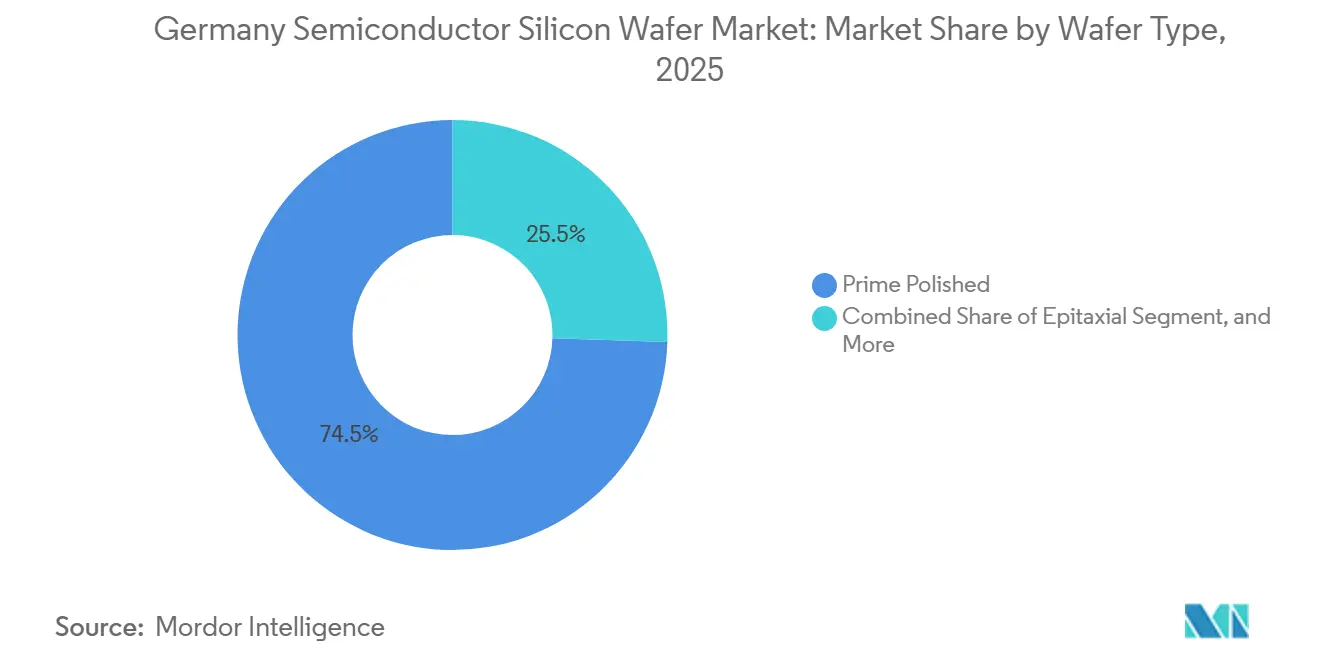
- By wafer type, prime polished accounted for 74.49% of the Germany semiconductor silicon wafer market share in 2025, while silicon-on-insulator substrates are forecast to grow the fastest at a 5.15% CAGR through 2031.
- By end-user, consumer electronics commanded a 41.74% of the Germany semiconductor silicon wafer market share in 2025, whereas automotive applications are expected to record the highest growth at a 5.09% CAGR to 2031.
Note: Market size and forecast figures in this report are generated using Mordor Intelligence’s proprietary estimation framework, updated with the latest available data and insights as of January 2026.
Germany contributes to a system defined not by any single country or region but by the interaction of many. The global semiconductor silicon wafer market data by Mordor Intelligence represents that combined structure.
Germany Semiconductor Silicon Wafer Market Trends and Insights
Drivers Impact Analysis*
| Driver | (~) % Impact on CAGR Forecast | Geographic Relevance | Impact Timeline |
|---|---|---|---|
| Strong CAPEX Pipeline for 300 mm Fab Expansions in Germany | +1.8% | Germany, spill-over to broader EU supply chains | Medium term (2-4 years) |
| Revival of Automotive Chip Demand Post-2025 | +1.2% | Germany, with secondary effects in Central and Eastern Europe | Medium term (2-4 years) |
| EU Chips Act Incentives for On-shore Wafer Production | +1.0% | Germany, France, Italy, Netherlands | Long term (≥4 years) |
| Increasing Adoption of Power Devices for E-Mobility | +0.9% | Germany, France, Sweden, export demand in China and North America | Long term (≥4 years) |
| Shift Toward Float-Zone High-Purity Wafers for Quantum-Tech | +0.3% | Germany, Netherlands, France | Long term (≥4 years) |
| Corporate PPAs Driving Renewable-Powered Wafer Plants | +0.2% | Germany, Spain, Denmark | Short term (≤2 years) |
| Source: Mordor Intelligence | |||
Strong Capex Pipeline for 300 Mm Fab Expansions in Germany
Intel broke ground on two Magdeburg fabs in mid-2025 as part of a EUR 30 billion (USD 34 billion) commitment that will deliver sub-5 nm logic capacity when production starts in 2028.[1]Intel Corporation, “Intel Confirms Magdeburg Investment,” intel.com TSMC, Bosch, Infineon, and NXP jointly launched the European Semiconductor Manufacturing Company in Dresden, a EUR 10 billion (USD 11.3 billion) venture slated to produce 40,000 wafers per month at 28 nm, 22 nm, and 16 nm nodes by 2027. Infineon’s EUR 5 billion (USD 5.7 billion) Smart Power Fab, which entered pilot output in early 2025, targets silicon carbide and high-voltage silicon on 300 mm lines. GlobalFoundries is adding more than 1 million 300 mm wafers per year to its Dresden plant through a EUR 1.1 billion (USD 1.25 billion) expansion that was completed in 2028. Collectively, these projects compress polished-wafer lead times and secure multi-year offtake agreements that underpin the market’s long-term growth trajectory.
Revival of Automotive Chip Demand Post-2025
German vehicle output rebounded to 4.1 million units in 2024, restoring chip orders that had stalled during the 2022-2023 inventory correction. Infineon reported double-digit growth in power-device shipments for electric-vehicle drivetrains during fiscal 2025, with silicon carbide MOSFETs delivering 3% efficiency gains over silicon IGBTs in production models such as the Porsche Taycan.[2]Infineon Technologies, “Smart Power Fab Press Release,” infineon.com Demand is reinforced by the shift to 800 V battery systems that require high-voltage epitaxial wafers with sub-2% doping variation. Euro 7 rules, effective 2025, require multiple sensors and microcontrollers per car, further increasing wafer volume requirements. As automakers lock in supply, wafer sellers benefit from longer contracts and tighter specification premiums.
EU Chips Act Incentives for On-Shore Wafer Production
The European Chips Act earmarks about EUR 15 billion (USD 17 billion) for substrates and front-end materials, covering up to 35% of eligible capex for “first-of-a-kind” facilities.[3]European Commission, “European Chips Act Overview,” ec.europa.eu Germany secured the largest share, channeling more than EUR 10 billion (USD 11.3 billion) in grants and tax credits to Intel, TSMC, and Infineon. The legislation also mandates resilience audits that require fabs to source at least 40% of critical materials from European suppliers by 2030, prompting wafer makers to partner with domestic polysilicon refiners. Although approval cycles stretch 18-24 months, the subsidies materially narrow Germany’s 15-20% cost gap versus Asian sites. The result is a stronger local ecosystem that reduces transcontinental logistics risk for high-value chips.
Increasing Adoption of Power Devices for E-Mobility
Electric-vehicle penetration in Germany climbed to 18.4% of new registrations in 2025, doubling semiconductor content per car relative to 2020 levels. Silicon carbide MOSFETs for inverters and gallium nitride HEMTs for on-board chargers depend on epitaxial wafers with micropipe densities below 0.5 cm-², specifications that only a handful of suppliers can meet. Infineon’s Smart Power Fab is calibrated for this demand, integrating both 200 mm SiC and 300 mm silicon lines under one roof. As automakers adopt 800 V architectures, wafer demand scales in lockstep with higher voltage classes and stricter defect ceilings. Long-term EV targets under Germany’s Energiewende policy guarantee durable volume for power-grade substrates.
Restraints Impact Analysis*
| Restraint | (~) % Impact on CAGR Forecast | Geographic Relevance | Impact Timeline |
|---|---|---|---|
| Volatile Polysilicon Pricing | -0.7% | Global, acute impact on European cost structures | Short term (≤2 years) |
| High Energy Costs Versus Asian Peers | -0.5% | Germany, Belgium, Netherlands | Medium term (2-4 years) |
| Talent Shortage in Crystal-Growing Specialists | -0.3% | Germany, France, Austria | Long term (≥4 years) |
| Tightening ESG Audits on Scope-3 Emissions | -0.2% | Germany, France, Netherlands | Medium term (2-4 years) |
| Source: Mordor Intelligence | |||
Volatile Polysilicon Pricing
Semiconductor-grade polysilicon plunged from USD 35 kg⁻¹ in early 2022 to USD 6.5 kg⁻¹ by December 2024 after Chinese suppliers added 400,000 t of annual capacity. Siltronic said raw-material costs fell 12% in H1 2025 but warned that spot quotes remain 40% beneath long-term contract floors, clouding investment planning. A rapid rebound toward USD 20 kg⁻¹ would slice 3-5 percentage points from wafer-maker margins unless device customers accept price increases. The unpredictability deters smaller producers from green-lighting new Czochralski pullers, effectively consolidating share with vertically integrated rivals that refine their own feedstock. Until pricing stabilizes, the supply base will stay cautious on incremental capacity.
High Energy Costs Versus Asian Peers
German industrial electricity averaged EUR 0.18-0.22 kWh⁻¹ in 2025, roughly double Taiwanese and Korean rates, raising total wafer production costs by 6-8%. Continuous crystal pulling at 1,420 °C for 48-72 hours makes energy the second-largest variable expense after polysilicon. Siltronic’s 60 GWh solar PPA with Axpo trims only 5% of its consumption, while Infineon’s 770 GWh renewable portfolio demonstrates the scale required for meaningful relief. Upfront grid-connection costs and renewable intermittency still limit full parity with Asian benchmarks. Consequently, German wafer makers funnel resources into high-margin specialty products where energy intensity carries less weight in the overall cost stack.
*Our forecasts treat driver/restraint impacts as directional, not additive. The impact forecasts reflect baseline growth, mix effects, and variable interactions.
Segment Analysis
By Wafer Diameter: Economies Of Scale Cement 300 mm Leadership
The Germany semiconductor silicon wafer market recorded 300 mm substrates at a commanding 74.68% volume share in 2025, outstripping all other diameters. Tooling for leading-edge logic and automotive power devices is standardized around this format, which delivers more than twice the usable die area of 200 mm alternatives, trimming per-chip processing cost by roughly 30%. Intel’s Magdeburg fabs impose site-flatness below 0.08 µm and total-thickness variation under 0.15 µm, specifications that narrow the approved-vendor list to Shin-Etsu and SUMCO’s premium grades.
Contract prices for 300 mm prime-polished wafers rose to low-to-mid single digits year over year in 2025 as crystal-puller lead times stretched to 24 months. The 200 mm tier retains strategic relevance for analog, MEMS, and discrete manufacturing; X-FAB’s Erfurt line, fully dedicated to 200 mm, captures industrial sensor demand where die sizes exceed 10 mm². Diameters of 150 mm and below are largely confined to legacy optoelectronics, and capacity is expected to consolidate further as vendors rationalize older furnaces.


By Semiconductor Device Type: Logic Drives Volume, Power Devices Accelerate
Logic wafers accounted for 36.82% of 2025 shipments, reflecting Germany’s transition toward edge AI controllers and integrated automotive domain processors. TSMC’s Dresden plant alone will process 40,000 300 mm wafers a month at 28 nm, 22 nm, and 16 nm, cementing logic’s pull on prime-polished supply. Memory’s footprint remains smaller because Germany hosts limited DRAM or NAND front-end capacity, yet data-center growth is spurring tentative interest in specialty memory tie-ups.
Analog and mixed-signal devices, essential for industrial sensor arrays, consumed over one-fifth of wafer volume, aided by Industry 4.0 rollouts. Discrete and power components, including silicon carbide MOSFETs for EV drivetrains, command premium unit pricing, helping producers offset softer consumer-electronics margins. The convergence of logic and analog in fully depleted SOI platforms further blurs device-type boundaries and increases process-flow flexibility.
By Wafer Type: SOI Emerges As Fastest-Growing Niche
Prime polished wafers dominated at 74.49% in 2025, but silicon-on-insulator volumes are growing faster than any other category. Automotive radar and battery-management units require low leakage and latch-up immunity, which are intrinsic to SOI’s buried-oxide structure, making FD-SOI the preferred substrate at 28 nm and 22 nm. Epitaxial wafers accounted for about 18% of shipments, driven by the need for precision-doped layers in silicon carbide and gallium nitride devices.
Specialty silicon, including high-resistivity radio-frequency material and float-zone quantum-grade substrates, accounts for the remaining volume yet delivers outsized margins. GlobalWafers and Topsil released isotopically enriched ²⁸Si float-zone wafers in early 2026, opening a premium micro-segment serving quantum research centers. Hybrid products such as Soitec’s SmartSiC, which bonds SiC epitaxy onto a silicon handle, illustrate continuing innovation in substrate engineering.
By End-User: Automotive Growth Outpaces Consumer Electronics Scale
Consumer electronics retained the largest slice of volume at 41.74% in 2025, buoyed by steady demand for smartphones, PCs, and white goods. However, automotive usage is climbing at the fastest clip, thanks to higher semiconductor content per electric vehicle, rising from about USD 600 in 2024 to a projected USD 1,200 by 2030. Each EV adds multiple radar modules, lidar units, and high-voltage inverters, swelling both logic and power-device wafer pulls.
The industrial automation, telecommunications, and medical sectors provide a diversified layer of mid-single-digit growth, which plays a significant role in mitigating the effects of cyclicality. Automotive customers, who demand impeccable reliability over lifespans of up to 15 years, have become increasingly attractive to wafer suppliers. These customers are willing to adhere to stricter specification requirements and maintain stable pricing, aligning well with wafer suppliers' objectives of achieving predictable and stable returns.
Geography Analysis
Germany anchors roughly 60% of European wafer demand, a position reinforced by a EUR 45 billion (USD 51 billion) cluster of announced 300 mm fabs in Saxony and Saxony-Anhalt. Siltronic’s dual sites in Freiberg and Burghausen delivered about 180 million square inches of 300 mm material in 2024 and are evaluating expansions synchronized with nearby greenfield logic lines. Industrial electricity tariffs remain twice Asian benchmarks, yet large-scale renewable PPAs, such as Infineon’s 770 GWh portfolio, are narrowing the gap and improving long-term cost visibility.
France ranks second, driven by Soitec’s Bernin SOI hub and STMicroelectronics’ Crolles line, which serve automotive and industrial sectors that need radiation-tolerant, low-power logic. Italy, via STMicroelectronics’ Agrate and Catania fabs, focuses on power semiconductors and MEMS on 200 mm wafers, preserving demand for legacy diameters even as European capacity skews 300 mm. The Netherlands, while manufacturing-constrained, exerts technology influence through ASML and NXP, prompting wafer suppliers to maintain regional stockpoints for quick-turn shipments.
Central and Eastern Europe are emerging as assembly and test footholds, but the absence of front-end wafer capacity obliges cross-border logistics that add low-single-digit cost premiums. EU-funded IPCEI programs aim to bridge this gap, yet protracted approvals slow capital deployment. Germany’s Energiewende targets and Euro 7 regulations reinforce automotive and renewable-energy semiconductor use, anchoring the Germany semiconductor silicon wafer market as Europe’s keystone through 2031.
The semiconductor silicon wafer market is analyzed by Mordor Intelligence across multiple other geographies, with in-depth regional assessments available for Europe, North America, and Asia. This is complemented by country-specific insights for United States, Taiwan, South Korea, Japan, India, and China, reflecting various localized market behavior and policy environments' coverage.
Competitive Landscape
Siltronic, Shin-Etsu, SUMCO, and GlobalWafers collectively supply about three-quarters of Germany’s 300 mm polished wafer volume, resulting in moderate market concentration. Siltronic’s Singapore expansion will inject 1.5 million wafers per year by 2027, largely earmarked for captive German automotive clients under multi-year agreements with 3-5% annual escalators. Shin-Etsu and SUMCO leverage in-house polysilicon operations to retain a cost advantage between 6-8% relative to merchant peers, a margin cushion that widens during feedstock volatility.
Soitec maintains roughly 80% of the global SOI substrate market share, protected by its Smart Cut patent estate, which exceeds 3,000 filings, ensuring sustained royalty leverage. Device manufacturers increasingly pursue partial vertical integration; Infineon’s move into silicon carbide epitaxy captures an additional 30-40% of the value chain and tightens its grip on high-voltage EV inverters. Chinese entrants, including Zhonghuan Semiconductor, offer 10-15% lower pricing, but EU supply-chain resilience rules that target a 40% domestic-sources threshold by 2030 limit rapid penetration.
Market participants are now diverging their strategies: some are focusing on scaling operations to increase polished wafer volumes, while others are concentrating on specialized segments such as silicon-on-insulator (SOI), float-zone, or power-grade applications. The persistent shortage of skilled talent in crystal pulling and metrology further exacerbates the challenges in the industry. This situation provides a competitive advantage to established players who possess the financial resources to invest in comprehensive training programs and advanced automation technologies, enabling them to sustain high yield levels.
Germany Semiconductor Silicon Wafer Industry Leaders
Siltronic AG
Shin-Etsu Handotai Co., Ltd.
SUMCO Corporation
GlobalWafers Co., Ltd.
Soitec S.A.
- *Disclaimer: Major Players sorted in no particular order

Recent Industry Developments
- January 2026: GlobalWafers and Topsil advanced isotopically enriched ²⁸Si float-zone wafers, achieving coherence times over 200 µs on 200 mm and 300 mm formats for German quantum initiatives.
- December 2025: Infineon reached 100% green electricity across global operations through PPAs totaling 770 GWh annually, covering Dresden, Regensburg and Warstein fabs.
- November 2025: Siltronic posted Q3 2025 revenue of EUR 383.7 million (USD 434 million), up 4.8% YoY, and confirmed its Singapore 300 mm expansion remains on schedule.
- August 2025: TSMC, Bosch, Infineon and NXP inaugurated the EUR 10 billion (USD 11.3 billion) European Semiconductor Manufacturing Company in Dresden, set for 40,000 wpm production in 2027.


Germany Semiconductor Silicon Wafer Market Report Scope
The Germany Semiconductor Silicon Wafer Market Report is Segmented by Wafer Diameter (Up to 150 mm, 200 mm, 300 mm), Semiconductor Device Type (Logic, Memory, Analog, Discrete, Other Semiconductor Device Types), Wafer Type (Prime Polished, Epitaxial, Silicon-on-Insulator (SOI), Specialty Silicon), End-user (Consumer Electronics, Mobile and Smartphones, PCs and Servers, Industrial, Telecommunications, Automotive, Other End-user Applications). The Market Forecasts are Provided in Terms of Shipments by Volume (Square Inches).
| Up to 150 mm |
| 200 mm |
| 300 mm |
| Logic |
| Memory |
| Analog |
| Discrete |
| Other Semiconductor Device Types (Optoelectronics, Sensors, Micro) |
| Prime Polished |
| Epitaxial |
| Silicon-on-Insulator (SOI) |
| Specialty Silicon (High-Resistivity, Power, Sensor-Grade) |
| Consumer Electronics |
| Mobile and Smartphones |
| PCs and Servers |
| Industrial |
| Telecommunications |
| Automotive |
| Other End-user Applications |
| By Wafer Diameter | Up to 150 mm |
| 200 mm | |
| 300 mm | |
| By Semiconductor Device Type | Logic |
| Memory | |
| Analog | |
| Discrete | |
| Other Semiconductor Device Types (Optoelectronics, Sensors, Micro) | |
| By Wafer Type | Prime Polished |
| Epitaxial | |
| Silicon-on-Insulator (SOI) | |
| Specialty Silicon (High-Resistivity, Power, Sensor-Grade) | |
| By End-user | Consumer Electronics |
| Mobile and Smartphones | |
| PCs and Servers | |
| Industrial | |
| Telecommunications | |
| Automotive | |
| Other End-user Applications |


Key Questions Answered in the Report
How fast is the Germany semiconductor silicon wafer market growing between 2026-2031?
The market is projected to advance at a 4.51% CAGR, moving from 273.85 million square inches in 2026 toward 341.35 million square inches by 2031.
Why are 300 mm wafers so dominant in Germany?
Major greenfield fabs from Intel, TSMC and Infineon are optimized for 300 mm tools, which deliver more die per pass and about 30% lower processing cost per chip than 200 mm alternatives.
Which wafer type shows the fastest growth?
Silicon-on-insulator leads growth with a 5.15% CAGR as automotive radar, battery-management units and industrial IoT devices demand low-leakage, radiation-tolerant substrates.
How do high German electricity prices affect wafer makers?
Tariffs double those in Taiwan or South Korea inflate production costs by 6-8%, pushing suppliers toward long-term renewable PPAs and higher-margin specialty products.
What impact does the EU Chips Act have on local wafer capacity?
The Act de-risks investments by funding up to 35% of capex for new fabs and substrates, accelerating expansions but adding administrative lead times of up to two years.
Which end-user segment will grow fastest through 2031?
Automotive applications, underpinned by rising electric-vehicle penetration and ADAS adoption, are forecast to expand at a 5.09% CAGR, outpacing all other sectors.
Page last updated on:


