Profilometer Market Size and Share
Market Overview
| Study Period | 2020 - 2031 |
|---|---|
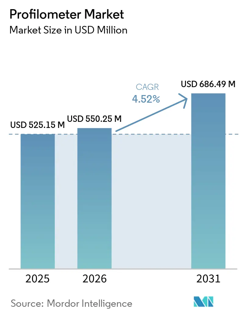
| Market Size (2026) | USD 550.25 Million |
| Market Size (2031) | USD 686.49 Million |
| Growth Rate (2026 - 2031) | 4.52% CAGR |
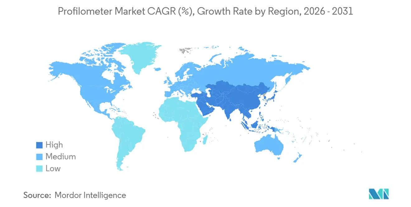
| Fastest Growing Market | Asia Pacific |
| Largest Market | Asia Pacific |
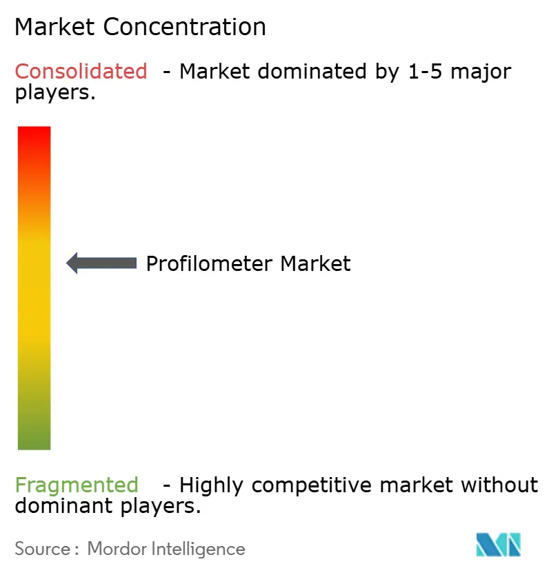
| Market Concentration | Medium |
Major Players *Disclaimer: Major Players sorted in no particular order Image © Mordor Intelligence. Reuse requires attribution under CC BY 4.0. | |
Profilometer Market Analysis by Mordor Intelligence
The profilometer market size is expected to increase from USD 525.15 million in 2025 to USD 550.25 million in 2026 and reach USD 686.49 million by 2031, growing at a CAGR of 4.52% over 2026-2031. This trajectory is fueled by semiconductor device geometries below 2 nm, adoption of hybrid bonding, and a broad pivot from contact-based stylus instruments toward non-contact three-dimensional optical solutions that deliver sub-nanometer vertical resolution in seconds. Rising requirements for inline inspection, wider adoption in healthcare and additive manufacturing, and integration with Industry 4.0 data platforms are expanding the addressable market for profilometers beyond traditional quality-control labs. Competitive strategies revolve around multi-sensor integration, machine-learning-enabled surface classification, and acquisitions that bring software ecosystems, calibration know-how, and automation interfaces under one roof. Persistent headwinds include the capital burden of advanced optical systems, dependence on fragile rare-earth supply chains, and lingering fragmentation of surface-texture standards across verticals, which together temper the profilometer market’s near-term growth pace.
Key Report Takeaways
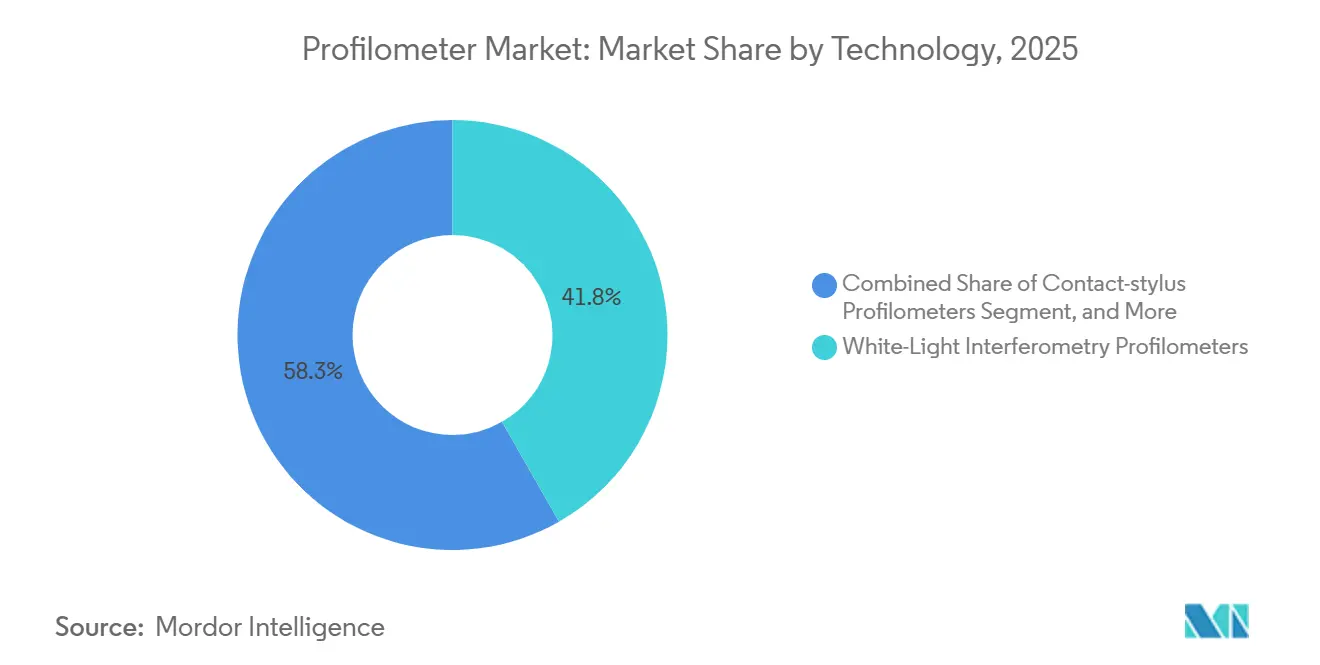
- By technology, White-Light Interferometry Profilometers led the market with 41.75% of the profilometer market in 2025 revenue, whereas Chromatic Confocal and Fringe-Projection Profilometers will expand at a 5.23% CAGR through 2031, underscoring the migration toward inline, high-speed inspection.
- By measurement dimension, 3-D Areal Profilometry held 58.31% of the profilometer market share in 2025 and is advancing at a 5.11% CAGR through 2031.
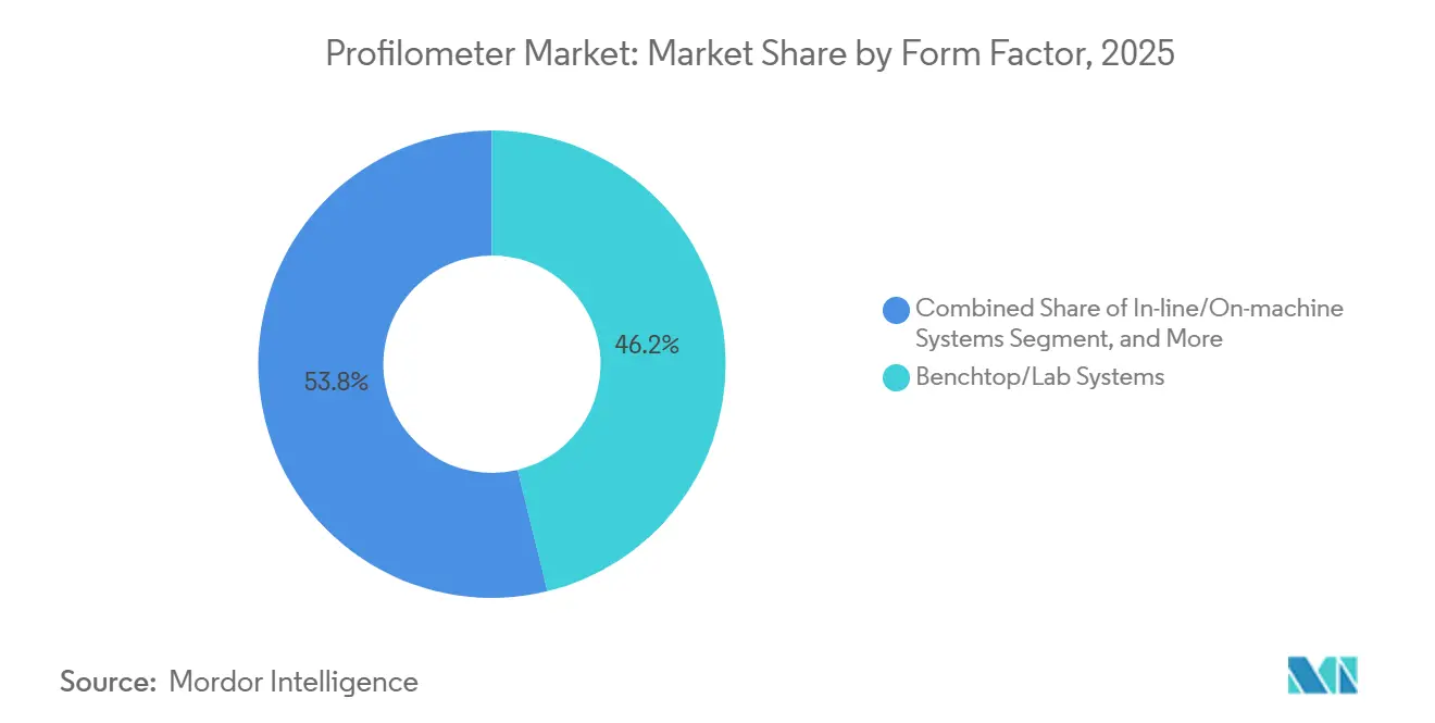
- By form factor, Benchtop/Lab Systems commanded 46.19% share in 2025, while In-Line/On-Machine Systems are projected to post a 4.99% CAGR to 2031.
- By end-use industry, healthcare represented the fastest expansion, registering a 5.29% CAGR to 2031, even as semiconductor and electronics retained the largest 2025 share of 34.82%.
- By geography, Asia-Pacific, while maintaining the largest market share of 37.53% in 2025, is projected to experience the most rapid growth, with a CAGR of 4.38% anticipated through to 2031.
Note: Market size and forecast figures in this report are generated using Mordor Intelligence’s proprietary estimation framework, updated with the latest available data and insights as of January 2026.
Global Profilometer Market Trends and Insights
Driver Impact Analysis*
| Driver | (~) % Impact on CAGR Forecast | Geographic Relevance | Impact Timeline |
|---|---|---|---|
| Rising Demand for Precision Surface Characterization in Semiconductor Manufacturing | +1.2% | Asia‑Pacific core, with spillover to North America and Europe | Medium term (2-4 years) |
| Shift Toward Noncontact and 3D Profilometry Technologies | +0.9% | Global | Medium term (2-4 years) |
| Quality Control and Surface Inspection Needs Across Diverse End-Use Industries | +0.8% | Global; emphasis on North American and European automotive and aerospace clusters | Long term (≥ 4 years) |
| Integration With Automation and Smart Manufacturing Systems | +0.7% | Europe and Asia‑Pacific | Medium term (2-4 years) |
| Adoption of Profilometers for In Situ Monitoring in Additive Manufacturing Processes | +0.5% | North America and Europe | Long term (≥ 4 years) |
| Emerging Demand for Surface Metrology in Quantum Computing Hardware Fabrication | +0.3% | North America; select Asia‑Pacific markets | Long term (≥ 4 years) |
| Source: Mordor Intelligence | |||
Rising Demand for Precision Surface Characterization in Semiconductor Manufacturing
Sub-2 nm logic nodes and hybrid-bonding interconnects require fabs to control wafer roughness to below 0.3 nm Rq to suppress voids and threshold-voltage shifts.[1]International Business Machines, “IBM Demonstrates Sub-2 nm Nanosheet Transistor Architecture,” ibm.com Inline white-light interferometers installed in Taiwan and South Korea during 2025 capacity expansions have cut scrap by 15%, validating the profilometer market’s value proposition for closed-loop CMP control. Phase-shifting algorithms, isolation tables, and traceable ISO 25178-604 calibration artifacts allow angstrom-level repeatability across 300 mm wafers, satisfying foundry audit requirements and reinforcing vendor lock-in.
Shift Toward Non-Contact and 3D Profilometry Technologies
Optical profilometry eliminates stylus-induced deformation on soft coatings and fragile nanostructures. Sensofar’s multi-sensor S Neox Five Axis platform lets users toggle among confocal, focus-variation, and interferometry modes mid-scan, reducing inspection time 40% for aerospace turbine blades[2].NIST’s additive-manufacturing study proved in-chamber confocal sensors can map each powder-bed layer at 10 µm resolution without pausing the build, enabling real-time laser-power corrections.
Quality Control and Surface Inspection Needs Across Diverse End-Use Industries
Automotive battery, liner, and heat-sink finishes now govern thermal management and friction. A 2025 Journal of Nondestructive Evaluation paper showed that areal parameters correlate more tightly with lithium-ion capacity fade than Ra, steering OEMs toward 3D profilometers. Aerospace seal lands require sub-µm verification at assembly sites; ZEISS’s blue-light scanner measures turbine casings in <10 min, a 70% time cut over CMM probing.
Integration With Automation and Smart Manufacturing
Embedding profilometers in machining cells has revolutionized surface metrology by shifting it from traditional batch inspection methods to a more efficient real-time control process. Hexagon’s Autonomous Metrology Suite enables comparison of surface topography with CAD models in seconds, significantly enhancing operational efficiency. This innovation has demonstrated a remarkable 30% reduction in scrap rates during pilot implementations in automotive production lines. Similarly, Mitutoyo’s strategic collaboration with DMG MORI has introduced a system that integrates roughness data into wear-compensation loops, extending cutting-tool life by 25%. These advancements highlight the growing importance of real-time metrology in optimizing manufacturing processes and reducing waste.
Restraint Impact Analysis*
| Restraint | (~) % Impact on CAGR Forecast | Geographic Relevance | Impact Timeline |
|---|---|---|---|
| High Capital Expenditure for Advanced 3D Optical Systems | -0.8% | Global; most acute in emerging markets (EMs) and small & medium enterprises (SMEs) | Short term (≤ 2 years) |
| Competition From Alternative Surface-Metrology Technologies Cannibalizing Market Share | -0.5% | Global | Medium term (2-4 years) |
| Dependency on Rare-Earth Optical Components With Volatile Supply Chains | -0.4% | Global; risk particularly acute in Asia‑Pacific and Europe | Medium term (2-4 years) |
| Limited Standardization of Areal Texture Parameters Across Industries | -0.3% | Global | Long term (≥ 4 years) |
| Source: Mordor Intelligence | |||
High Capital Expenditure of Advanced 3D Optical Systems
Research-grade interferometers with automated stitching cost over USD 300,000, creating a significant barrier to adoption, particularly for small and medium-sized enterprises (SMEs). This high cost often makes it difficult for SMEs to justify the investment without clear, measurable returns. Polytec’s Pro.Surf+ serves as a prime example of this issue. Procurement committees within these organizations frequently require a detailed return on investment (ROI) analysis, specifically tied to quantifiable scrap savings, before approving such substantial expenditures. This financial scrutiny highlights the difficulty SMEs face in adopting advanced metrology solutions despite their potential benefits.[3]Polytec GmbH, “Pro.Surf+ Multi-Sensor Surface Profiler,” polytec.com
Competing Surface-Metrology Technologies Cannibalizing Share
Atomic force microscopy (AFM) continues to dominate in applications requiring sub-10 nm roughness verification, particularly on copper bond pads. Additionally, structured-light scanners have gained prominence for their ability to map large square-meter surfaces more efficiently than traditional stitched interferometry methods. This advancement has effectively reduced the market opportunity for profilometers in specific macroscopic tasks. Furthermore, as AFM and scanning electron microscopy (SEM) vendors integrate artificial intelligence (AI)-based defect classification systems into their offerings, the performance gap that previously distinguished optical profilometry in terms of ease of use is gradually diminishing.
*Our forecasts treat driver/restraint impacts as directional, not additive. The impact forecasts reflect baseline growth, mix effects, and variable interactions.
Segment Analysis
By Technology: Interferometry Dominates, Confocal Variants Accelerate
White-light interferometry accounted for 41.75% of 2025 revenue, benefiting the profilometer market through its sub-nm accuracy across TSV depths and MEMS steps. Chromatic confocal and fringe-projection solutions will outpace the market at 5.23% annually through 2031 as manufacturers seek slope-rich, multilayer-friendly inspection in line environments. The profilometer market size for interferometry instruments is projected to expand to USD 270 million by 2031, whereas confocal sub-segments will climb to USD 185 million, narrowing the gap without displacing legacy installs.
Second-generation multi-sensor heads from Zygo and Keyence integrate advanced technologies such as interferometry, confocal microscopy, and focus variation into a single, compact package. This integration significantly reduces the need for extensive training, enabling high-mix manufacturing facilities to adopt and standardize operations on a unified platform. Additionally, this standardization increases switching costs for customers, a critical factor in maintaining and enhancing vendor profit margins in the profilometer market.


By Measurement Dimension: Areal Topography Displaces Line Scans
Three-dimensional areal systems held a 58.31% share in 2025 and are growing at 5.11% annually, reflecting ISO 25178’s global harmonization and the statistical robustness of Sa, Svk, and peak-material-volume metrics. Automotive honing, orthopedic implant texturing, and EV battery electrodes all cite areal standards, accelerating the migration of profilometer market share away from two-dimensional stylus traces. Two-dimensional profilometers retain a foothold in high-throughput go/no-go checks, yet most new capex in 2026-2028 is directed toward areal-capable platforms.
Cloud-based GPU analytics now process 10-million-point height maps in mere seconds, enabling real-time decision-making loops and facilitating seamless remote collaboration. This technological advancement has shifted market demand toward vendors offering robust software ecosystems rather than those focusing solely on hardware solutions. This shift has further strengthened the barriers to entry in the profilometer market, making it increasingly challenging for new competitors to establish a foothold.
By Form Factor: Inline Systems Gain as Automation Intensifies
Benchtop units accounted for 46.19% of shipments in 2025, but their share will slide as inline systems clock a 4.99% CAGR to 2031. The profilometer market size for inline models is forecast to reach USD 240 million by 2031, mirroring the diffusion of Industry 4.0 mandates. On-machine interferometers in five-axis mills now adjust feed rates in real time, reducing tool-change variance and delivering ROI within 12 months for automotive Tier 1 suppliers.
Portable, battery-powered scanners are becoming a rapidly growing niche within the profilometer market. Sub-USD 50,000 hand-held confocal units, primarily introduced by emerging Chinese start-ups, are increasingly catering to the needs of academic laboratories and contract manufacturers. These affordable, compact devices are creating significant competition, compelling established players to introduce stripped-down SKUs to remain competitive. Failure to adapt to this trend could result in increased price pressure across the broader portfolios of profilometer products offered by these incumbents.
By End-Use Industry: Healthcare Surges, Semiconductors Anchor Demand
As fabs advance toward 2 nm nodes, the semiconductor and electronics sectors remain the cornerstone of the profilometer market, accounting for 34.82% of the projected demand in 2025. This segment continues to dominate due to the growing need for precise surface measurements in semiconductor manufacturing. Profilometers play a critical role in ensuring the quality and reliability of components, which is essential for achieving smaller node sizes and maintaining production efficiency. The growing complexity of semiconductor devices and the push for higher performance standards further amplify the demand for advanced metrology tools in this sector, solidifying its position as a key driver of market growth.
In the healthcare sector, a compound annual growth rate (CAGR) of 5.29% is anticipated, driven by applications such as orthopedic implant texturing and finish verification for cardiovascular devices. Medical OEMs increasingly rely on non-destructive areal-mapping technologies that enable batch sampling without causing stylus wear or risking implant contamination. This capability is crucial for maintaining the integrity and safety of medical devices, especially as regulatory standards for device quality and performance become more stringent. Additionally, the automotive sector benefits from steady growth driven by the rising adoption of electrification, which requires stringent roughness specifications for batteries and thermal management systems. Similarly, the aerospace industry is embracing blue-light scanners for turbine seal land audits, ensuring precision and reliability in critical components. These trends collectively highlight the expanding applications of profilometers across diverse industries, driven by the need for enhanced accuracy and efficiency in manufacturing processes.
Geography Analysis
Asia-Pacific accounted for 37.53% of 2025 revenue and will log a 4.38% CAGR to 2031, buoyed by USD 50 billion in Taiwanese and South Korean foundry expansions that embed profilometers for CMP and hybrid-bond bonding control. Mainland China’s USD 15 billion metrology stimulus under its National IC Fund catalyzes domestic interferometer builds, though top-tier resolution still trails incumbents. India’s PLI electronics scheme mandates ISO 17025 labs, boosting demand for profilometers across Bengaluru and Pune.
North America accounted for ~28% of 2025 demand, backed by the USD 52 billion U.S. CHIPS Act and the Boeing-Airbus aerospace supply chains. Intel, Micron, and GlobalFoundries plan to open fabs through 2027, with inline profilometer suites to ensure yield and anchor mid-term growth. Canada’s Quebec aerospace hub prefers portable profilometers for on-wing inspection, while Mexico’s EV drivetrain boom drives purchases among Tier 1 suppliers.
Europe held roughly 25% of 2025 sales, with Germany investing EUR 10 billion (USD 11.3 billion) in EV lines that specify battery-electrode areal texture, France’s aerospace cluster enforcing NADCAP surface audits, and the EU Chips Act channeling EUR 43 billion (USD 48.6 billion) into metrology-rich semiconductor fabs. Fragmented standards, DIN EN ISO 21920, AMS2700, SEMI M59, complicate pan-European procurement, but ISO 10360 optical acceptance tests finalized in 2024 now provide common verification tracks, aiding continental adoption.

Competitive Landscape
The top five suppliers, Bruker, KLA, Keyence, Hexagon, and AMETEK, control approximately 45-50% of the profilometer market, indicating a moderately concentrated market structure. AMETEK’s acquisition of FARO in July 2025 for USD 920 million combined portable CMMs with optical profilometry, enabling comprehensive large-part inspection solutions. Similarly, Mahr’s acquisition of NanoFocus in December 2025 brought together confocal and focus-variation modalities under a unified interface, reducing customer training requirements. Additionally, Park Systems’ purchase of Lyncée Tec in January 2025 integrated digital holography with AFM, creating hybrid nano-topography mapping capabilities.
Emerging vendors from China and South Korea are disrupting the market by offering competitively priced profilometers, including bench models priced under USD 50,000 equipped with open-source software. In response, established players are adopting strategies such as tiering their product lines, unbundling software, and incorporating advanced features, such as AI-driven defect classifiers and OPC UA connectors. Strategic partnerships are also becoming a key approach, as seen in collaborations like Hexagon-Prosper and Mitutoyo-DMG MORI, which integrate profilometers into CNC machines. These alliances not only enhance ecosystem stickiness but also help incumbents protect their profit margins.
Furthermore, ISO 10360 accreditation has emerged as a critical benchmark, favoring vendors with certified laboratories and creating barriers for new entrants. This regulatory standard is shaping the competitive landscape by ensuring quality and reliability, which are increasingly important to customers. As a result, the profilometer market is entering a new phase of competition, where technological advancements, strategic collaborations, and compliance with industry standards are driving differentiation and influencing market dynamics.
Profilometer Industry Leaders
Bruker Corporation
KLA Corporation
Keyence Corporation
AMETEK Inc.
Hexagon AB
- *Disclaimer: Major Players sorted in no particular order

Recent Industry Developments
- March 2026: ZEISS and Verus Metrology linked fringe-projection scanners with automated rotation tables, cutting turbine-blade scan time 70%.
- March 2026: Mitutoyo and DMG MORI embedded inline profilometers in five-axis centers, lengthening tool life 25%.
- March 2026: FARO and InnovMetric bridged CREAFORM scanners to PolyWorks for pass/fail automation, slicing inspection time 40%.
- March 2026: Advanced Spectral Technology debuted the Zentura wafer-metrology system, handling up to 60 wafers per hour.


Global Profilometer Market Report Scope
The Profilometer Market represents the global industry segment dedicated to instruments and technologies designed for the precise measurement and analysis of surface profiles, roughness, and material textures. Profilometers, available as contact-based or non-contact optical devices, are widely used across industries such as semiconductor manufacturing, automotive, aerospace, medical devices, and materials research. These instruments play a critical role in ensuring quality control, product reliability, and compliance with rigorous industry standards.
The Profilometer Market Report is Segmented by Technology (Contact-Stylus Profilometers, White-Light Interferometry Profilometers, Confocal Laser-Scanning Profilometers, and Chromatic Confocal and Fringe-Projection Profilometers), Measurement Dimension (2-D Profilometry, and 3-D Areal Profilometry), Form Factor (Benchtop/Lab Systems, In-Line/On-Machine Systems, and Portable/Hand-Held Systems), End-Use Industry (Semiconductor and Electronics, Automotive, Aerospace and Defence, Healthcare, Manufacturing, and Energy and Power), and Geography (North America, Europe, Asia-Pacific, South America, Middle East, and Africa). The Market Forecasts are Provided in Terms of Value (USD).
| Contact-Stylus Profilometers |
| White-Light Interferometry Profilometers |
| Confocal Laser-Scanning Profilometers |
| Chromatic Confocal and Fringe-Projection Profilometers |
| 2-D Profilometry |
| 3-D Areal Profilometry |
| Benchtop/Lab Systems |
| In-Line/On-Machine Systems |
| Portable/Hand-Held Systems |
| Semiconductor and Electronics |
| Automotive |
| Aerospace and Defence |
| Healthcare |
| Manufacturing |
| Energy and Power |
| North America | United States |
| Canada | |
| Mexico | |
| Europe | United Kingdom |
| Germany | |
| France | |
| Italy | |
| Rest of Europe | |
| Asia-Pacific | China |
| Japan | |
| India | |
| Rest of Asia-Pacific | |
| South America | Brazil |
| Rest of South America | |
| Middle East | Saudi Arabia |
| United Arab Emirates | |
| Rest of Middle East | |
| Africa | South Africa |
| Nigeria | |
| Rest of Africa |
| By Technology | Contact-Stylus Profilometers | |
| White-Light Interferometry Profilometers | ||
| Confocal Laser-Scanning Profilometers | ||
| Chromatic Confocal and Fringe-Projection Profilometers | ||
| By Measurement Dimension | 2-D Profilometry | |
| 3-D Areal Profilometry | ||
| By Form Factor | Benchtop/Lab Systems | |
| In-Line/On-Machine Systems | ||
| Portable/Hand-Held Systems | ||
| By End-Use Industry | Semiconductor and Electronics | |
| Automotive | ||
| Aerospace and Defence | ||
| Healthcare | ||
| Manufacturing | ||
| Energy and Power | ||
| By Geography | North America | United States |
| Canada | ||
| Mexico | ||
| Europe | United Kingdom | |
| Germany | ||
| France | ||
| Italy | ||
| Rest of Europe | ||
| Asia-Pacific | China | |
| Japan | ||
| India | ||
| Rest of Asia-Pacific | ||
| South America | Brazil | |
| Rest of South America | ||
| Middle East | Saudi Arabia | |
| United Arab Emirates | ||
| Rest of Middle East | ||
| Africa | South Africa | |
| Nigeria | ||
| Rest of Africa | ||


Key Questions Answered in the Report
What is the profilometer market’s expected value by 2031?
The profilometer market is forecast to reach USD 686.49 million by 2031, advancing at a 4.52% CAGR during 20262031.
Which technology segment is growing the fastest?
Chromatic confocal and fringe-projection systems are projected to register the highest growth at a 5.23% CAGR through 2031, driven by demand for inline, high-speed inspection.
Which industry will contribute the quickest incremental demand?
Healthcare applications, particularly orthopedic implants and stent inspection, are expected to grow at a 5.29% CAGR, the fastest among end-use industries.
Why is Asia-Pacific the largest regional market?
Asia-Pacific accounts for a 37.53% market share, supported by large-scale foundry investments in Taiwan, South Korea, and China, along with government-backed metrology incentives.
How are vendors maintaining competitiveness?
Vendors are focusing on acquisitions, multi-sensor integration, AI-enabled surface classification, and partnerships that embed profilometers directly into CNC and CMP equipment.
What is a key barrier to wider adoption?
The high upfront cost of advanced 3D optical systems (often above USD 300,000) limits adoption among small and mid-sized enterprises, despite the emergence of leasing models.
Page last updated on:


