NAND Flash Memory Market Size and Share
Market Overview
| Study Period | 2020 - 2031 |
|---|---|
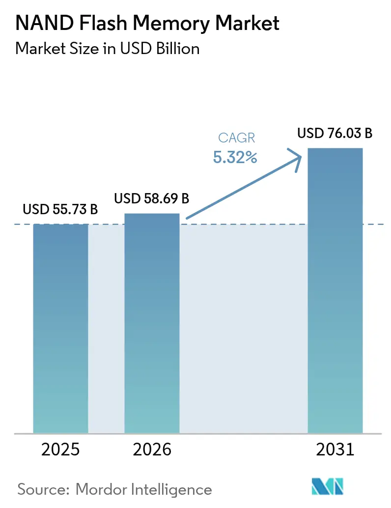
| Market Size (2026) | USD 58.69 Billion |
| Market Size (2031) | USD 76.03 Billion |
| Growth Rate (2026 - 2031) | 5.32% CAGR |
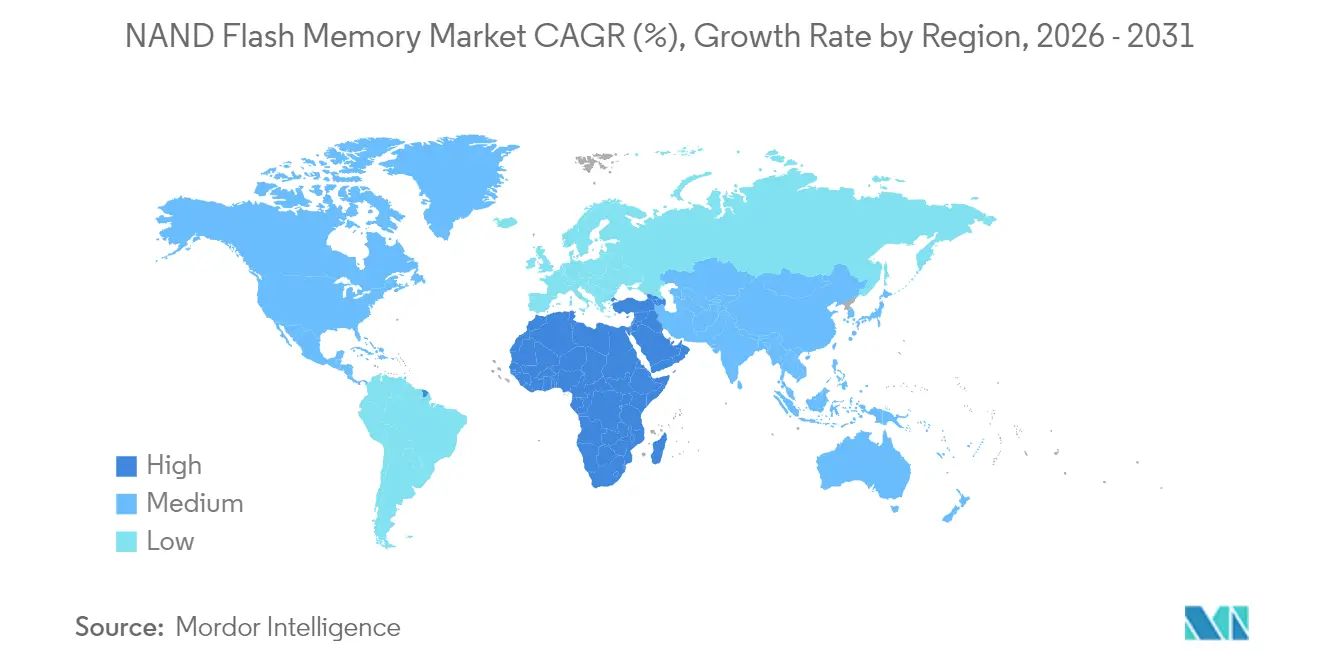
| Fastest Growing Market | Middle East and Africa |
| Largest Market | Asia Pacific |
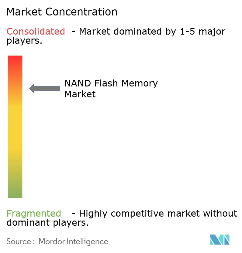
| Market Concentration | High |
Major Players *Disclaimer: Major Players sorted in no particular order Image © Mordor Intelligence. Reuse requires attribution under CC BY 4.0. | |
NAND Flash Memory Market Analysis by Mordor Intelligence
NAND flash memory market size in 2026 is estimated at USD 58.69 billion, growing from 2025 value of USD 55.73 billion with 2031 projections showing USD 76.03 billion, growing at 5.32% CAGR over 2026-2031. This steady expansion is powered by hyperscale data-center capital spending on artificial-intelligence training clusters, the transition of client PCs and game consoles to solid-state storage, and vertically-scaled 3D architectures that keep cost-per-bit on a declining path. At the same time, national incentives to localize semiconductor fabrication, especially in the United States and Saudi Arabia, are strengthening regional supply resilience. Layer-count breakthroughs above 300 layers and PCIe 5.0 adoption are shortening replacement cycles for both enterprise and consumer SSDs. The confluence of 5G rollouts and massive IoT endpoints further widens addressable demand, positioning the NAND flash memory market for durable mid-single-digit growth horizons.
Key Report Takeaways
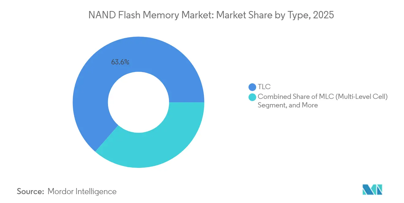
- By type, triple-level cell (TLC) captured 63.58% revenue share of the NAND flash memory market in 2025, whereas quad-level cell (QLC) is projected to expand at 6.35% CAGR through 2031.
- By structure, 3D NAND accounted for 86.85% of the NAND flash memory market size in 2025 and is forecast to grow at a 6.54% CAGR to 2031.
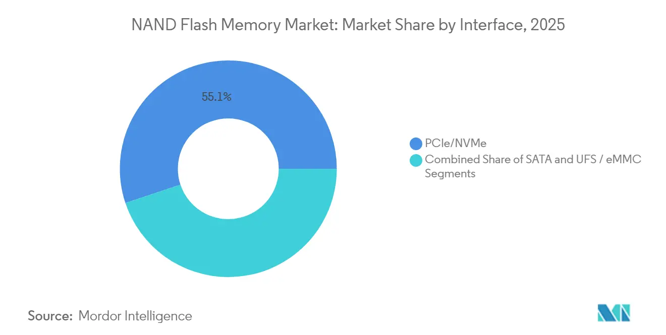
- By interface, PCIe/NVMe commanded 55.12% share of the NAND flash memory market size in 2025, while NVMe-over-PCIe 5.0 is advancing at 7.88% CAGR through 2031.
- By application, smartphones led with 41.05% of the NAND flash memory market share in 2025; enterprise SSDs register the fastest CAGR at 7.42% to 2031.
- By geography, Asia-Pacific held 55.40% of revenue in 2025, whereas the Middle East & Africa region recorded the highest 8.21% CAGR through 2031.
Note: Market size and forecast figures in this report are generated using Mordor Intelligence’s proprietary estimation framework, updated with the latest available data and insights as of 2026.
Global NAND Flash Memory Market Trends and Insights
Drivers Impact Analysis*
| Driver | (~) % Impact on CAGR Forecast | Geographic Relevance | Impact Timeline |
|---|---|---|---|
| Data-center AI/ML storage surge | +1.80% | Global, concentrated in North America and Asia-Pacific | Medium term (2-4 years) |
| 5G and massive-IoT device proliferation | +1.20% | Global, with early adoption in Asia-Pacific and Europe | Long term (≥ 4 years) |
| PC/Console transition from HDD to SSD | +0.90% | Global, led by North America and Europe | Short term (≤ 2 years) |
| Enterprise pivot to cost-efficient QLC SSDs | +0.70% | North America and Europe, expanding to Asia-Pacific | Medium term (2-4 years) |
| National on-shore NAND fab programs | +0.60% | United States, Europe, and select Asia-Pacific countries | Long term (≥ 4 years) |
| CXL-enabled computational storage adoption | +0.40% | North America and Europe data centers | Medium term (2-4 years) |
| Source: Mordor Intelligence | |||


Data-center AI/ML storage surge
Hyperscale operators are redesigning storage hierarchies so that NVMe SSD pools sit closer to GPU clusters, sustaining multi-gigabyte-per-second throughput for retrieval-augmented generation workloads. Western Digital estimates cumulative demand of 19,000 petabytes of NAND by 2029 for 5G-enabled endpoints alone, underscoring flash’s role in bridging memory and cold-storage performance gaps.[1]Western Digital, “Driving AI Innovation: Western Digital Reveals New Solutions and Delivers Keynote at FMS 2024,” Western Digital Blog, Aug 5 2024, westerndigital.com Procurement roadmaps increasingly favor 30 TB to 100 TB enterprise drives, a shift visible in Samsung’s 128 TB BM1743 SSD showcased in 2024. The resulting pull-through effect accelerates layer-count innovation and controller-level compression techniques that sustain the NAND flash memory market momentum.
5G and massive-IoT device proliferation
Standalone 5G deployments unlock edge analytics use cases, smart factories, connected cars, and smart grids that mandate local non-volatile storage for real-time decision engines. Western Digital’s white paper anticipates a NOR-to-NAND crossover within industrial modules as capacities climb above 8 GB.[2]Western Digital, “Driving AI Innovation: Western Digital Reveals New Solutions and Delivers Keynote at FMS 2024,” Western Digital Blog, Aug 5 2024, westerndigital.com Semiconductor roadmaps now prioritize extended-temperature QLC die and automotive-qualified NVMe designs, broadening the NAND flash memory market footprint across transportation and infrastructure domains.
PC/Console transition from HDD to SSD
The consumer PC refresh cycle is synchronized with Microsoft-led minimum spec shifts that disallow HDD-only configurations for Windows 11 installs. In parallel, gaming consoles pivot to NVMe to support real-time texture streaming, as evidenced by Micron’s 3.6 GB/s G9 TLC platform adopted in next-gen devices.[3]Micron Technology, “Micron Announces Volume Production of Ninth-Generation NAND Flash Technology,” Micron Investor Relations, Jul 30 2024, micron.com Cost parity with 2.5-inch HDDs, expected by 2026, removes the last pricing barrier for mass solid-state adoption, giving the NAND flash memory market a predictable volume baseline.
Enterprise pivot to cost-efficient QLC SSDs
Data-lake, log-storage, and content-delivery workloads are 90% read-dominant, an ideal fit for QLC flash. Solidigm benchmarks reveal up to 61% TCO reductions versus TLC-based arrays, driving cloud platforms to roll out ≥ 64 TB QLC eSSDs for AI data-lakes.[4]Solidigm, “QLC NVMe SSDs Are Optimal for Modern Workloads,” Solidigm Technical Brief, Jul 31 2023, solidigm.com Controller advances such as adaptive write-caching reduce write-amplification, mitigating endurance anxiety and widening QLC’s serviceable-available-market inside the NAND flash memory market.
Restraints Impact Analysis*
| Restraint | (~) % Impact on CAGR Forecast | Geographic Relevance | Impact Timeline |
|---|---|---|---|
| Endurance limits of high-density cells | -0.80% | Global, particularly affecting enterprise segments | Medium term (2-4 years) |
| Pricing cyclicality and cap-ex burden | -1.20% | Global, with pronounced effects in Asia-Pacific | Short term (≤ 2 years) |
| Export-control induced equipment bottlenecks | -0.60% | China and allied countries, global supply chain impacts | Long term (≥ 4 years) |
| Sustainability scrutiny on high-layer fabs | -0.40% | Europe and North America, expanding globally | Long term (≥ 4 years) |
| Source: Mordor Intelligence | |||
Endurance limits of high-density cells
QLC’s 1,000–3,000 program/erase thresholds remain insufficient for log-heavy databases, forcing over-provisioning that erodes cost benefits. Hackaday notes the physics ceiling approaching as electron-trap wear accelerates in 300-layer stacks.[5]Hackaday, “The Flash Memory Lifespan Question: Why QLC May Be NAND Flash’s Swan Song,” Hackaday, Jul 8 2024, hackaday.com Although advanced error-correction and wear-leveling algorithms offset degradation, alternate memories such as PLC or cross-point remain on the horizon, tempering portions of the NAND flash memory market until longevity is proven.
Pricing cyclicality and cap-ex burden
Four suppliers control ≈ 95% of global output, giving production cuts outsized influence on spot-pricing. TrendForce recorded a deliberate 50% wafer reduction by Samsung in 2023 to arrest price free-fall; a rebound of more than 50% ensued within months.[6]TrendForce, “Market Anticipates a 50% Price Surge for NAND Flash in Short-Term,” TrendForce News, Dec 29 2023, trendforce.com Yet each greenfield fab now costs beyond USD 10 billion, elongating payback periods and creating capital-intensity headwinds that can slow node-transition investment across the NAND flash memory market.
*Our forecasts treat driver/restraint impacts as directional, not additive. The impact forecasts reflect baseline growth, mix effects, and variable interactions.
Segment Analysis
By Type: QLC challenges TLC dominance
The NAND flash memory market size for TLC devices held a 63.58% market share with the strength of balanced endurance and cost. QLC, however, is accelerating at 6.35% CAGR as hyperscalers validate its 8-16× density advantage for AI data-lakes, which lifts the overall NAND flash memory market share allocated to QLC by 2031. Samsung’s 280-layer QLC prototype signals a roadmap to 16 TB single-sided M.2 drives, shrinking rack footprints while meeting throughput rules for inference clusters. Controller-level SLC-cache techniques and on-die ECC are narrowing the latency gap with TLC, encouraging broader workloads such as VOD libraries and backup repositories to migrate. TLC will retain primacy in write-intensive ERP and OLTP environments where its 10,000-plus cycle rating secures predictable quality-of-service.
In consumer notebooks, TLC’s favorable power profile sustains its install base, but falling QLC cost-per-bit is already pressuring mid-range SKUs. Micron’s sixth-gen QLC exhibits 34% lower read latency than first-gen samples, eroding the perceived performance divide. As firmware-defined endurance mitigation matures, OEMs will likely introduce tiered offerings where high-capacity SKUs employ QLC, while premium lines continue on advanced TLC nodes. This interplay keeps both technologies central to the NAND flash memory market over the forecast horizon.


By Structure: 3D NAND consolidation
The shift from planar to vertical stacking is virtually complete: 3D NAND commanded 86.85% of the NAND flash memory market share in 2025. Layer-count breakthroughs, SK Hynix’s commercial 321-layer TLC and Samsung’s 400-plus-layer V-NAND, signal confident scaling beyond the 500-layer watermark before decade-end. The economic logic is clear; vertical scaling adds capacity without shrinking cell size, sidestepping lithography constraints. 2D NAND survives in niche aerospace and defense modules where ultra-low-latency writes outweigh capacity.
Layer additions do stress interconnect resistance and cell-to-cell interference. To overcome this, Kioxia’s CMOS-bonded-array strategy decouples peripheral circuits, boosting I/O efficiency and improving yield in ultra-tall stacks. Samsung’s exploration of hafnia ferroelectrics for creamy-interface gates pursues a similar aim: maintain threshold-voltage margins even as stack height extends.
By Interface: PCIe/NVMe acceleration
PCIe/NVMe constituted 55.12% of revenue in 2025, upending SATA’s long-held dominance. The upgrade to PCIe 5.0 doubles bi-directional bandwidth, a necessity for AI inference servers where GPU clusters ingest tens of gigabytes per second. Samsung’s 5.6 GT/s I/O die exemplifies how controller-level link speeds keep pace with compute fabric demands. SATA remains cost-effective for Chromebook-class devices, yet most notebook OEMs are phasing in PCIe 4.0 and 5.0 sockets by 2026. Unified flash storage (UFS) and eMMC maintain resonance in smartphones and IoT modules owing to power and board-space constraints. Emerging auto-grade NVMe designs with functional-safety extensions are set to lift automotive penetration, bringing new verticals into the NAND flash memory market.
By Application: Enterprise SSD momentum
Smartphones delivered 41.05% of shipments in 2025, but their annual growth tops out in low single digits as average capacity stabilizes near 256 GB. Conversely, enterprise SSD units are climbing at a 7.42% CAGR through 2031, swelling the NAND flash memory market size contribution from data-center channels. Western Digital’s 64 TB QLC eSSD and Samsung’s 128 TB BM1743 demonstrate the density race shaping hyperscaler racks. Gaming notebooks and consoles bring high-margin growth in the client segment; Microsoft’s DirectStorage API places explicit pressure on sequential write speeds, galvanizing the NVMe upgrade pathway.
Industrial and automotive electronics trail in volume but yield higher ASPs per gigabyte. Phison’s assessment that Level-2+ ADAS stacks need up to 2 TB of on-board flash underscores upside potential. Here, stringent temperature, vibration, and functional-safety qualifications command premium pricing, carving out defensible niches inside the broader NAND flash memory market.
Geography Analysis
Asia-Pacific contributed 55.40% of sales in 2025, anchored by South Korea’s vertically-integrated champions and China’s colossal device assembly base. Samsung’s mass production of 9th-generation V-NAND (286 layers) and SK Hynix’s 321-layer TLC line affirm the region’s technology lead. Beijing’s domestic champion YMTC pushes 232-layer QLC nodes despite export-control constraints, illustrating indigenous capacity expansion that preserves Asia-Pacific’s outsized influence on the NAND flash memory market.
North America sits second on revenue league tables, propelled by cloud capital-expenditure intensity. The CHIPS and Science Act bankrolls Micron’s USD 125 billion state-side megafab roadmap, lifting U.S. advanced-memory self-sufficiency by 2035. Canada contributes controller-IP design talent, while Mexico scales module-level assembly lines under USMCA provisions, together reinforcing regional supply diversification.
Europe registers mid-single-digit share, constrained by limited memory wafer fabrication. Nonetheless, automotive and industrial OEMs in Germany and France generate robust demand for auto-grade NVMe modules. Sustainability directives such as the European Green Deal pivot buyers toward power-efficient PCIe 5.0 SSDs that lower rack energy density, a niche European fabs aim to capture through next-generation 3D NAND nodes with under-3 pJ/bit read energy footprints.
The Middle East and Africa present the highest growth rate at 8.21% CAGR. Saudi Arabia’s Vision 2030 underwrites wafer-to-back-end complexes around Riyadh, while Abu Dhabi’s sovereign investors explore joint-ventures with controller specialists to bootstrap a regional supply chain. Ample renewable-energy pipelines and attractive tax regimes draw packaging partners, setting the stage for localized production that boosts the NAND flash memory market penetration across GCC data hubs.

Competitive Landscape
Market concentration is extreme: the top four vendors commanded major market share of global revenue, enabling scale advantages in lithography investments and controller co-design. Samsung’s high market share stems from early adoption of hybrid-bonded V-NAND that unlocks ≥ 400-layer roadmaps. SK Hynix is increasing its market share by leveraging Three-Plugs etch technology to optimize aspect ratios beyond 300 layers. Western Digital and Kioxia share a flash-foundry alliance that pools wafer output and R&D, although their on-again merger talks face opposition from SK Hynix on antitrust grounds.
Strategic moves now center on interface speed, leadership, and computational storage add-ons. Kioxia and SanDisk’s 4.8 Gb/s Toggle DDR 6.0 interface targets disaggregated GPU memory expansion. Samsung’s work on hafnia ferroelectric channel gates eyes sub-1 V program voltages, trimming both power and write-latency to meet AI inference timetables. Emerging entrants such as YMTC capture niche QLC cloud tenders, but export hurdles limit reach. Controller IP vendors, Silicon Motion, Phison, differentiate via AI-based error-prediction firmware that lifts endurance metrics, enabling ODMs to fine-tune SKUs for distinctive workloads.
NAND Flash Memory Industry Leaders
Samsung Electronics Co., Ltd.
SK hynix Inc.
KIOXIA Holdings Corporation
Western Digital Corporation
Micron Technology, Inc.
- *Disclaimer: Major Players sorted in no particular order

Recent Industry Developments
- June 2025: Kioxia rolled out CD9P Series PCIe 5.0 NVMe SSDs built on 8th-gen BiCS FLASH, pushing sequential reads 60% per watt higher and doubling capacity to 61.44 TB; the strategy tightens alignment with GPU-dense AI servers.
- February 2025: Samsung unveiled 10th-gen V-NAND sporting 400-plus layers at 5.6 GT/s, employing hybrid bonding to future-proof for PCIe 6.0 SSDs and defend premium share in the NAND flash memory market.
- February 2025: Kioxia and SanDisk demonstrated 4.8 Gb/s Toggle DDR 6.0 interface and 332-layer die, a partnership designed to accelerate time-to-market for high-bandwidth flash targeting AI accelerators.


Global NAND Flash Memory Market Report Scope
NAND flash is a kind of non-volatile storage technology that does not require power to retain data. In other words, it is a form of electronically erasable programmable read-only memory (EEPROM). It is programmed, erased, and reprogrammed in large blocks. It's called NAND because, at the circuit level, it's similar to the NAND logic function. The scope of the study covers the market on the basis of the type of NAND and different applications in smartphones, SSD, Memory Cards, and Tablet PC across the world.
The NAND flash memory market is segmented by type (SLC ((one-bit per cell), MLC ((second-bit per cell), and TLC (three-bit per cell), QLC (quad level cell)), structure (2-D structure and 3-D structure), application (smartphones, SSD, memory cards, and tablets), and geography (North America, Europe, Asia Pacific, Latin America, Middle-East and Africa). The market sizes and forecasts are provided in terms of value in USD for all the above segments.
| SLC (Single-Level Cell) |
| MLC (Multi-Level Cell) |
| TLC (Triple-Level Cell) |
| QLC (Quad-Level Cell) |
| 2D (Planar) NAND |
| 3D NAND |
| SATA |
| PCIe / NVMe |
| UFS / eMMC |
| Smartphones |
| Solid-State Drives (PC and Console) |
| Enterprise / Data-center SSD |
| Memory Cards and USB Drives |
| Industrial and Automotive Electronics |
| North America | United States | |
| Canada | ||
| Mexico | ||
| South America | Brazil | |
| Argentina | ||
| Rest of South America | ||
| Europe | Germany | |
| United Kingdom | ||
| France | ||
| Italy | ||
| Spain | ||
| Russia | ||
| Rest of Europe | ||
| Asia-Pacific | China | |
| Japan | ||
| India | ||
| South Korea | ||
| South-East Asia | ||
| Rest of Asia-Pacific | ||
| Middle East and Africa | Middle East | Saudi Arabia |
| United Arab Emirates | ||
| Turkey | ||
| Rest of Middle East | ||
| Africa | South Africa | |
| Nigeria | ||
| Rest of Africa | ||
| By Type | SLC (Single-Level Cell) | ||
| MLC (Multi-Level Cell) | |||
| TLC (Triple-Level Cell) | |||
| QLC (Quad-Level Cell) | |||
| By Structure | 2D (Planar) NAND | ||
| 3D NAND | |||
| By Interface | SATA | ||
| PCIe / NVMe | |||
| UFS / eMMC | |||
| By Application | Smartphones | ||
| Solid-State Drives (PC and Console) | |||
| Enterprise / Data-center SSD | |||
| Memory Cards and USB Drives | |||
| Industrial and Automotive Electronics | |||
| By Geography | North America | United States | |
| Canada | |||
| Mexico | |||
| South America | Brazil | ||
| Argentina | |||
| Rest of South America | |||
| Europe | Germany | ||
| United Kingdom | |||
| France | |||
| Italy | |||
| Spain | |||
| Russia | |||
| Rest of Europe | |||
| Asia-Pacific | China | ||
| Japan | |||
| India | |||
| South Korea | |||
| South-East Asia | |||
| Rest of Asia-Pacific | |||
| Middle East and Africa | Middle East | Saudi Arabia | |
| United Arab Emirates | |||
| Turkey | |||
| Rest of Middle East | |||
| Africa | South Africa | ||
| Nigeria | |||
| Rest of Africa | |||


Key Questions Answered in the Report
How large is global demand for flash in AI data-centers by 2031?
Western Digital estimates cumulative consumption of about 19,000 petabytes, with enterprise SSD capacities moving toward the 100 TB class.
When will PCIe 5.0 SSDs become mainstream in notebooks?
OEM shipment roadmaps indicate most premium and mid-range laptops will standardize on PCIe 5.0 by 2026 as controller costs fall.
What share of shipments will QLC devices capture by 2031?
Forecasts in this report show QLC approaching one-fifth of total bits shipped, driven by hyperscale data-lake and archival workloads.
Which region is growing the fastest for memory-fab investment?
The Middle East and Africa, especially Saudi Arabia's Vision 2030 program, leads with an 8.21% CAGR to 2031.
How many layers can current 3D NAND process nodes reliably reach?
Commercial products are at 321-layers, and R&D samples have crossed the 400-layer threshold, setting a trajectory toward 1,000-layers before 2031.
Page last updated on:


