
Japan Semiconductor Device Market Size and Share
Market Overview
| Study Period | 2020 - 2031 |
|---|---|
| Forecast Data Period | 2026 - 2031 |
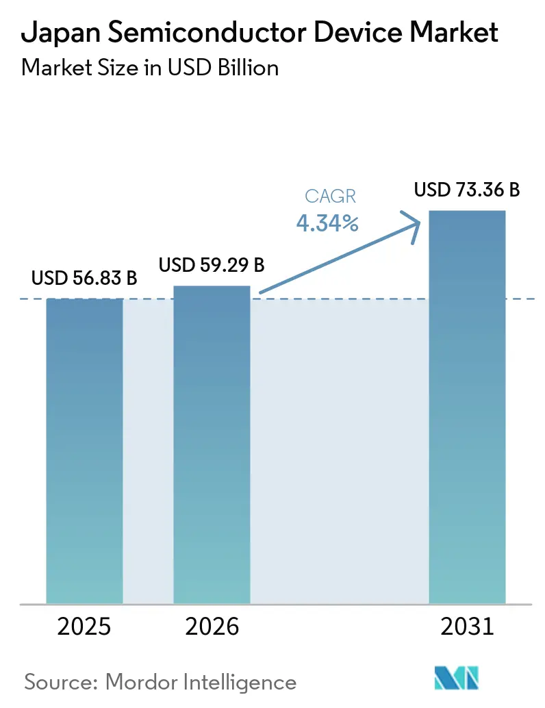
| Base Year Market Size (2025) | USD 56.83 Billion |
| Market Size (2026) | USD 59.29 Billion |
| Market Size (2031) | USD 73.36 Billion |
| Growth Rate (2026 - 2031) | 4.34 % |
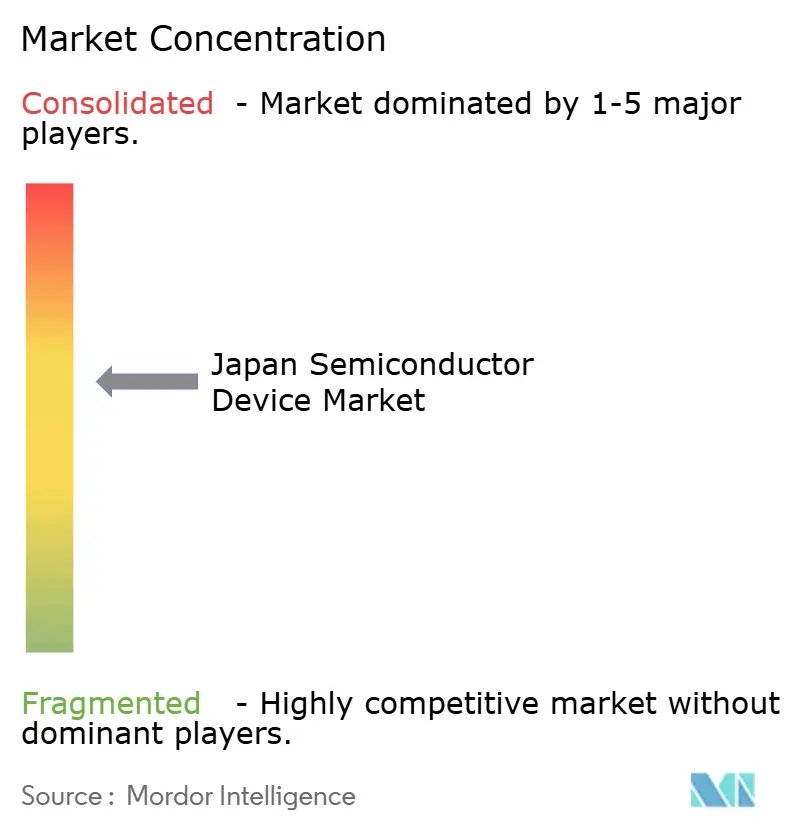
| Market Concentration | Medium |
Major Players *Disclaimer: Major Players sorted in no particular order Image © Mordor Intelligence. Reuse requires attribution under CC BY 4.0. | |
Japan Semiconductor Device Market Analysis by Mordor Intelligence
Japan semiconductor device market size in 2026 is estimated at USD 59.29 billion, growing from 2025 value of USD 56.83 billion with 2031 projections showing USD 73.36 billion, growing at 4.34% CAGR over 2026-2031. Persistent public-sector funding worth JPY 4 trillion during 2021-2023 has moved capital toward advanced materials, EUV-lithography tools, and compound substrates, ensuring that each yen spent yields higher value per wafer. As a result, the Japan semiconductor device market increasingly monetizes intellectual property and equipment know-how rather than commodity output, a shift that insulates revenue from the pricing swings common in global DRAM and logic foundry trades. Expanding clusters in Kumamoto, Hokkaido, and the northeast “Silicon Road” region shorten supply chains, attract foreign direct investment, and reduce logistic risk; these hubs are quickly becoming indispensable nodes for global fabless designers seeking diversification. At the same time, tighter national security regulations and export-control measures widen entry barriers, enabling premium pricing for specialty devices such as SiC MOSFETs, GaN RF amplifiers, and next-generation 3D NAND.
Key Report Takeaways
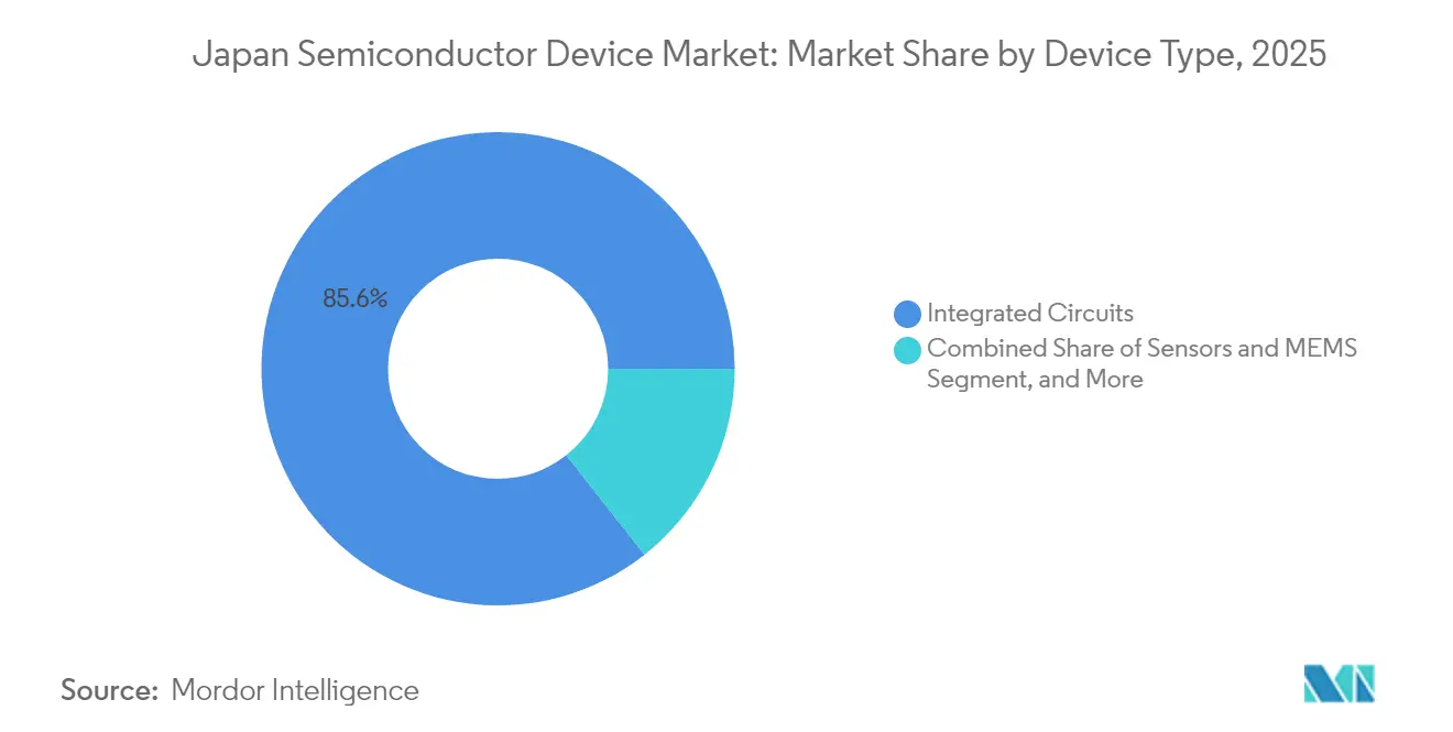
- By device type, Integrated Circuits captured 85.62% of Japan semiconductor device market share in 2025; Sensors and MEMS is on track for a 5.59% CAGR through 2031.
- By business model, IDMs accounted for 72.15% of Japan semiconductor device market share in 2025, while fabless/design houses are projected to expand at a 5.34% CAGR to 2031.
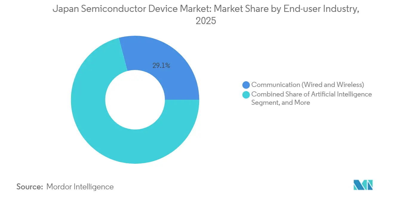
- By end-user industry, Communication led revenue with 29.10% in 2025 of Japan semiconductor device market share, and Artificial Intelligence workloads are forecast to post the fastest 5.95% CAGR to 2031.
Note: Market size and forecast figures in this report are generated using Mordor Intelligence’s proprietary estimation framework, updated with the latest available data and insights as of 2026.
Competitive positioning in Japan includes both locally based firms and those operating across multiple regions. The market landscape in the global semiconductor device industry research shows how these players are arranged internationally.
Japan Semiconductor Device Market Trends and Insights
Drivers Impact Analysis*
| Driver | (~) % Impact on CAGR Forecast | Geographic Relevance | Impact Timeline |
|---|---|---|---|
| EV power-train demand surge | +1.2% | National automotive corridors | Medium term (2-4 years) |
| Robust 5G/6G roll-out | +0.9% | Major urban centers nationwide | Short term (≤ 2 years) |
| Government subsidies for advanced-node fabs | +0.8% | Kumamoto and Hokkaido | Long term (≥ 4 years) |
| Consumer IoT proliferation in smart homes | +0.6% | Metropolitan regions | Medium term (2-4 years) |
| Vertical GaN/SiC R&D leadership | +0.5% | National research hubs | Long term (≥ 4 years) |
| Reshoring incentives for secure supply chains | +0.4% | Strategic fab locations nationwide | Long term (≥ 4 years) |
| Source: Mordor Intelligence | |||
Electric-vehicle power-train demand surge
EV architectures replace multiple mechanical parts with solid-state subsystems, elevating demand for traction inverters, on-board chargers, and ADAS controllers. Domestic leaders deploy d-mode GaN switches that outperform SiC at mid-range voltages, broadening addressable markets while retaining pricing power. Strategic partnerships between tier-one suppliers and device makers accelerate design-win cycles, ensuring that the Japan semiconductor device market benefits from higher silicon content per vehicle.[1]“Mitsubishi Electric to Ship Samples of XB Series HVIGBT Module,” Mitsubishi Electric Corporation, mitsubishielectric.com Mandatory carbon-reduction targets solidify local offtake agreements, and a deep automotive ecosystem supports rapid qualification, embedding power-device gains for the medium term.
Robust 5G/6G infrastructure roll-out
Japan’s mid-band densification and pre-standard 6G testbeds push throughput and latency specifications that legacy silicon cannot satisfy. Domestic RF specialists combine GaN HEMTs with proprietary matching networks to hit base-station thermal limits, cementing share while capturing premium margins. Localization of plasma-etch and MOCVD tool supply further lowers production risk, drawing additional foreign fabless orders into the Japan semiconductor device market cluster. Spillovers into network-testing equipment widen downstream opportunities, guaranteeing sustained incremental demand.
Government subsidies for advanced-node fabs
Unlike direct capacity grants seen elsewhere, Japan ties relief to technology-transfer metrics and tax deductions linked to sustained local output. This design nurtures a vertically integrated ecosystem spanning photoresist chemistries, EUV pellicles, and advanced packaging, preserving sovereign control. The approach raises switching costs for multinationals, who locate R&D modules onshore to retain eligibility. These measures ensure that the Japan semiconductor device market commands long-term comparative advantages in both leading-edge and specialty nodes.
Consumer IoT proliferation in smart homes
Labor scarcity and an aging population heighten interest in home automation and ambient-assisted living devices that depend on low-power MCUs, MEMS microphones, and radar sensors. Energy-efficiency subsidies accelerate uptake of smart-metering systems, funneling stable orders to domestic fabs comfortable with mixed-signal processes. Cross-pollination of industrial-robotics know-how into consumer form factors differentiates Japanese suppliers in a crowded IoT landscape, lifting volume without diluting margins.
Restraints Impact Analysis*
| Restraint | (~) % Impact on CAGR Forecast | Geographic Relevance | Impact Timeline |
|---|---|---|---|
| Chronic talent shortage in advanced lithography | -0.8% | All advanced-node regions | Medium term (2-4 years) |
| Supply-chain exposure to specialty gases and chemicals | -0.6% | Nation-wide advanced fabs | Short term (≤ 2 years) |
| Earthquake-induced downtime risk for fabs | -0.4% | Seismically active coastal zones | Long term (≥ 4 years) |
| Legacy equipment obsolescence for sub-28 nm nodes | -0.3% | Older fabrication facilities | Medium term (2-4 years) |
| Source: Mordor Intelligence | |||
Chronic talent shortage in advanced lithography
EUV tool installations require engineers versed in sub-2 nm process integration, yet the domestic pipeline adds only a few dozen graduates per year. Multinationals lure experienced staff overseas with double-digit wage premiums, widening local gaps. Although scholarship programs and mid-career retraining provide relief, ramp schedules still hinge on expatriate hires, stretching learning curves and raising risk of yield-ramp delays that could dent the Japan semiconductor device market’s near-term growth trajectory.
Supply-chain exposure to specialty gases and chemicals
High-purity hydrogen fluoride, gallium, and germanium remain vulnerable to geopolitical curbs. Domestic chemical giants launched multi-year capex plans, but ISO-14644 compliance and tier-one customer audits take time, slowing full localization. Short-notice disruptions force fabs to idle lines or expedite small-lot imports, eroding wafer-level margins. Until replacement capacity matures, chemical dependency will continue to clip the upper bound of annual output growth.
*Our forecasts treat driver/restraint impacts as directional, not additive. The impact forecasts reflect baseline growth, mix effects, and variable interactions.
Segment Analysis
By Device Type: Integrated Circuits Drive Market Value
Integrated Circuits generated 85.62% of Japan semiconductor device market revenue in 2025, sustained by bespoke AI accelerators, automotive SoCs, and multilayer 3D NAND. Edge-inference ASICs consume leading-edge wafers, while high-layer NAND packages fill cloud-storage racks, anchoring volume in separate but complementary streams. Sensors and MEMS, though smaller, expand at a 5.59% CAGR as ADAS radar and factory-floor retrofits multiply attach points. Optoelectronics leverages national leadership in laser diodes for LiDAR and AR headsets. In the Japan semiconductor diode market, Pulsed laser diodes are used in amplitude-modulated LiDAR systems for automotive applications. Discrete power devices grow modestly, but SiC MOSFETs and GaN transistors earn richer ASPs, stabilizing contribution margins.
A node-level view highlights a dual-track approach: sub-7 nm lines support AI and high-performance computing, whereas mature 40-65 nm flows serve car electronics and industrial control. This split lets the Japan semiconductor device market capture demand across cycles, underwriting balanced fabs that avoid over-reliance on any single customer vertical. Breakthroughs such as 1,000-layer 3D NAND will keep density leadership in the domestic ecosystem, strengthening export competitiveness.



By Business Model: IDM Dominance Faces Fabless Pressure
IDMs delivered 72.15% of revenue in 2025 because vertical integration secures material supply and process IP. Control over epitaxial reactors, CMP slurries, and back-end test lines enables tighter design-to-device loops, a critical edge for safety-certified automotive ICs.
Nonetheless, fabless entrants scale at 5.34% CAGR, encouraged by new foundry capacity in Kumamoto and Chitose. Domestic IDMs respond by offloading legacy nodes to specialty foundries, channeling captive clean-room space toward SiC and EUV experiments. This hybridization boosts return on invested capital, keeping the Japan semiconductor device market agile while preserving core know-how behind corporate firewalls.
By End-user Industry: Communication Leadership Shifts to AI
Communication infrastructure, including 5G macro cells and optical-transport gear, held 29.10% of Japan's semiconductor device market revenue in 2025. Carrier densification requires RF filters and duplexers built on GaN or advanced ceramic substrates, lines where Japanese suppliers dominate.
Meanwhile, Artificial Intelligence captures the highest 5.95% CAGR as hyperscale data centers and sovereign AI clusters push petaflop budgets skyward. Memory-bandwidth requirements propel high-layer NAND shipments; proprietary controller ICs lock in ecosystem stickiness. Automotive electronics maintain mid-single-digit growth, cushioned by stringent safety mandates, while industrial robotics sustains steady momentum through continuous factory-automation upgrades.
Geography Analysis
Kumamoto Prefecture emerged as the flagship node of the Japan semiconductor device market after landmark subsidies drew TSMC’s JASM foundry and dozens of ancillaries. Commercial land prices climbed more than 10% in 2024 amid supplier inflows, confirming the cluster’s economic gravity. JASM’s advanced logic output couples with Sony’s long-standing image-sensor expertise, forging a full-stack corridor from wafer etch to camera module assembly. Proximity of compressor, gas, and DI-water vendors trims downtime, stabilizing yields.
Hokkaido’s “Chip Valley” adopts a research-heavy blueprint anchored by Rapidus’s 2 nm pilot line. Abundant hydroelectric capacity lowers per-wafer electricity cost, meeting green-procurement criteria set by global hyperscalers. Collaboration between local universities and equipment makers accelerates EUV metrology breakthroughs, cementing long-term relevance even before mass production scales. Government zoning reforms streamline land acquisition, and public-sector dormitories ease relocation for specialized engineers, gradually narrowing the lithography talent gap.
The historic northeast “Silicon Road” regains momentum as equipment leader Tokyo Electron adds etch-tool capacity and upstream suppliers revamp lines for high-aspect-ratio vias. Mid-tier OSAT firms piggy-back on these upgrades, forming a spoke-and-hub service mesh that shortens logistics cycles between wafer output in Kumamoto and package final-test facilities. Together, these regional strategies diversify seismic risk, localize critical inputs, and solidify the Japan semiconductor device market as an all-in-one ecosystem.
Mordor Intelligence tracks the semiconductor device market across other major regions such as Asia and Europe, with additional country-level coverage spanning South Korea and China, each reflecting localized structural drivers, restraints and more.
Regulatory Landscape
Japan is tightening oversight while also using industrial policy to build domestic semiconductor capacity. The Act on the Promotion of Ensuring National Security Through Integrated Implementation of Economic Measures (Economic Security Promotion Act) underpins the designation of semiconductors as specified critical materials and provides support measures aimed at strengthening supply assurance. METI also runs an Early Warning Alert Mechanism for semiconductor supply chain disruptions (established in December 2023), which adds a formal monitoring layer that shapes procurement, inventory, and continuity planning across fabs and downstream device makers.
On trade and cross-border technology governance, Japan has strengthened export-control measures around advanced semiconductor and quantum-related technologies (with amendments referenced in 2025 within the report context), increasing compliance demands for firms handling leading-edge process know-how and related design IP. METI has also pursued international coordination, including a semiconductor Memorandum of Cooperation with the European Commission (July 2023). Policy channels such as METI-linked programs, including IPA-related support mechanisms, continue to mobilize project support and capital toward strategic device categories and enabling technologies.
Value Chain Analysis
Japan semiconductor devices move through an integrated value chain that spans materials and equipment, wafer fabrication, assembly and test, and end-market system integration, with clustering in regions such as Kumamoto and Hokkaido reducing logistics and qualification friction. Upstream depth in chemicals, substrates, photoresists, and equipment supports both leading-edge and specialty manufacturing, while national security-driven measures, including METI supply-chain monitoring via the December 2023 early-warning mechanism, push OEMs and fabs to map tier-n suppliers, qualify alternates, and localize critical inputs where feasible.
Midstream dynamics increasingly reflect specialization and selective consolidation, particularly in power semiconductors used in automotive electrification and AI infrastructure power delivery. Reported negotiations involving Mitsubishi Electric, Rohm, and Toshiba around integrating parts of their power semiconductor operations point to a shift toward scale and broader portfolios across SiC MOSFETs, IGBT modules, and silicon MOSFET/IGBT lines, with knock-on effects for wafer sourcing, module packaging, and customer qualification. Downstream, device makers and IDMs are extending value capture beyond silicon by bundling application software and system solutions, illustrated by Renesas expanding embedded and vision-AI software capabilities through acquisitions, while product roadmaps increasingly emphasize packaging and thermal performance to meet data center, base-station, and xEV requirements.
Competitive Landscape
The Japan semiconductor device market shows moderate concentration; top materials, equipment, and device firms jointly command slightly above 60% of the segment revenues, giving them leverage without stifling innovation by mid-tier specialists. Tokyo Electron remains indispensable for plasma etch gear in sub-5 nm flows, shipping multi-chamber modules that balance throughput and defectivity. Shin-Etsu’s dominance in photoresist and immersion fluids constrains rival fab suppliers, reinforcing stickiness among EUV customers.[3]“Japan Back-End Chip Companies Form Alliance,” Nikkei Asia, asia.nikkei.com Renesas bends design roadmaps toward EV inverters, while Rohm’s vertically integrated SiC supply captures extra die value.
Corporate strategy leans toward alliances rather than outright M&A, limiting integration risk. Mitsubishi Electric’s USD 500 million SiC-substrate joint venture exemplifies targeted vertical moves that lock in scarce inputs without ballooning capex. Diamond-semiconductor consortia blend academic patents with SME process expertise, seeding options beyond SiC and GaN for extreme-temperature electronics. Export-control amendments enacted in 2025 restrict the outbound transfer of quantum and advanced-node IP, erecting regulatory moats around domestic technology. Cumulative patent-issuance data show Japanese entities are responsible for over one-third of GaN power-device grants since 2023, underscoring defensible technological depth.
Japan Semiconductor Device Industry Leaders
Renesas Electronics Corporation
Rohm Co., Ltd.
Toshiba Electronic Devices and Storage Corporation
Sony Semiconductor Solutions Corporation
Kioxia Holdings Corporation
- *Disclaimer: Major Players sorted in no particular order

Market Opportunities and Future Outlook
Public policy and funded manufacturing programs are creating whitespace for suppliers that can meet domestic content, security, and performance requirements across logic, memory, and power devices. Japan has articulated an industrial ambition to reach JPY 40 trillion in sales of domestically produced semiconductors by 2040, and METI has indicated increased funding focus for advanced semiconductors and AI from April 2026. This reinforces multi-year program visibility for device makers, materials suppliers, and equipment vendors working on advanced-node capabilities, advanced packaging, and AI-adjacent components.
Nearer-term opportunities concentrate on (i) power semiconductors for xEVs and data center power conversion, and (ii) photonics-electronics convergence manufacturing lines that extend beyond conventional CMOS scaling. Company actions support these demand pockets: Toshiba introduced U-MOS11-H process-based 80V N-channel power MOSFETs in June 2026 for AI data center and communications power supplies, while Rohm moved on both packaging and device roadmaps with mass production of a top-side cooling package for SiC MOSFETs (June 2026) and new 600V super junction MOSFETs (July 2026). On capacity and technology platforms, METI-backed subsidies for Tower Semiconductor Japan G.K. (up to JPY 160 billion) for photonics-electronics convergence devices in Toyama and Niigata, with production planned to start in May 2027, provide a tangible route for Japan-based output in emerging device architectures and supply-chain localization requirements.
Recent Industry Developments
- July 2026: ROHM Semiconductor launches 600V Super Junction MOSFETs in surface-mount package with high thermal performance. The rollout targets high-efficiency power devices for AI data centers and automotive power, expanding ROHM's footprint in critical markets. Packaging-focused expansion addresses thermal and space constraints to support dense, high-power designs.
- July 2026: Renesas Electronics Corporation completes transfer of timing business to SiTime Corporation. The shift impacts embedded timing components and designs for RS/MCU ecosystems, enabling a streamlined product roadmap. Consolidating timing capability accelerates time-to-market and reduces development risk for customers.
- June 2026: ROHM Semiconductor mass production of TSC3PAK package for SiC MOSFETs to improve heat dissipation in xEV applications. This packaging optimization strengthens ROHM's position in high-efficiency power electronics and the EV supply chain. The advance supports broader adoption of SiC based power solutions in next generation electric vehicles.


Research Methodology Framework and Report Scope
Market Definition and Coverage
For this methodology, the Japan semiconductor device market is measured as the value of semiconductor devices sold for use in Japan across major device categories, captured in USD at current prices.
Scope exclusions: We do not count semiconductor manufacturing equipment, materials, or wafer fabrication services as market revenue.
Segmentation Overview
- By Device Type
- Discrete Semiconductors
- Diodes
- Transistors
- Power Transistors
- Rectifier and Thyristor
- Other Discrete Semiconductors
- Optoelectronics
- Light-Emitting Diodes (LEDs)
- Laser Diodes
- Image Sensors
- Optocouplers
- Other Optoelectronics
- Sensors and MEMS
- Pressure
- Magnetic Field
- Actuators
- Acceleration and Yaw Rate
- Temperature and Other Sensors and MEMS
- Integrated Circuits
- By IC Type
- Analog
- Micro
- Microprocessors (MPU)
- Microcontrollers (MCU)
- Digital Signal Processors
- Logic
- Memory
- By Technology Node
- less than 3 nm
- 3 nm
- 5 nm
- 7 nm
- 16 nm
- 28 nm
- Above 28 nm
- By IC Type
- Discrete Semiconductors
- By Business Model
- IDM
- Design/Fabless Vendor
- By End-user Industry
- Automotive
- Communication (Wired and Wireless)
- Consumer
- Industrial
- Computing/Data Storage
- Data Centre
- Artificial Intelligence
- Government (Aerospace and Defence)
- Other End-user Industry
Data Sources, Market Sizing, and Validation
Desk Research
Desk work starts by aligning the scope to Japan device demand signals, and then mapping the key series that can be tracked consistently year after year. Public statistical releases are used to anchor the direction of production and shipments, and to sense-check the timing of upcycles and downcycles.
The main references include official and industry sources such as Japan customs trade statistics for electronics-related imports and exports, METI production and shipment indices, JEITA electronics and electronic components statistics, and WSTS country level semiconductor market tables that are frequently reused by policymakers. We also review company filings, investor presentations, and credible business press to understand mix shifts like automotive power devices, sensors, and memory, and then cross-check specific points using paid subscriptions focused on company financials, patent databases, and shipment-level import and export data. This desk source list is illustrative and not exhaustive, since many other documents are checked to collect data, validate it, and clarify open questions.
Primary Interviews and Surveys
Primary work is used to confirm what the desk sources cannot show cleanly, such as current pricing behavior, channel inventory pressure, and the practical split between device categories that are shipped into Japan versus produced locally. We interview and survey a mix of device makers, distributors, OEM buying teams, and industry experts so our assumptions on volumes, ASP movements, and end-use demand are corrected before the model is finalized.
Distribution of primary research fieldwork respondents
| Company type | Respondent position |
|---|---|
| Top tier: 31% | CXOs: 12% |
| Mid tier: 55% | Functional/Unit leaders: 30% |
| Smaller Players: 14% | Managers: 58% |
Market-Sizing & Forecasting
The sizing logic starts with a top-down build where Japan device demand is reconstructed from country level semiconductor consumption signals, production and shipment direction, and the device mix seen across the main end markets. Once the demand pool is formed, it is translated into value using category level ASP indicators, followed by adjustments for currency timing and known inventory swings.
To keep the numbers grounded, the totals are corroborated through selective bottom-up checks, such as sampled ASP multiplied by estimated unit volumes for high impact device groups and distributor channel checks for near term corrections. Inputs that matter most in this market include the split between integrated circuits and discrete devices, the share of automotive and industrial demand (especially power and sensor content), factory utilization and output trends reported in Japan industry statistics, import and export flows for electronics components, and the cadence of memory pricing cycles that can move market value even when units are stable.
For forecasting, we rely on scenario analysis supported by time series smoothing on the historical baseline, and then we apply primary feedback to tune the forward path for end market production, AI server related demand, and planned capacity and investment changes. Where bottom-up evidence is thin for a niche device group, we bridge the gap with ratio based allocation from the closest reported device family and then re-check the implied growth rate against independent production and trade indicators.
Data Validation & Update Cycle
Outputs are validated in several passes so obvious errors do not slip through. We compare modeled market totals against independent signals like country level semiconductor consumption tables, domestic production and shipment direction, and the implied import dependence, and then review any sharp variance at the device family level.
If an anomaly looks material, assumptions are revisited and targeted re-contacts are triggered with primary respondents to confirm whether the change is real or simply timing related. Before sign-off, another analyst reviews the logic, math, and reasonableness of growth and mix, and a final pre-delivery check is completed so the latest public updates and major events are reflected. The report is refreshed annually, with interim updates made when major market events or policy actions materially change the outlook.
Mordor Intelligence's Japan Semiconductor Device Market Size Compared Against Other Published Estimates
Published market values for Japan semiconductors often do not line up because different authors mix device scope, geography rules, and the way they treat pricing cycles and currency timing. Some estimates are also released on a different refresh schedule, so the same year can still reflect different information cutoffs.
A common difference is that broader figures are sometimes presented as a single semiconductor total and may be closer to an overall consumption view, which can blur device categories and occasionally mix in adjacent electronics value. In contrast, Mordor Intelligence counts semiconductor devices sold into Japan and keeps the model tied to device families and end-use demand checks, which helps avoid accidental inclusion of equipment or other non-device revenue.
Benchmark comparison
| Source | Market Size | Gaps in Research Methodology |
|---|---|---|
| Mordor Intelligence | USD 56.83 B (2025) | |
| Government Trade Brief A | USD 51.89 B (2025) | Uses a country level semiconductor market table that can behave like a total consumption view, and it may not separate device families or adjust for near term inventory and ASP swings the same way. |
| Industry Portal B | USD 50.29 B (2024) | Reported year differs and the scope is often summarized without clear inclusion rules for optoelectronics, sensors, and discrete categories, which can shift totals when mix changes across automotive and industrial demand. |
The table shows that the spread is explained mostly by scope and timing, followed by how pricing cycles and currency conversion are applied. By keeping the inputs traceable to device categories, end-market demand, and cross-checkable external signals, the final estimate stays repeatable and easier to reconcile when the market turns.


Key Questions Answered in the Report
How big is the Japan semiconductor market in 2026?
It is valued at USD 59.29 billion and is forecast to grow to USD 73.36 billion by 2031 at a 4.34% CAGR.
Which device category leads revenue contribution?
Integrated Circuits dominate with 85.62% share in 2025, driven by AI accelerators and high-layer 3D NAND.
Which application segment is expanding fastest?
Artificial Intelligence applications post the highest 5.95% CAGR through 2031 on the back of hyperscale data-center buildouts.
Where are the main semiconductor hubs located?
Kumamoto anchors new logic foundries, Hokkaido hosts 2 nm R&D lines, and the northeast “Silicon Road” concentrates equipment suppliers.
What is the primary growth driver for power devices?
EV electrification spurs demand for SiC and GaN components used in traction inverters and on-board chargers.
What regulatory factor shapes competitive dynamics?
Export-control extensions implemented in 2025 restrict outbound transfer of advanced-node and quantum-computing IP, reinforcing domestic barriers.
Page last updated on:


 Your data is secure and never sold or shared.


