Die Bonder Equipment Market Size and Share
Market Overview
| Study Period | 2020 - 2031 |
|---|---|
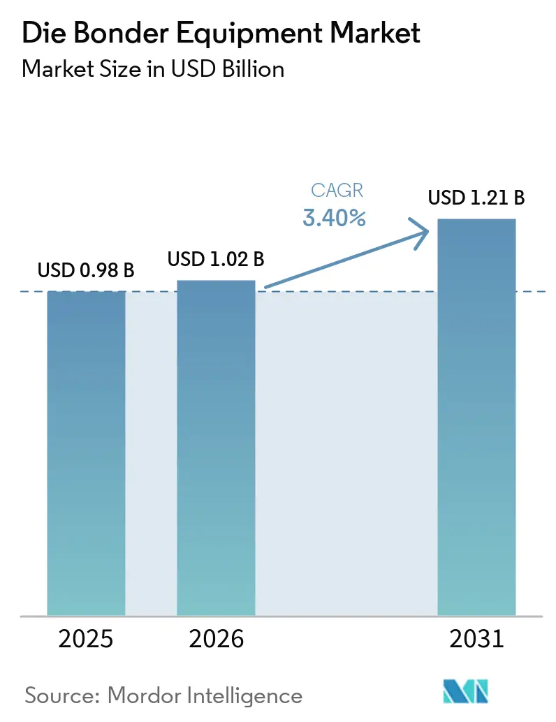
| Market Size (2026) | USD 1.02 Billion |
| Market Size (2031) | USD 1.21 Billion |
| Growth Rate (2026 - 2031) | 3.40% CAGR |
| Fastest Growing Market | Middle East |
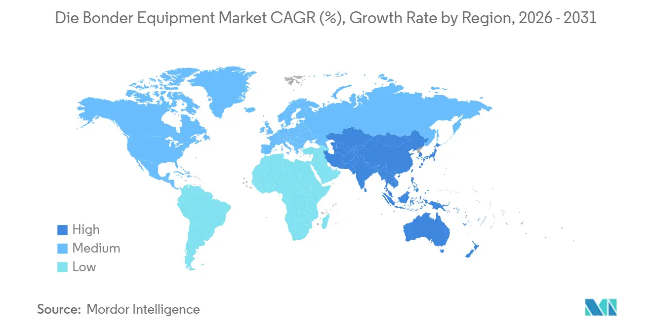
| Largest Market | Asia Pacific |
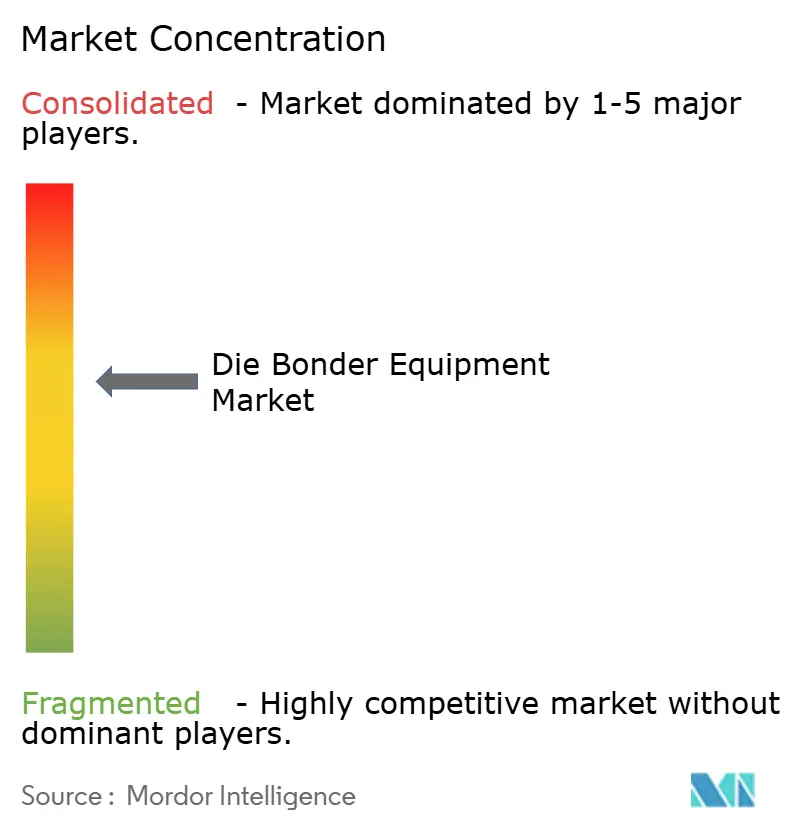
| Market Concentration | Medium |
Major Players
*Disclaimer: Major Players sorted in no particular order Image © Mordor Intelligence. Reuse requires attribution under CC BY 4.0. |
|
Die Bonder Equipment Market Analysis by Mordor Intelligence
The Die Bonder Equipment Market size is expected to increase from USD 0.98 billion in 2025 to USD 1.02 billion in 2026 and reach USD 1.21 billion by 2031, growing at a CAGR of 3.40% over 2026-2031.
Market participants are re-tooling capacity for sub-micron accuracy as chiplet economics and high-bandwidth memory demand hybrid, thermocompression, and wafer-to-wafer bonding platforms. Capital spending is gravitating toward fully automatic machines that integrate vision systems, inline metrology, and process-control software to guarantee first-pass yields above 99.5%. Equipment with real-time force-feedback and active thermal compensation is becoming standard because silicon, compound-semiconductor, and organic substrates move at different coefficients of thermal expansion. Procurement cycles are lengthening to 12-18 months for motion-control stages and high-resolution vision modules, creating temporary supply imbalances that favour suppliers with vertically integrated manufacturing.
Key Report Takeaways
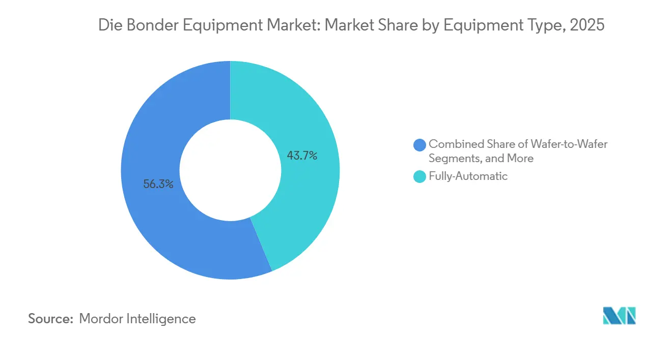
- By equipment type, fully automatic machines led with 43.74% revenue share in 2025, while wafer-to-wafer bonders are projected to grow at a 3.91% CAGR through 2031.
- By bonding technology, flip-chip platforms accounted for 32.38% of die bonder equipment market share in 2025; hybrid and direct Cu-Cu bonding are forecast to expand at a 4.14% CAGR to 2031.
- By throughput category, high-speed tools above 60,000 UPH captured 38.63% of 2025 revenue, whereas low-speed, high-precision systems below 30,000 UPH will advance at a 4.23% CAGR during 2026-2031.
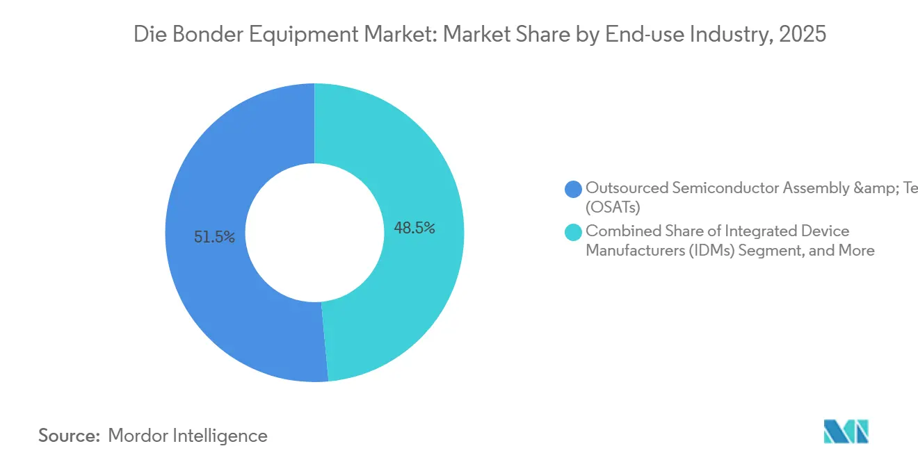
- By end-use industry, outsourced semiconductor assembly and test providers held 46.58% of 2025 demand; photonics research labs represent the fastest-growing customer group at a 4.06% CAGR.
- By device type, logic and memory integrated circuits dominated with a 40.73% revenue share in 2025, yet photonics and optical transceivers are set to grow at a 3.98% CAGR to 2031.
- By geography, Asia-Pacific accounted for accounted for the largest revenue share with 55.88% in 2025, however Middle East is expected to growa at the fastest rate with 4.11% CAGR to 2031.
Note: Market size and forecast figures in this report are generated using Mordor Intelligence’s proprietary estimation framework, updated with the latest available data and insights as of January 2026.
Global Die Bonder Equipment Market Trends and Insights
Drivers Impact Analysis*
| Driver | (~) % Impact on CAGR Forecast | Geographic Relevance | Impact Timeline |
|---|---|---|---|
| Heterogeneous-Integration and Chiplet Boom | +0.9% | Global, with APAC and North America leading adoption | Medium term (2-4 years) |
| Advanced 2.5D/3D and Hybrid Bonding Adoption | +0.8% | APAC core, spill-over to North America and Europe | Long term (≥ 4 years) |
| Rapid Uptake of Compound-Semiconductor Power Devices | +0.6% | Global, with strong traction in Europe and North America automotive hubs | Short term (≤ 2 years) |
| Data-Center Photonics and Co-Packaged Optics Demand | +0.5% | North America and APAC data-center clusters | Medium term (2-4 years) |
| Government On-Shoring Subsidies for Back-End Fabs | +0.3% | United States, European Union, India, with secondary effects in Middle East | Short term (≤ 2 years) |
| Industry 4.0 Push for Fully-Automatic High-UPH Bonders | +0.2% | APAC manufacturing corridors, expanding to emerging markets | Long term (≥ 4 years) |
| Source: Mordor Intelligence | |||
Heterogeneous-Integration and Chiplet Boom
Chiplet partitioning breaks monolithic system-on-chip designs into smaller tiles connected by fine-pitch die-to-die links, slashing reticle cost and improving yield while demanding placement accuracy tighter than 2 µm. Early high-volume shipments of chiplet CPUs validated the economics and triggered a shift from wire bonding toward thermocompression platforms that process one bond instead of dozens of wires, raising tool utilization and justifying higher capital outlays.[1]Intel Corporation, “Intel Advances Moore’s Law with Foveros 3D Packaging Technology,” intel.com Universal Chiplet Interconnect Express is standardizing protocols, making advanced packaging accessible to second-tier device makers and expanding the die bonder equipment market. Suppliers are responding with dual-gantry systems, interferometric sensors, and machine-learning alignment engines that cut setup time and improve first-pass yield. The payoff for customers is a mix-and-match design flow that extends Moore’s Law economically even as front-end scaling slows.[2]AMD Inc., “AMD EPYC and Ryzen Processors Leverage Chiplet Architecture,” amd.com
Advanced 2.5D 3D And Hybrid Bonding Adoption
Hybrid bonding fuses copper pads and dielectric layers at around 200 °C, eliminating microbumps and lifting connection density above 10,000 links mm-2, a prerequisite for next-generation high-bandwidth memory and graphics accelerators. Tool vendors are co-optimizing wafer-to-wafer bonders with planarization steps to keep copper dishing below 5 nm and overlay error under 200 nm. Nanotwinned copper is widening the thermal process window, making organic substrates viable for fine-pitch 3D stacking. Because hybrid-bonding lines cost 50-70% more than flip-chip lines, adoption is initially concentrated at top-tier IDMs and OSATs that can amortize multi-million-dollar tool sets across high-volume programs. Once HBM generation 5 ramps after 2028, a material replacement wave will cascade through memory and logic supply chains, accelerating demand for hybrid-ready die bonders.[3]Samsung Electronics, “High Bandwidth Memory Roadmap and Hybrid Bonding Technology,” samsung.com
Rapid Uptake of Compound-Semiconductor Power Devices
Electric-vehicle inverters and industrial drives are shifting to silicon carbide and gallium nitride switches that operate at higher frequencies and temperatures, delivering system-level efficiency gains of 5-8%. These wide-bandgap chips require silver-sintered joints capable of surviving junctions above 200 °C, pushing bonders to integrate low-force placement heads, closed-loop pressure control, and inert-gas chambers. Copper-clip attach is replacing aluminium wire, further altering tool specifications. Retrofit demand is emerging as existing flip-chip and wire-bond lines lack the thermal and mechanical control needed for sintering. Regional power-device clusters in Europe, North America, and China are racing to install capacity before tightening automotive qualification windows, lifting short-term tool orders.
Data-Center Photonics and Co-Packaged Optics Demand
Integrating lasers, modulators, and photodiodes directly on switch ASICs lowers power per bit by roughly two-thirds, but alignment tolerances tighten to 0.1 µm in X-Y and sub-100 nm in Z. Active alignment with optical-power feedback and piezoelectric micro-stages makes cycle time jump to 10 s per die, shifting focus from units per hour to yield and coupling efficiency. Hyperscalers are internalizing transceiver assembly, creating a new customer segment of well-capitalized labs that buy small batches of ultra-precise bonders. Fan-out wafer-level and through-glass vias are battling for substrate share, each imposing distinct stress on die-bonding processes. Tool vendors that marry die placement, fiber attach, and inline optical metrology on one chassis gain a head start in this nascent but strategic niche.
Restraints Impact Analysis*
| Restraint | (~) % Impact on CAGR Forecast | Geographic Relevance | Impact Timeline |
|---|---|---|---|
| Ultra-High-Precision CapEx Burden for Mid-Tier OSATs | -0.4% | APAC mid-tier providers, with secondary effects in emerging markets | Short term (≤ 2 years) |
| Sub-Micron Alignment Yield-Loss Risk | -0.3% | Global, concentrated in advanced-packaging facilities | Medium term (2-4 years) |
| Precision Component Supply-Chain Bottlenecks | -0.2% | Global, with acute shortages in motion-control and vision systems | Short term (≤ 2 years) |
| Fast Technology Obsolescence Risk in Bonding Tools | -0.1% | APAC and North America early adopters | Long term (≥ 4 years) |
| Source: Mordor Intelligence | |||
Ultra-High-Precision CapEx Burden For Mid-Tier OSATs
A wafer-to-wafer bonder with sub-500 nm overlay costs USD 3-5 million versus USD 1-1.5 million for a mature flip-chip tool, stretching balance sheets at second-tier providers that serve cost-sensitive markets. Ancillary metrology and cleanroom upgrades add another USD 1-2 million, and financing from regional banks can take nine months to approve, delaying expansion plans. Equipment-as-a-service contracts partly offset the burden but come with volume guarantees that smaller players cannot always meet. The result is a widening technology gap between top-tier and mid-tier OSATs, concentrating advanced-packaging revenue and limiting industry-wide adoption speed.
Sub-Micron Alignment Yield-Loss Risk
Thermal drift of 2-3 µm during reflow on organic substrates jeopardizes the 99.5% yield guarantees that underpin outsourcing contracts. Machine-learning placement engines need production data from hundreds of lots to become predictive, leaving early product ramps exposed to rework and scrap. Warpage exceeding 100 µm demands real-time height mapping that slows cycle time by up to 15%. The resulting margin erosion can discourage aggressive capacity builds, tempering growth of the die bonder equipment market during technology transitions.
*Our forecasts treat driver/restraint impacts as directional, not additive. The impact forecasts reflect baseline growth, mix effects, and variable interactions.
Segment Analysis
By Equipment Type: Automation Drives Volume, Wafer Bonding Captures Innovation
Fully automatic systems dominate high-volume logic and memory lines because they deliver sub-0.5 s cycle times and integrate vision, force control, and metrology. The die bonder equipment market size for fully automatic platforms reflects deep penetration among large IDMs and OSATs. Semi-automatic machines serve power and radio-frequency packages that require mixed tooling, while manual and prototype stations stay relevant in R and D. Wafer-to-wafer bonders, growing fastest, eliminate pick-and-place steps and enable connection densities above 10,000 links mm-2, positioning them for 3D chiplet stacks.
Demand for wafer-level machines is rising as foundries scale 3D integration lines capable of more than 1,000 wafers a month. Suppliers bundle vacuum handling, CMP interfaces, and inline inspection to guarantee overlay across 300 mm substrates, differentiating on process control rather than raw speed. Manual bonders remain indispensable for photonics where active alignment with live optical feedback is required. Semi-automatic tools find a niche in automotive modules, balancing flexibility and cost.


By Bonding Technology: Hybrid Bonding Gains Traction, Flip-Chip Holds Volume
Flip-chip, including copper-pillar attach, commands the largest slice thanks to its maturity and compatibility with organic laminates. The die bonder equipment market share for flip-chip is expected to erode slowly as hybrid bonding ramps after 2028. Epoxy attach stays popular in consumer and industrial devices where cost and thermal budget trump density, while eutectic attach secures aerospace and medical applications that mandate hermeticity.
Hybrid bonding’s momentum hinges on memory roadmaps that move to direct copper-to-copper links for bandwidth beyond 2 TB s-1. Vendors co-develop bonders and CMP steps to hit <5 nm copper dishing and <200 nm overlay. Thermocompression remains the bridge technology, already displacing solder reflow in fine-pitch flip-chip and radio-frequency modules. Over time, cost parity and density demands will swing share toward hybrid platforms, expanding the die bonder equipment market size for direct Cu-Cu tools.
By Throughput Category: High-Speed Platforms Dominate, Precision Tools Grow Faster
High-speed bonders above 60,000 UPH are the workhorses of smartphone and PC processor assembly because cost per die rules procurement. Mid-speed systems balance flexibility and utilization in mixed-product lines. Low-speed, high-precision bonders below 30,000 UPH are the growth engine, powered by photonics and micro-electromechanical systems that care more about alignment than units per hour.
Hybrid motion architectures now combine fast coarse positioning with piezo-based fine stages to attack both speed and accuracy. Tool makers embed real-time vision and statistical process control to detect placement errors before bonding, lifting effective throughput. Low-speed platforms integrate active optical alignment and inline metrology on one frame, reducing substrate transfers and contamination risk, a critical need for co-packaged optics.
By End-Use Industry: OSATs Lead, Photonics Labs Accelerate
OSATs purchase nearly half of die bonder units because fabless companies outsource back-end tasks to contain capital intensity. Integrated-device manufacturers keep captive lines for strategic or high-value products, especially where intellectual property or time-to-market considerations matter. Labs inside hyperscale’s and telecom OEMs represent an emerging segment that prioritizes photonics accuracy over volume, elevating demand for ultra-precise bonders.
Consolidation among OSATs is giving giants leverage to negotiate bundled tool, software, and service contracts, dampening pricing power for mid-tier players. Captive assembly expansions by leading IDMs in the United States and South Korea diversify geographic tool demand and align with government subsidy programs. Research labs scale from manual to semi-automatic platforms as pilot volumes grow beyond 10,000 modules a month, stimulating a niche but profitable slice of the die bonder equipment industry.
By Device Type: Logic Dominates, Photonics Gains Momentum
Logic and memory chips soak up the bulk of tool shipments because of smartphone, PC, and data-center volume. The die bonder equipment market size tied to these devices remains the anchor for suppliers. Photonics modules, though smaller in dollar terms, post the fastest trajectory as co-packaged optics turns from pilot to production. Power and RF devices ride the electric-vehicle and 5G wave, demanding silver-sinter die attach and copper-clip bonding. MEMS and sensors add steady baseline demand, shifting progressively to wafer-level packages.
Photonics assembly concentrates in North America and Asia-Pacific, close to hyperscale data-center clusters. Power-device lines cluster near European and North American automotive hubs to shorten qualification loops. MEMS manufacturing, serving consumer and automotive sensors, spreads across global OSAT networks, supporting balanced regional tool demand.
Geography Analysis
Asia-Pacific anchors more than half of global capacity, underpinned by Taiwan’s advanced packaging, China’s localization push, and South Korea’s memory footprint. Government funding in the United States spurs multiple back-end fabs expected online by 2027, lifting North American equipment shipments. Europe invests in compound-semiconductor packaging in Germany and France to secure supply for electric vehicles and industrial drives. The Middle East emerges as a greenfield investor, channelling sovereign capital into assembly plants slated for first output after 2028.
Tool vendors in Asia-Pacific enjoy proximity advantages, shorter service cycles, and government incentives that subsidize local sourcing. North American purchases skew toward high-precision, high-automation tools compatible with hybrid bonding and wafer-to-wafer stacking. European demand favours silver-sinter and copper-clip compatible platforms for power modules. Middle East orders emphasize turnkey lines bundled with training to expedite ecosystem buildup. South America and Africa remain nascent, limited to academic and prototype installations.
Capacity moves ripple through supply chains: Taiwan’s expansion alone requires more than 50 wafer-to-wafer bonders, and U.S. CHIPS Act awards reserve slots at suppliers’ months ahead. Chinese entrants undercut pricing on mature flip-chip tools, but advanced equipment still flows mainly from incumbent global brands. Regionalization of semiconductor supply pushes tool vendors to expand local support teams, warehouses, and refurbish centers, raising fixed cost but shortening downtime for customers.

Competitive Landscape
Global share is moderately concentrated: the top three manufacturers control roughly 60% of revenue, while a long tail of niche and regional firms compete on price and customization. Incumbents defend share by bundling die bonding with underfill, inspection, and software analytics, elevating switching costs. Chinese challengers offer 30-40% price discounts on flip-chip machines, forcing incumbents to pivot toward hybrid and wafer-level niches where proprietary know-how matters more than hardware cost.
Technology race centers on integrating process modules, predictive analytics, and remote-diagnostics frameworks that slash mean-time-to-repair and optimize yield. Patent filings on thermocompression, hybrid bonding, and dynamic alignment climbed sharply after 2024, signalling heightened R and D intensity. Equipment-as-a-service models gain traction among mid-tier OSATs, but suppliers must carry the asset on balance sheet, dampening near-term margins. Alliances between tool, chemical-mechanical-polish, and metrology vendors accelerate turnkey solutions, positioning consortia to win multi-line bids for future high-bandwidth memory and chiplet capacity.
Moderate concentration and rapid technological turnover create room for disruptors. Start-ups focusing on photonics active alignment or wafer-level 3D stacking can carve beachheads before full-line incumbents replicate their features. Meanwhile, standards bodies finalize overlay, void, and thermal-budget specifications for hybrid and photonics bonding, likely crystallizing qualification hurdles that benefit early movers with proven compliance.
Die Bonder Equipment Industry Leaders
-
ASMPT Ltd.
-
Kulicke and Soffa Industries Inc.
-
BE Semiconductor Industries N.V.
-
Hanmi Semiconductor Co., Ltd.
-
Palomar Technologies Inc.
- *Disclaimer: Major Players sorted in no particular order

Recent Industry Developments
- March 2026: ASMPT introduced the AD830 hybrid-bonding platform with sub-200 nm overlay accuracy aimed at HBM generation 5 and chiplet integration.
- January 2026: Kulicke and Soffa Industries expanded its Singapore R and D center by 50 engineers to automate photonics bonding for hyperscale pilot lines.
- December 2025: Amkor Technology completed a USD 2 billion advanced-packaging plant in Arizona featuring wafer-to-wafer and hybrid bonding lines, slated for mid-2026 start-up.
- November 2025: Besi and Applied Materials delivered a joint hybrid bonding and CMP process achieving <5 nm copper dishing, with commercial shipments planned for 2027.


Global Die Bonder Equipment Market Report Scope
The Die Bonder Equipment Market Report is Segmented by Equipment Type (Fully-Automatic Die Bonders, Semi-Automatic Die Bonders, Manual/Prototype Bonders, Wafer-to-Wafer Bonders), Bonding Technology (Epoxy/Adhesive Die Attach, Eutectic Die Attach, Flip-Chip, Thermocompression and Thermosonic, Hybrid and Direct Cu-Cu Bonding), Throughput Category (Greater Than 60k UPH, 30-60k UPH, Below 30k UPH), End-Use Industry (Integrated Device Manufacturers, Outsourced Semiconductor Assembly and Test, Research and Prototyping Labs), Device Type (Logic and Memory IC, Power and RF, Photonics/Optical Transceivers, MEMS and Sensors), and Geography (North America, South America, Europe, Asia-Pacific, Middle East, Africa). The Market Forecasts are Provided in Terms of Value (USD).
| Fully-Automatic Die Bonders |
| Semi-Automatic Die Bonders |
| Manual / Prototype Bonders |
| Wafer-to-Wafer Bonders |
| Epoxy / Adhesive Die Attach |
| Eutectic Die Attach |
| Flip-Chip (C4/Cu-Pillar) |
| Thermocompression and Thermosonic |
| Hybrid and Direct Cu-Cu Bonding |
| Greater Than 60 k UPH (High-Speed) |
| 30-60 k UPH (Mid-Speed) |
| Below 30 k UPH (Low-Speed / High-Precision) |
| Integrated Device Manufacturers (IDMs) |
| Outsourced Semiconductor Assembly and Test (OSATs) |
| Research and Prototyping Labs |
| Logic and Memory IC |
| Power and RF (SiC, GaN) |
| Photonics / Optical Transceivers |
| MEMS and Sensors |
| North America | United States |
| Canada | |
| Mexico | |
| South America | Brazil |
| Argentina | |
| Rest of South America | |
| Europe | Germany |
| United Kingdom | |
| France | |
| Italy | |
| Spain | |
| Rest of Europe | |
| Asia-Pacific | China |
| Japan | |
| South Korea | |
| India | |
| Rest of Asia-Pacific | |
| Middle East | Saudi Arabia |
| United Arab Emirates | |
| Rest of Middle East | |
| Africa | South Africa |
| Rest of Africa |
| By Equipment Type | Fully-Automatic Die Bonders | |
| Semi-Automatic Die Bonders | ||
| Manual / Prototype Bonders | ||
| Wafer-to-Wafer Bonders | ||
| By Bonding Technology | Epoxy / Adhesive Die Attach | |
| Eutectic Die Attach | ||
| Flip-Chip (C4/Cu-Pillar) | ||
| Thermocompression and Thermosonic | ||
| Hybrid and Direct Cu-Cu Bonding | ||
| By Throughput Category (Units per Hour) | Greater Than 60 k UPH (High-Speed) | |
| 30-60 k UPH (Mid-Speed) | ||
| Below 30 k UPH (Low-Speed / High-Precision) | ||
| By End-Use Industry | Integrated Device Manufacturers (IDMs) | |
| Outsourced Semiconductor Assembly and Test (OSATs) | ||
| Research and Prototyping Labs | ||
| By Device Type | Logic and Memory IC | |
| Power and RF (SiC, GaN) | ||
| Photonics / Optical Transceivers | ||
| MEMS and Sensors | ||
| By Geography | North America | United States |
| Canada | ||
| Mexico | ||
| South America | Brazil | |
| Argentina | ||
| Rest of South America | ||
| Europe | Germany | |
| United Kingdom | ||
| France | ||
| Italy | ||
| Spain | ||
| Rest of Europe | ||
| Asia-Pacific | China | |
| Japan | ||
| South Korea | ||
| India | ||
| Rest of Asia-Pacific | ||
| Middle East | Saudi Arabia | |
| United Arab Emirates | ||
| Rest of Middle East | ||
| Africa | South Africa | |
| Rest of Africa | ||


Key Questions Answered in the Report
What is the projected value of the die bonder equipment market in 2031?
The market is forecast to reach USD 1.21 billion by 2031.
Which bonding technology is expected to grow fastest through 2031?
Hybrid and direct copper-to-copper bonding platforms are projected to register a 4.14% CAGR.
Why are wafer-to-wafer bonders gaining traction?
They enable high-density 3D stacking for chiplets and high-bandwidth memory, eliminating pick-and-place steps and boosting yield.
How will electric vehicles influence equipment demand?
Silicon carbide power devices in EV inverters require silver-sinter attach, driving upgrades to bonders with precise force and temperature control.
Which region currently commands the largest share of die bonder equipment shipments?
Asia-Pacific holds roughly 55.88% of global revenue due to concentrated advanced-packaging capacity.
What supply-chain risk affects sub-micron bonding yields?
Thermal drift during reflow can shift pad alignment by up to 3 µm, threatening the 99.5% first-pass yield benchmark.
Page last updated on:


