Physical Vapor Deposition (PVD) Equipment Market Size and Share
Market Overview
| Study Period | 2020 - 2031 |
|---|---|
| Market Size (2026) | USD 27.65 Billion |
| Market Size (2031) | USD 43.22 Billion |
| Growth Rate (2026 - 2031) | 9.33% CAGR |
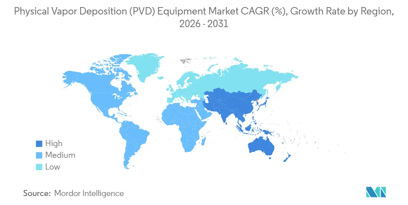
| Fastest Growing Market | Asia Pacific |
| Largest Market | Asia Pacific |
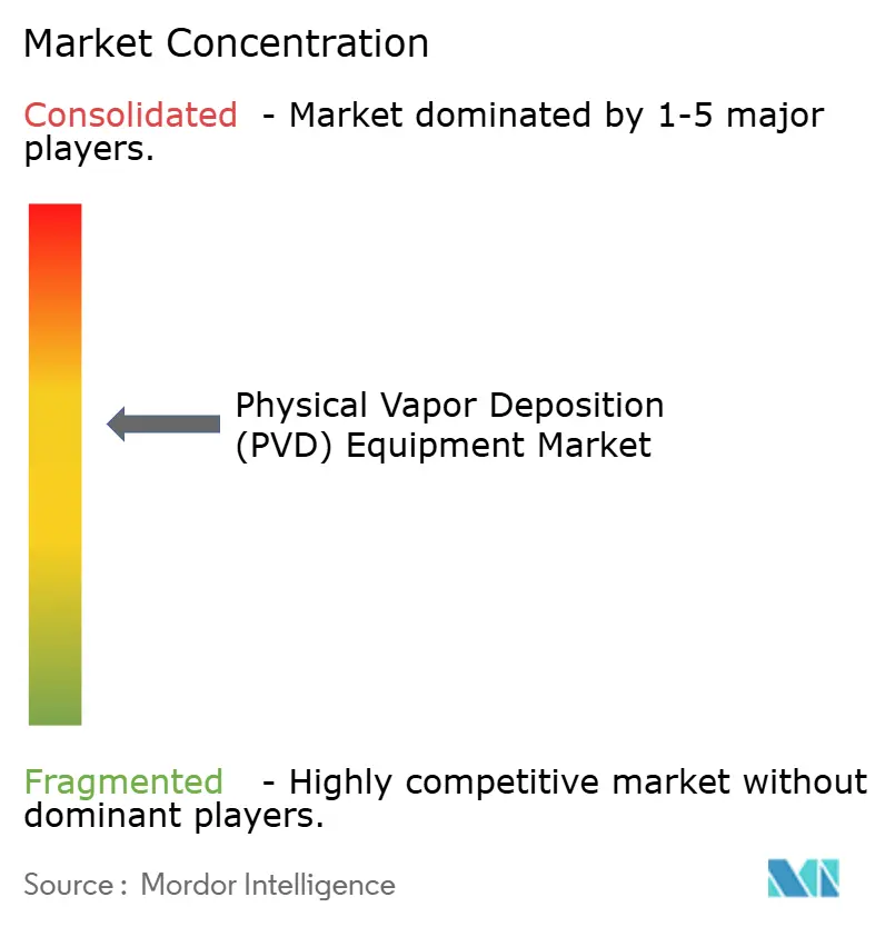
| Market Concentration | Medium |
Major Players
*Disclaimer: Major Players sorted in no particular order Image © Mordor Intelligence. Reuse requires attribution under CC BY 4.0. |
|
Physical Vapor Deposition (PVD) Equipment Market Analysis by Mordor Intelligence
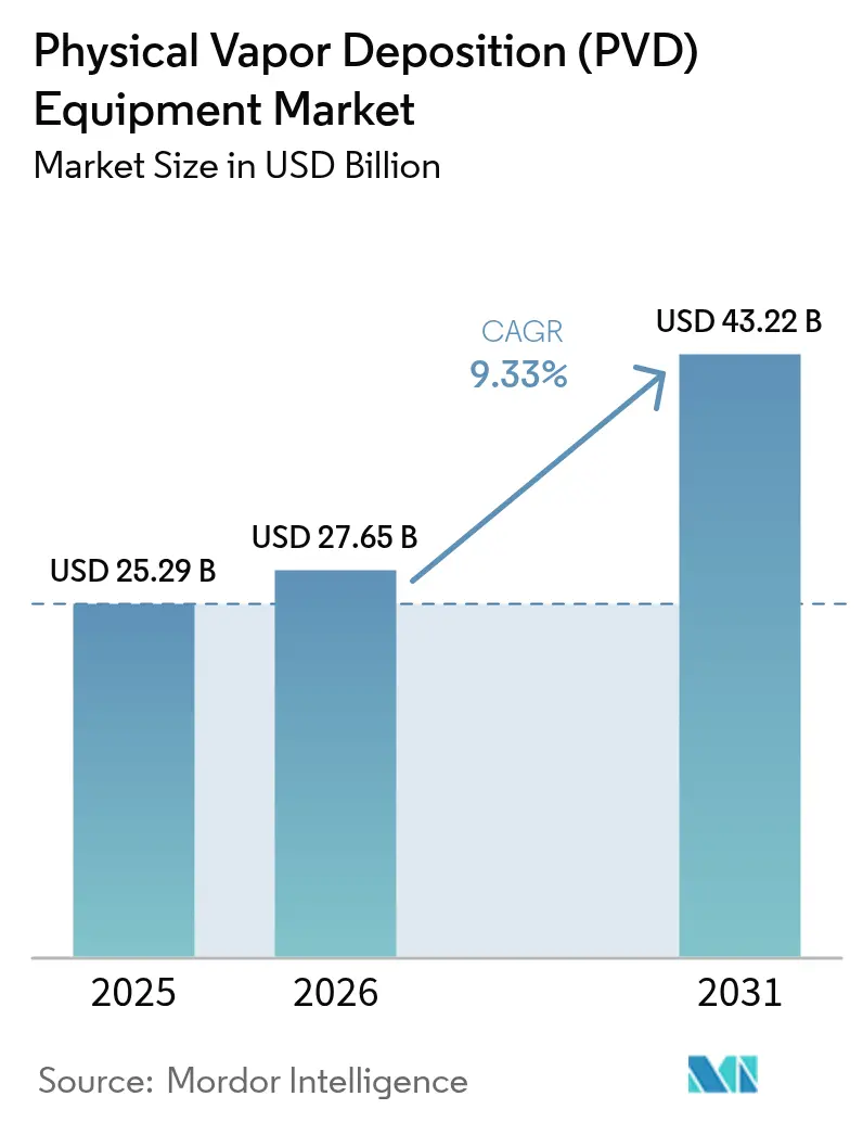
Physical Vapor Deposition Equipment Market size in 2026 is estimated at USD 27.65 billion, growing from 2025 value of USD 25.29 billion with 2031 projections showing USD 43.22 billion, growing at 9.33% CAGR over 2026-2031.
Strong demand for gate-all-around transistors below 3 nanometers, expanding use of biocompatible thin films in orthopaedic and cardiovascular implants, and durability mandates for electric-vehicle drivetrain parts form the backbone of near-term growth. Magnetron sputtering retains a production advantage for copper and tantalum interconnects, while ion plating is gaining ground in high-mix, decorative, and cutting-tool settings where dense, adherent films on complex shapes are critical. Semiconductor capital-expenditure waves in Taiwan, South Korea, the United States, and the European Union continue to funnel multi-chamber orders to tool vendors, and government incentives that localize equipment supply chains are shortening replacement cycles. At the same time, competition from atomic-layer deposition is sharpening performance benchmarks, pushing PVD suppliers toward cluster tools that integrate deposition, pre-clean, and anneal in a single vacuum transfer path.
Key Report Takeaways
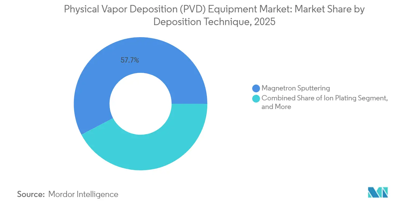
- By deposition technique, magnetron sputtering is expected to lead with a 57.68% revenue share in 2025, while ion plating is forecast to expand at a 10.72% CAGR to 2031.
- By end user, microelectronics captured 42.05% of 2025 turnover, whereas cutting tools are projected to log the fastest 11.28% CAGR through 2031.
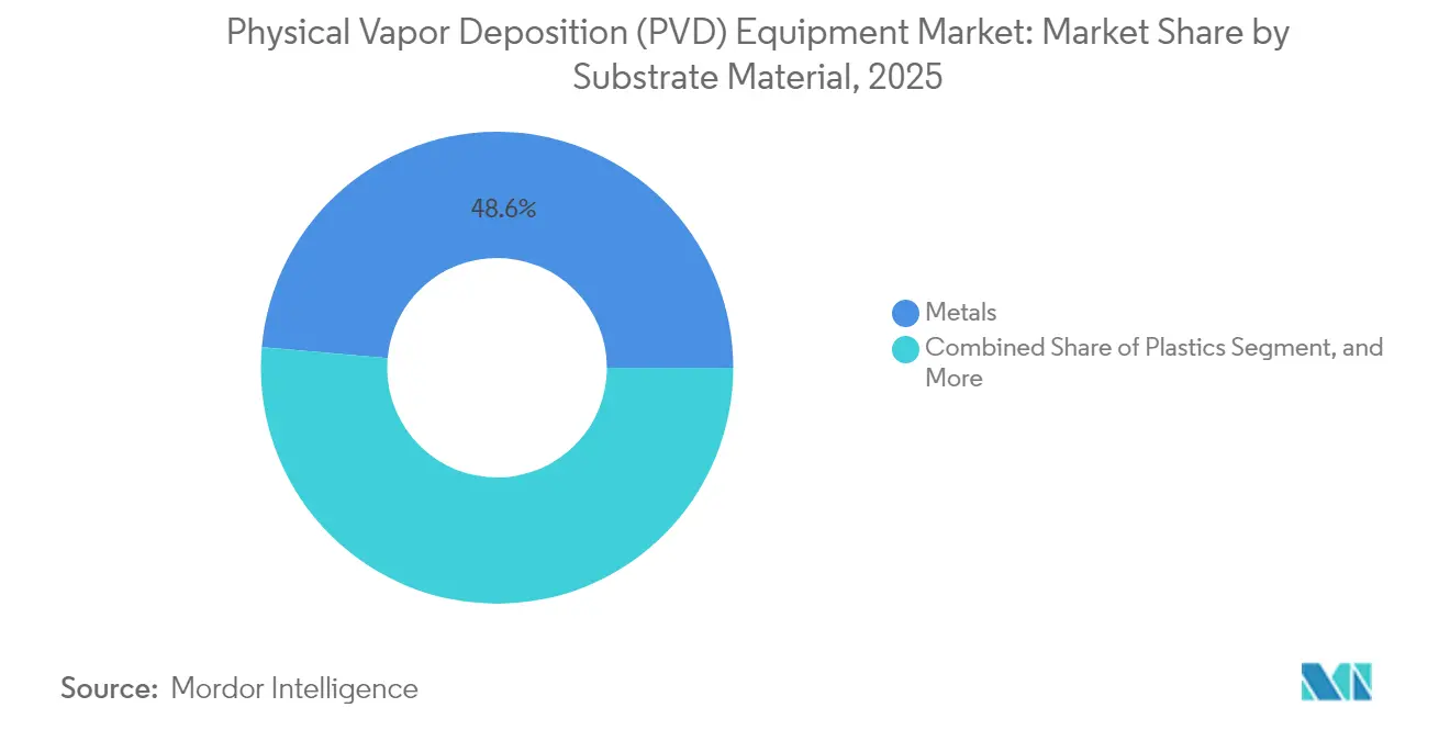
- By substrate material, metals held 48.61% of the physical vapor deposition (PVD) equipment market share in 2025, while plastics usage is expected to grow at 9.98% through 2031.
- By coating thickness, the 1–3-micron category accounted for 40.92% of the 2025 volume; however, sub-micron layers are poised to rise at a 10.12% CAGR through 2031.
- By geography, the Asia Pacific generated 37.88% of global revenue in 2025 and is projected to record a 9.97% CAGR through 2031.
Note: Market size and forecast figures in this report are generated using Mordor Intelligence’s proprietary estimation framework, updated with the latest available data and insights as of 2026.
Global Physical Vapor Deposition (PVD) Equipment Market Trends and Insights
Drivers Impact Analysis*
| Driver | (~) % Impact on CAGR Forecast | Geographic Relevance | Impact Timeline |
|---|---|---|---|
| Rising Demand for Advanced Microelectronics and Semiconductor Scaling | +2.80% | Global, with concentration in Asia Pacific (Taiwan, South Korea, China) and North America | Medium term (2-4 years) |
| Growth of High-Performance Medical Implants Requiring Biocompatible Coatings | +1.20% | North America and Europe, expanding to Asia Pacific | Long term (≥ 4 years) |
| Increasing Adoption of Thin-Film Solar Modules | +1.50% | Asia Pacific (China, India), North America, Europe | Medium term (2-4 years) |
| Government Incentives for Onshore Semiconductor Equipment Manufacturing | +1.90% | North America (CHIPS Act), Europe (EU Chips Act), Asia Pacific (Japan, South Korea subsidies) | Short term (≤ 2 years) |
| Demand for Wear-Resistant Coatings in Electric Vehicle Drivetrain Components | +1.40% | Global, with early traction in Europe and China | Medium term (2-4 years) |
| Integration of PVD in Flexible Electronics Manufacturing | +0.90% | Asia Pacific (South Korea, China), spill-over to North America | Long term (≥ 4 years) |
| Source: Mordor Intelligence | |||
Rising Demand for Advanced Microelectronics and Semiconductor Scaling
Node migration to 2-nanometer gate-all-around transistors requires ultra-thin tantalum-nitride work-function layers deposited by magnetron sputtering at high throughput, driving multi-chamber demand in Taiwan, South Korea, and the United States.[1]Applied Materials, “Endura Platform for Semiconductor Manufacturing,” APPLIEDMATERIALS.COM Every new 40,000 wafer-per-month fab needs 25-30 sputter chambers for copper barrier, seed, and capping steps. Cluster integration that combines pre-clean, deposition, and anneal inside one vacuum envelope cuts particulate defects by 30% and is now a de-facto specification in 3 nanometre ramps.[2]IEEE Staff, “Process Control at 2 nm,” IEEE.ORG Advanced packaging adds further pull, because hybrid-bonded chiplets and through-silicon vias require copper redistribution at 500 nanometers to 2 microns.
Memory producers are qualifying PVD tungsten for 300-layer 3D NAND, citing tighter step-coverage control than chemical vapor routes. Most importantly, local subsidies that favour domestic tool sourcing elevate regional suppliers and shorten purchasing cycles from four to three years in leading-edge fabs.
Government Incentives for Onshore Semiconductor Equipment Manufacturing
The United States CHIPS and Science Act released USD 39 billion in manufacturing grants and USD 11 billion in loans, stipulating that 30% of equipment spend must originate from U.S. vendors.[3]U.S. Department of Commerce, “CHIPS and Science Act Implementation,” COMMERCE.GOV Intel alone earmarked more than 200 PVD chambers for Arizona, Ohio, and New Mexico lines. Europe’s EUR 43 billion (USD 47.7 billion) Chips Act channels EUR 30 billion (USD 33.3 billion) into Intel Magdeburg and supports TSMC’s Dresden joint venture, again with local-content clauses that lift orders for Veeco, Oerlikon, and Von Ardenne.[4]European Commission, “EU Chips Act,” EC.EUROPA.EU Japan, South Korea, and China run parallel subsidy programs that either cover 40% of capex or offer multi-year tax holidays on imported equipment, effectively lowering payback periods below five years.
As new fabs come online, the PVD equipment market enjoys synchronized demand in three continents, stabilizing order books against cyclical semiconductor downturns.
Increasing Adoption of Thin-Film Solar Modules
Cadmium-telluride and heterojunction solar lines deploy large-area magnetron sputtering for transparent conductive oxides, lifting PVD revenue per gigawatt to USD 15-20 million. Heterojunction shipments climbed from 8% in 2023 to 12% in 2024, each gigawatt requiring six to eight inline sputter coaters.
First Solar added 3.3 gigawatts of capacity in Ohio in 2024, while India’s USD 2.4 billion production-linked incentive scheme ties import duties to domestic equipment adoption. Perovskite-silicon tandem prototypes already specify nickel-oxide and indium-zinc-oxide PVD layers, and although mass production awaits IEC durability standards, early tool pilots suggest a 30% uptick in chamber count per square meter of output. These trends collectively boost non-semiconductor share of the PVD equipment market, smoothing revenue volatility tied to logic and memory nodes.
Demand for Wear-Resistant Coatings in Electric Vehicle Drivetrain Components
Torque-rich single-speed transmissions spin at 20,000 rpm and expose gears and bearings to higher Hertzian loads than combustion engines. Titanium-aluminium-nitride and chromium-nitride ion-plated layers cut friction and heat, enabling automakers to offer 300,000-kilometer powertrain warranties. Oerlikon’s coating centers reported 35% year-over-year revenue growth in 2024, supported by Volkswagen and Stellantis sourcing drivetrain parts in Europe and China. Diamond-like carbon layers, deposited via cathodic arc or filtered sputter, reduce dry-running coefficients of friction below 0.10 and support oil-less auxiliary pump architectures that raise battery-to-wheel efficiency by 2-3%.
Although no regulation prescribes surface treatments, warranty differentiation pushes tier-one suppliers to standardize on PVD, expanding aftermarket and refurbishment opportunities for regional coaters.
Restraints Impact Analysis*
| Restraint | (~) % Impact on CAGR Forecast | Geographic Relevance | Impact Timeline |
|---|---|---|---|
| High Capital Investment | -1.60% | Global, acute in emerging markets and small-to-medium enterprises | Short term (≤ 2 years) |
| Competition from Alternative Deposition Technologies such as ALD and CVD | -1.10% | Global, concentrated in advanced semiconductor nodes | Medium term (2-4 years) |
| Supply Chain Vulnerabilities for High-Purity Target Materials | -0.70% | Global, with acute impact in North America and Europe | Medium term (2-4 years) |
| Stringent Environmental Regulations on Plasma Emissions | -0.50% | Europe and North America, expanding to Asia Pacific | Long term (≥ 4 years) |
| Source: Mordor Intelligence | |||
High Capital Investment
A state-of-the-art magnetron sputtering cluster for 300-millimeter wafers costs USD 3-5 million, while fully configured logic lines often install 20-30 chambers, pushing upfront outlays above USD 100 million before qualification. Service contracts, spare kits, and consumable targets add a further 15-20% to lifetime ownership. Smaller coaters in cutting-tool or decorative markets face USD 0.5-0.8 million ticket prices per cathodic-arc tool and must process 10,000-15,000 cycles to break even.
Although leasing and pay-per-wafer models lower entry barriers by 40%, they transfer utilization risk to financiers and raise per-part cost by roughly 10%. Consequently, new entrants gravitate toward modular single-chamber designs, limiting large-cluster penetration outside tier-one fabs.
Competition from Alternative Deposition Technologies Such as ALD and CVD
Atomic-layer deposition captured about 25% of thin-film equipment revenue in leading-edge fabs during 2024 because its self-limiting chemistries deliver uniformity inside 50:1 aspect-ratio features that sputter guns cannot reach. Hafnium-oxide high-k dielectrics under 2 nanometers now ship predominantly on ALD platforms supplied by Lam Research and Tokyo Electron. Chemical-vapor deposition maintains throughput advantages in bulk tungsten and silicon nitride.
Hybrid flows are emerging: TSMC’s N2 process employs ALD for gate dielectrics, PVD for seed layers, and electroplating for fill, meaning PVD retains metallization but loses oxide layers. Tight competition is forcing PVD vendors to integrate ALD modules within the same transfer platform or risk socket erosion in sub-3-nanometer nodes.
*Our forecasts treat driver/restraint impacts as directional, not additive. The impact forecasts reflect baseline growth, mix effects, and variable interactions.
Segment Analysis
By Deposition Technique: Magnetron Sputtering Anchors Interconnect Metallization
Magnetron sputtering delivered 57.68% of 2025 revenue because its low-energy ion bombardment spreads copper and tantalum films with <2% across-wafer non-uniformity, the tightest window tolerated in 300-millimeter back-end-of-line runs. The physical vapor deposition (PVD) equipment market size for magnetron tools is projected to rise at 8.42% CAGR, reinforced by logic and 3D NAND ramps that each consume 6-8 chambers per metallization loop. Ion plating, although currently below 15% share, is forecast to progress at 10.72% through 2031 as cutting-tool and decorative-hardware producers invest in dense columnar films that outperform electroplated chrome on adhesion and corrosion. Cost-of-ownership gains favour rotary cathodes and closed-loop plasma monitors that extend target life by 50% and slash scrap below 3%. Cathodic-arc and electron-beam PVD stay niche, serving extreme-hardness or low-temperature optics where particle contamination or polymer shrinkage is mission-critical. With SEMI standards agnostic to technique selection, buyers weigh throughput, consumables, and uptime, reinforcing magnetron dominance yet leaving whitespace for specialized approaches that address emerging flexible-electronics demands.
Ion-plating vendors now market hybrid chambers that flip between high-power impulse sputtering and DC glow to accommodate titanium-aluminium-nitride, zirconium-nitride, and diamond-like carbon in consecutive cycles. Such flexibility halves cleaning downtime and boosts revenue per floor area in coating centers. Meanwhile, Applied Materials’ fourteen-station Endura cluster locks customers into proprietary pre-clean, barrier, seed, and cap recipes, an ecosystem that secures pull-through consumables and inflates switching costs. Consequently, the physical vapor deposition (PVD) equipment market continues to reward integrated platform depth on one end and nimble single-chamber agility on the other.


By End User: Microelectronics Dominates While Cutting Tools Surge
Microelectronics secured 42.05% of 2025 turnover because foundries rely on PVD for copper dual-damascene, tantalum-nitride barriers, and aluminium bond pads. The PVD equipment market size for microelectronics could pass USD 26.6 billion by 2031, assuming node migrations and hybrid-bonded chiplets maintain current capex vectors. Cutting tools, however, are pacing fastest at 11.28% CAGR as aerospace and automotive machining shifts toward dry, high-speed protocols where titanium-aluminium-nitride triples insert life. Ion-plating site rollouts in Mexico, India, and Eastern Europe highlight geographic realignment of metal-cutting supply chains. Medical devices hold roughly 14% share, with FDA 510(k) filings showing over forty PVD-coated orthopaedics implants cleared in 2024 alone. Solar products contribute 11% of revenue, yet capacity expansions in Ohio, Malaysia, and Gujarat position thin-film PV to outgrow global module averages through 2028.
Regulatory processes shape adoption timelines differently across end users. Medical implants require 18-24 months of biocompatibility testing per new coating, while semiconductor purchase decisions compress into 6-9-month windows around node releases. Cutting-tool services face minimal accreditation and can commercialize recipes within weeks. As a result, revenue diversity stabilizes aggregate growth for the PVD equipment market, cushioning cyclical swings tied to silicon fabs.
By Substrate Material: Metals Lead as Plastics Gain Presence in Flexible Displays
Metals attracted 48.61% of 2025 billings since stainless-steel tooling, titanium implants, and aluminium trim are default workpieces for wear-resistant and decorative films. Plastics, led by polyethylene terephthalate and polyimide, are projected to expand at 9.98% CAGR because roll-to-roll coating lines now deposit aluminium-oxide and silicon-nitride moisture barriers for foldable-OLED encapsulation at temperatures below 80 °C. The PVD equipment market share for glass stands near 18%, propelled by low-emissivity architectural panes that reduce space-heating loads. Ceramic substrates, although below 10% share, anchor high-value dental crowns and zirconia cutting inserts, where PVD layers extend service life and lower revision rates.
Large-area sputter coaters exceed 3 meters in web width for architectural glass, driving unit values above USD 25 million and reinforcing European vendor strength. Conversely, plastics coating systems prioritize low thermal budget and line speed, pushing toolmakers to refine pulsed-DC power supplies that sustain dense plasma without substrate warpage. As foldable displays progress from smartphones to tablets and automotive interiors, plastics uptake is poised to narrow the metals gap inside the PVD equipment market.
By Coating Thickness: Sub-Micron Films Accelerate in Advanced Nodes
Coatings between 1 and 3 microns retained 40.92% of 2025 volume because cutting-tool wear layers peak in this range. Yet sub-micron stacks are projected to clock a 10.12% CAGR, reflecting work-function metals and copper seeds under 50 nanometers in gate-all-around and hybrid-bond packaging lines. The PVD equipment market size for sub-micron applications grows in lockstep with 2 nanometer ramps that demand <1.5 nanometer tantalum-nitride blankets. Electron-beam optical coatings and flexible-display barriers also fall below 100 nanometers, boosting demand for high-precision quartz-crystal monitoring and in-situ spectroscopic control. Thicker 3–5-micron decorative films hold steady in watches and automotive trim, while >5-micron thermal barriers stay niche at roughly 11% share.
Tool vendors now advertise process windows delivering 1.8% thickness uniformity on 1-nanometer films, a capability that vaults cluster adoption and justifies premium pricing. Meanwhile, cutting-tool service centers fine-tune recipe stacks in 0.2 micron increments to balance edge sharpness and crater resistance, illustrating the tight interplay between film thickness and application performance.
Geography Analysis
Asia Pacific commanded 37.88% of 2025 sales and is positioned to log a 9.97% CAGR through 2031, underpinned by Taiwan Semiconductor Manufacturing Company’s USD 165 billion multiyear spend, Samsung Foundry’s Pyeongtaek and Hwaseong expansions, and the People’s Republic of China’s goal of 70% equipment self-reliance by decade-end. Japan’s METI subsidies reimburse up to 40% of qualifying capex, encouraging ULVAC and Tokyo Electron to localize sputter chamber components and shorten lead times. India’s USD 10 billion chip incentive accepted three 300-millimeter fab proposals, each projecting 25-30 PVD chambers and potentially adding USD 500 million in tool orders by 2028.
North America held 27.74% share in 2025. The CHIPS Act funded Intel, TSMC, Samsung, and Micron, each stipulating domestic supply requirements that favour U.S. chamber and target plants. Intel’s Ohio campus alone plans over 200 PVD tools for 18A and 14A production, representing a USD 1 billion opportunity. Micron’s high-bandwidth-memory site in New York will consume tungsten and copper sputter modules for vertical DRAM stacks, while Canada’s compound-semiconductor cluster invests in electron-beam PVD for gallium-nitride RF devices.
Europe finished 2025 at 21.86% share. The European Union converted EUR 43 billion (USD 47.7 billion) of incentives into Intel Magdeburg, TSMC Dresden, and STMicroelectronics silicon-carbide expansions. German onshore-content rules define a 30% local-value floor, creating tailwinds for Oerlikon, Veeco, and Von Ardenne. France’s EUR 500 million (USD 555 million) advanced-packaging program adds pilot sputter loops for copper redistribution and hybrid bonding. Strict plasma-emission mandates in the region favour tools with built-in fluorinated-gas abatement, cementing competitive advantage for suppliers that bundle environmental compliance.

Competitive Landscape
The physical vapor deposition (PVD) equipment market shows moderate concentration. The top five companies Applied Materials, ULVAC, Veeco Instruments, Tokyo Electron, and Lam Research captured roughly 55% of 2024 shipments through cluster portfolios that fuse sputter, etch, and metrology modules. Applied Materials shipped over 300 Endura chambers in 2024, commanding back-end metallization, while ULVAC’s rotary-cathode systems trimmed target usage by 40% and led Japan’s display lines. Veeco differentiated on ion-beam etch-plus-deposit hybrids that raise advanced-packaging throughput by 25%.
Below the top tier, specialists such as Angstrom Engineering, AJA International, and Denton Vacuum supply sub-USD 500,000 single-chamber tools to universities and pilot fabs in under six-month lead times. Service-oriented players Oerlikon Balzers and Platit manage more than 150 coating centers worldwide, leveraging ion-plating recipes that extend carbide tool life threefold. Chinese entrants like Shincron price 20% lower in automotive coatings, stoking price pressure in mature segments. Strategic differentiation hinges on process integration, smart sensors, and consumables lock-in: Applied Materials’ Sym3 Y embeds real-time thickness control that pulls scrap rates below 2%, justifying a 15% premium.
Hybrid PVD-ALD clusters are emerging as the next battleground at 3 nanometers and below, prompting cross-licensing deals between sputter and ALD specialists. Overall, technology breadth, service footprint, and ownership economics outweigh pure hardware specs.
Physical Vapor Deposition (PVD) Equipment Industry Leaders
-
Advanced Energy Industries Inc.
-
Angstrom Engineering Inc.
-
Veeco Instruments Inc.
-
Applied Materials Inc.
-
Platit AG
- *Disclaimer: Major Players sorted in no particular order

Recent Industry Developments
- January 2025: Oerlikon Balzers installed two additional ion-plating lines in Suzhou, China, aiming for 2 million tool-coating cycles per year.
- October 2024: Applied Materials shipped its 500th Endura Copper Barrier Seed system to a leading Asian logic customer.
- September 2024: ULVAC won a USD 45 million order for 12 rotary-cathode sputter chambers at TSMC’s second Kumamoto fab.
- August 2024: Intel secured USD 8.5 billion in CHIPS Act grants and loans to expand sites in Arizona, Ohio, and New Mexico, each committing to >200 PVD chambers.


Global Physical Vapor Deposition (PVD) Equipment Market Report Scope
The Physical Vapor Deposition (PVD) Equipment Market Report is Segmented by Deposition Technique (Cathodic Arc Deposition, Electron Beam PVD, Magnetron Sputtering, Ion Plating, Other Deposition Techniques), End User (Microelectronics, Medical Devices and Equipment, Solar Products, Cutting Tools, Other End Users), Substrate Material (Metals, Plastics, Glass, Ceramics, Others), Coating Thickness (Below 1 Micron, 1-3 Micron, 3-5 Micron, Above 5 Micron), and Geography (North America, Europe, Asia Pacific, Middle East, Africa, South America). The Market Forecasts are Provided in Terms of Value (USD).
| Cathodic Arc Deposition |
| Electron Beam PVD |
| Magnetron Sputtering |
| Ion Plating |
| Other Deposition Techniques |
| Microelectronics |
| Medical Devices and Equipment |
| Solar Products |
| Cutting Tools |
| Other End Users |
| Metals |
| Plastics |
| Glass |
| Ceramics |
| Others Substrate Material |
| Below 1 Micron |
| 1 - 3 Micron |
| 3 - 5 Micron |
| Above 5 Micron |
| North America | United States |
| Canada | |
| Mexico | |
| Europe | Germany |
| France | |
| United Kingdom | |
| Italy | |
| Spain | |
| Rest of Europe | |
| Asia Pacific | China |
| Japan | |
| South Korea | |
| India | |
| Rest of Asia Pacific | |
| Middle East | Saudi Arabia |
| United Arab Emirates | |
| Turkey | |
| Rest of Middle East | |
| Africa | South Africa |
| Nigeria | |
| Rest of Africa | |
| South America | Brazil |
| Argentina | |
| Rest of South America |
| By Deposition Technique | Cathodic Arc Deposition | |
| Electron Beam PVD | ||
| Magnetron Sputtering | ||
| Ion Plating | ||
| Other Deposition Techniques | ||
| By End User | Microelectronics | |
| Medical Devices and Equipment | ||
| Solar Products | ||
| Cutting Tools | ||
| Other End Users | ||
| By Substrate Material | Metals | |
| Plastics | ||
| Glass | ||
| Ceramics | ||
| Others Substrate Material | ||
| By Coating Thickness | Below 1 Micron | |
| 1 - 3 Micron | ||
| 3 - 5 Micron | ||
| Above 5 Micron | ||
| By Geography | North America | United States |
| Canada | ||
| Mexico | ||
| Europe | Germany | |
| France | ||
| United Kingdom | ||
| Italy | ||
| Spain | ||
| Rest of Europe | ||
| Asia Pacific | China | |
| Japan | ||
| South Korea | ||
| India | ||
| Rest of Asia Pacific | ||
| Middle East | Saudi Arabia | |
| United Arab Emirates | ||
| Turkey | ||
| Rest of Middle East | ||
| Africa | South Africa | |
| Nigeria | ||
| Rest of Africa | ||
| South America | Brazil | |
| Argentina | ||
| Rest of South America | ||


Key Questions Answered in the Report
What is the projected value of the physical vapor deposition PVD equipment market by 2031?
The physical vapor deposition (PVD) equipment market is forecast to reach USD 43.22 billion by 2031.
Which deposition technique currently dominates revenue?
Magnetron sputtering led with 57.68% revenue share in 2025.
Why is Asia Pacific growing fastest in PVD equipment demand?
Massive capital spending by TSMC, Samsung, and Chinese foundries, supported by regional subsidies, drives a 9.97% CAGR through 2031.
How do capital costs impact smaller PVD service providers?
Cluster tools can exceed USD 5 million, forcing smaller firms toward single-chamber systems or leasing models that shift utilization risk.
What role does PVD play in electric-vehicle drivetrains?
Ion-plated titanium-aluminum-nitride and chromium-nitride coatings extend gear and bearing life, enabling 300,000 kilometer warranties.
Is atomic-layer deposition replacing PVD in semiconductors?
ALD is gaining ground for ultrathin dielectrics, but PVD retains advantages in metallization due to lower copper resistivity and higher throughput.
Page last updated on:


