Semiconductor Packaging Market Size and Share
Market Overview
| Study Period | 2019 - 2030 |
| Market Size (2025) | USD 49.88 Billion |
| Market Size (2030) | USD 81.22 Billion |
| Growth Rate (2025 - 2030) | 10.24% CAGR |
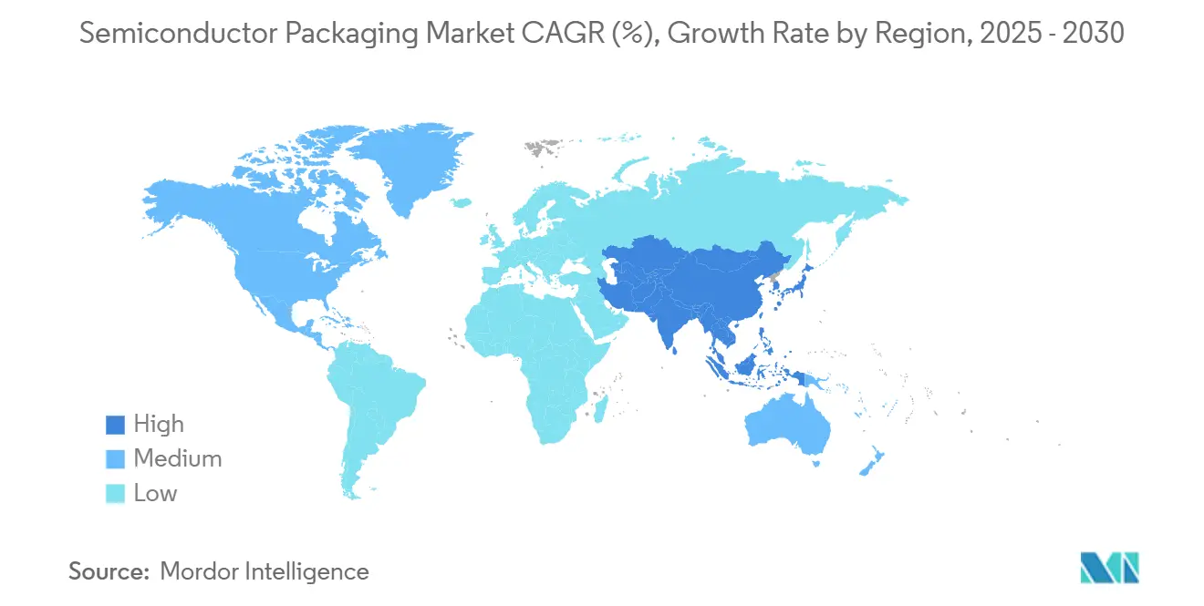
| Fastest Growing Market | North America |
| Largest Market | Asia |
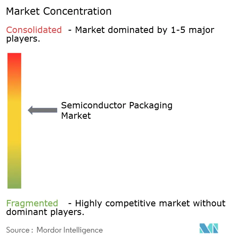
| Market Concentration | Medium |
Major Players
*Disclaimer: Major Players sorted in no particular order Image © Mordor Intelligence. Reuse requires attribution under CC BY 4.0. |
|
Semiconductor Packaging Market Analysis by Mordor Intelligence
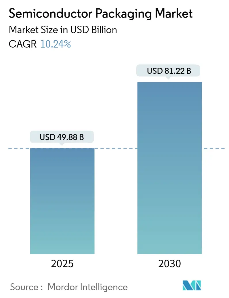
The semiconductor packaging market size stood at USD 49.88 billion in 2025 and is projected to reach USD 81.22 billion by 2030, advancing at a 10.24% CAGR over 2025-2030. [1]Cheng Ting-Fang, “TSMC moves closer to next-gen packaging for Nvidia, Google AI chips,” Nikkei Asia, asia.nikkei.comA shift from cost-driven assembly toward performance-critical integration underpins this growth. Demand for 2.5D and 3D architectures has risen sharply as AI workloads call for high-bandwidth memory and superior thermal paths. Volume remains anchored in traditional wire-bond and lead-frame formats, yet value creation is migrating to fan-out wafer-level packaging (WLP) and chiplet-enabled interposers. Automotive electrification supports double-digit expansion in power-dense modules, while smartphone and PC refresh cycles sustain baseline volumes in the consumer segment. Regionally, Asia commands more than half of global output, but North America registers the highest CAGR thanks to CHIPS Act incentives that fund new back-end fabs.[2]U.S. Department of Commerce, “CHIPS for America Announces up to $300 million in Funding to Boost U.S. Semiconductor Packaging,” commerce.gov Supply bottlenecks in ABF substrates and export restrictions on advanced tools are catalyzing geographic diversification and material innovation.
Key Report Takeaways
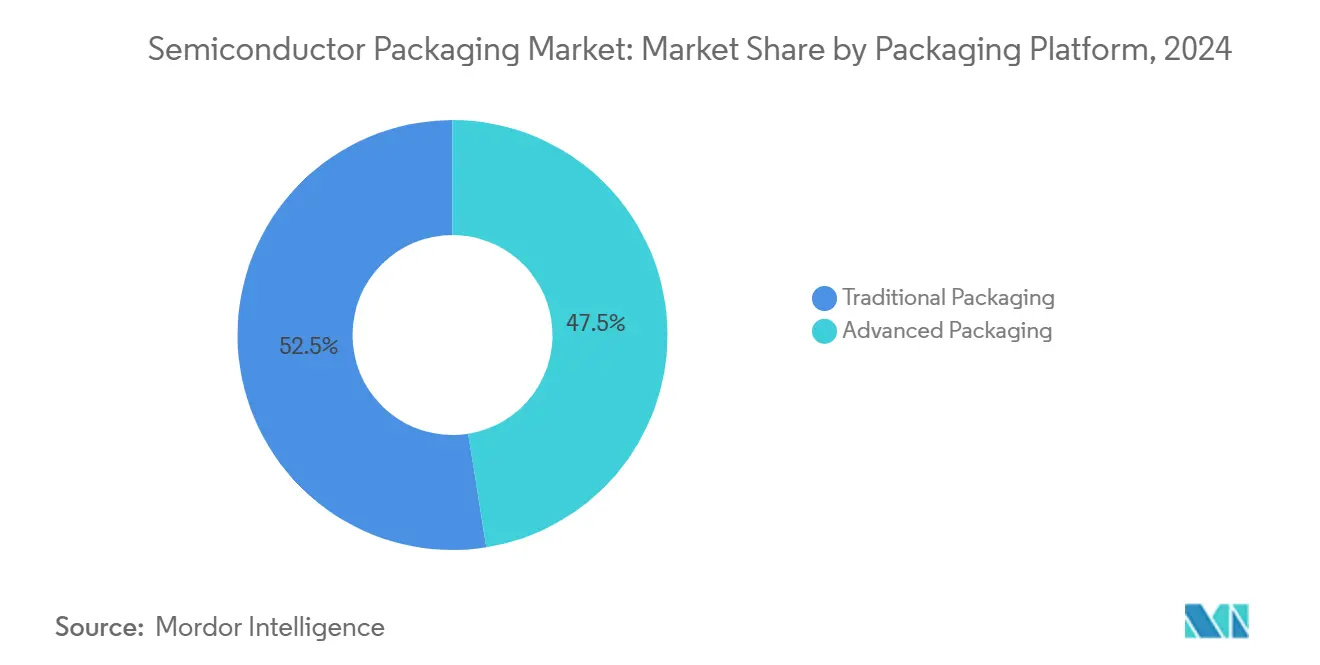
- By packaging platform, traditional formats held 52.5% of semiconductor packaging market share in 2024, whereas fan-out WLP is forecast to expand at 12.3% CAGR to 2030.
- By end-user industry, consumer electronics led with 43.8% revenue share of the semiconductor packaging market size in 2024; automotive is pacing the fastest growth at 10.3% CAGR through 2030.
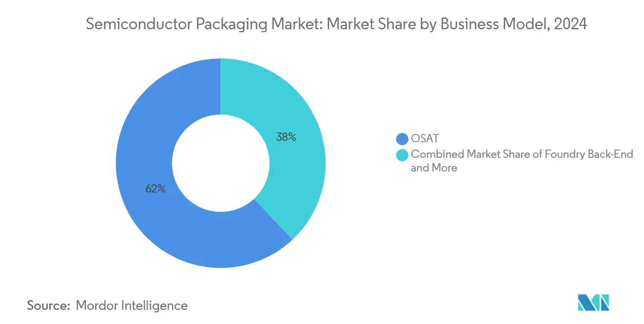
- By business model, the OSAT segment controlled 62.0% of global semiconductor packaging market share in 2024 while foundry back-end services are rising at 10.9% CAGR.
- By geography, Asia held 53.0% of the semiconductor packaging market in 2024; North America is poised for an 11.1% CAGR to 2030.
- ASE, Amkor and JCET jointly accounted for more than 30% share of advanced-technology revenue in 2024, reflecting scale advantages in hybrid bonding and SiP production
Global Semiconductor Packaging Market Trends and Insights
Drivers Impact Analysis
| Driver | (~) % Impact on CAGR Forecast | Geographic Relevance | Impact Timeline |
|---|---|---|---|
| AI accelerator boom driving 2.5D/3D interposers | +2.8% | Global (Taiwan, US, China) | Medium term (2-4 years) |
| Electrified-vehicle power packages | +1.9% | North America & APAC | Long term (≥4 years) |
| US-EU CHIPS incentives creating local back-end fabs | +1.4% | North America & EU | Long term (≥4 years) |
| 5G RF-SiP demand in China & Korea | +1.2% | APAC core | Short term (≤2 years) |
| Panel-level packaging for low-cost IoT | +0.9% | Global (APAC hubs) | Medium term (2-4 years) |
| Chiplet architectures powering high-density interposers | +1.6% | Global (US design, Taiwan mfg.) | Medium term (2-4 years) |
Source: Mordor Intelligence
AI accelerator boom driving 2.5D/3D interposers
TSMC’s CoWoS capacity is doubling from 120,000 to 240,000 units between 2023 and 2024, yet it still cannot fully meet hyperscaler demand. The capacity gap is stimulating alternative panel-level flows and 3.5D stacking trials that aggregate more than 6,000 mm² of silicon per package. [3]James Morra, “Broadcom Bets on 3.5D Packaging Technology to Build Bigger AI Chips,” Electronic Design, electronicdesign.com Advanced packaging has therefore moved from a cost center to a strategic lever for AI system performance
Electrified-vehicle power packages in United States & Asia
onsemi’s EliteSiC platform awarded by Volkswagen exemplifies the migration toward integrated power modules with superior heat dissipation. ROHM’s 6-in-1 molded SiC modules deliver triple the power density of prior. These innovations concentrate in US and Asian supply chains that can meet stringent automotive qualification.
US-EU CHIPS incentives creating local back-end fabs
The CHIPS Act earmarks USD 300 million exclusively for advanced packaging R&D, subsidizing test lines in Georgia, California and Arizona. Intel’s USD 3.5 billion Foveros site in New Mexico anchors domestic 3D integration capacity. Comparable funds in the EU aim to de-risk automotive and defense electronics from Asian supply disruptions.
5G RF-SiP demand in China & Korea
JCET’s heterogeneous RF-SiP for power amplifiers lifts integration density 1.5× over prior nodes j. While premium handsets sustain innovation, mass-tier Android demand softness has tempered unit growth, pressing suppliers to optimize cost structures
Restraints Impact Analysis
| Restraint | (~) % Impact on CAGR Forecast | Geographic Relevance | Impact Timeline |
|---|---|---|---|
| ABF substrate supply crunch | -1.8% | Global (APAC acute) | Short term (≤2 years) |
| Yield challenges in 3D TSV/hybrid bonding | -1.3% | Global (Taiwan, Korea, US) | Medium term (2-4 years) |
| Export controls on advanced packaging tools to China | -0.9% | China primary | Long term (≥4 years) |
| Thermal dissipation limits in fan-out WLP @ <5 nm | -0.7% | Global advanced nodes | Medium term (2-4 years) |
Source: Mordor Intelligence
ABF substrate supply crunch
Nittobo’s 20% price hike in August 2025 exposes systemic material tightness that particularly affects flip-chip BGA lines. Limited qualified capacity in Taiwan and Japan prolongs lead times and pushes OEMs to explore glass-core or silicon-core alternatives.
Yield challenges in 3D TSV/hybrid bonding
Copper-to-copper hybrid bonding tolerances under 0.5 nm and TSV aspect ratios beyond 10:1 multiply defect risks across stacked. NVIDIA’s Blackwell program reportedly hit yield escapes tied to CoWoS-L thermomechanical stress.
Segment Analysis
By Packaging Platform: Advanced technologies drive value migration
Traditional wire-bond and lead-frame offerings still dominated shipments with 52.5% semiconductor packaging market share in 2024, ensuring that consumer electronics and industrial devices retain affordable bill-of-materials costs. However, Fan-out WLP outpaces every other format at a 12.3% CAGR, signaling the semiconductor packaging market’s move toward substrate-free redistribution layers that shrink z-height and boost I/O density. Flip-chip bridges the gap by pairing fine-pitch bumps with moderate cost, while SiP and PoP architectures enable vertical stacking for space-constrained handsets.
On the advanced front, 2.5D interposers position high-bandwidth memory adjacent to AI logic, and 3D stacks unlock latency gains. Embedded-die and panel-level flows attract new entrants focused on IoT price points, demonstrating that the semiconductor packaging market is splitting into premium performance nodes and ultra-low-cost volume plays. In contrast, panel-level lines deliver sub-USD 0.10 per pin, a ratio that underscores divergent cost structures. As a result, equipment makers have segmented their portfolios: high-accuracy bonder clusters for 3 µm alignment coexist with large-panel MOLD lines aimed at IoT tags. Such bifurcation redefines supplier positioning inside the semiconductor packaging market.
Note: Segment shares of all individual segments available upon report purchase
By Packaging Material: Organic substrates dominate amid innovation pressure
Organic ABF substrates carried 41.5% revenue in 2024, underpinning the mainstream flip-chip ecosystem. Yet semiconductor packaging market size for bonding wires is set to grow 11.4% annually as automotive and industrial sectors extend the life of proven aluminum and gold wire packages. Leadframes persist in power applications that value copper heat-spreader performance. Encapsulation resins have progressed to high-thermal-conductivity grades, supporting next-generation SiC and GaN modules.
Glass substrates could displace organic builds after 2027. Intel and Samsung prototypes show 40% via pitch reduction and near-zero CTE mismatch, lowering warpage in 3D stacks. Thermal interface materials now integrate nano-diamond fillers, cutting junction-to-case resistance by 30% in 1,200 V traction inverters. Gold price spikes compressed margins for display driver IC packaging in 2025, motivating migration to copper column bumps
By Wafer Size: 300 mm drives efficiency while panel format emerges
The 300 mm wafer format captured 74.0% of the semiconductor packaging market share in 2024, confirming its status as the preferred choice for advanced back-end flows that balance processing efficiency with front-end tool compatibility. Smaller wafers of 200 mm or less remain viable for legacy analog, sensor, and power lines where conversion costs outweigh productivity gains. Larger formats enable economies of scale that are increasingly critical as device counts climb in smartphones, PCs, and industrial IoT nodes.
Panel-level processing on substrates of 450 mm or more represents the fastest-growing segment at a 12.5% CAGR through 2030 and is poised to increase the semiconductor packaging market size by lowering per-unit material consumption and cycle times. Warpage control, inline yield metrology and equipment standardization remain the chief hurdles, requiring joint development efforts between tool makers and high-volume packaging houses.
By Business Model: OSAT leadership faces foundry challenge
OSATs retained 62.0% of semiconductor packaging market share in 2024 owing to broad customer rosters and global footprints. Yet foundry back-end expansion at 10.9% CAGR signals vertical integration. TSMC’s Wafer Manufacturing 2.0 melds litho, test and CoWoS under one quote, blurring OSAT boundaries.
In response, ASE targets USD 1.6 billion advanced-packaging revenue in 2025 via strategic capex and co-design with system OEMs reuters.com. Start-ups such as Chipletz focus on serviceable accessible markets where bespoke interposer design aligns with AI inference cards, illustrating niche penetration strategies.
Note: Segment shares of all individual segments available upon report purchase
By End-User Industry: Consumer electronics leads while automotive accelerates
Smartphones, tablets and PCs ensured a 43.8% share of the semiconductor packaging market in 2024 as OEMs refreshed form factors and introduced generative-AI on-device capabilities. Nevertheless, the automotive vertical posts the highest CAGR at 10.3% on the back of EV inverter and ADAS domain-controller content growth.
Automotive-grade power modules command ASPs five times higher than mobile SoCs, expanding semiconductor packaging market size disproportionately versus unit volumes. Communications infrastructure contributes RF-SiP demand, while data-center HPC steers the most advanced architectures, closing the loop between AI algorithm roadmaps and physical integration choices.
Geography Analysis
Asia captured 53.0% of the semiconductor packaging market in 2024, cemented by Taiwan’s CoWoS monopoly and China’s scale in wire-bond assembly. JCET’s RMB 4.4 billion automotive plant in Jiangsu advances local competency in SiC power packages. South Korea benefits from memory-centric SiP, whereas Japan controls pivotal substrate chemistries, reinforcing a tightly knit regional cluster.
North America’s semiconductor packaging market is projected to post an 11.1% CAGR through 2030. CHIPS Act incentives amass USD 300 million for R&D lines, spawning hubs in Arizona, New Mexico and California. Partnerships such as TSMC-Amkor in Arizona build complete back-end ecosystems proximate to leading-edge wafer fabs. Canada cultivates photonics packaging, and Mexico offers low-cost final test for consumer ASICs.
Europe positions around automotive and industrial strength. German Tier-1s co-develop double-sided cooled SiC modules targeting 9 kW/L inverter density, catalyzing niche OSAT investment. The Netherlands pushes high-frequency optical transceiver packaging that aligns with vertical-cavity surface-emitting laser (VCSEL) adoption. Middle East and Africa remain emerging, primarily outsourcing assembly to Asian hubs yet planning domestic lines for secure IoT and defense electronics under sovereign mandates.
Competitive Landscape
Competitive intensity pivots from price to technology. TSMC leverages foundry know-how to dominate 2.5D interposers while Samsung employs H-cube to blend memory and logic for mobile AI. ASE and Amkor spread risk across 40+ facilities, focusing on yield learning and design-for-manufacturability services. JCET scales SiP lines running automotive AEC-Q100 flows. Intel’s Foveros plant embodies a strategic leap to regain packaging leadership, offering 50 µm die-to-die pitch for client and data-center platforms.
Barriers to entry include capex intensity, substrate supply security, and customer co-development lock-ins. Consequently, consolidation through M&A—e.g., Empyrean’s purchase of Xpeedic—reflects a bid to aggregate EDA and packaging IP under one roof
Semiconductor Packaging Industry Leaders
-
ASE Technology Holding Co., Ltd.
-
Amkor Technology, Inc.
-
JCET Group Co., Ltd.
-
Siliconware Precision Industries Co., Ltd.
-
Powertech Technology Inc.
- *Disclaimer: Major Players sorted in no particular order
Recent Industry Developments
- June 2025: ASE and AMD partner to raise data-center efficiency by 50% while trimming power 6.5%, evaluating Instinct MI300 GPUs for AI workloads
- June 2025: Infineon unveils trench-based SiC super-junction MOSFETs, targeting traction inverters with first 1,200 V devices in ID-PAK packages
- May 2025: ROHM releases 4-in-1 and 6-in-1 SiC molded modules that triple power density and shrink board area 52%
- April 2025: ASE demonstrates co-packaged optics cutting link energy to <5 pJ/bit amid 24.9% data-center bandwidth CAGR forecast
Global Semiconductor Packaging Market Report Scope
Semiconductor packaging refers to a casing that contains one or more discrete semiconductor devices or integrated circuits made of plastic, ceramic, metal, or glass casing. Packaging protects an electronic system from radio frequency noise emission, electrostatic discharge, mechanical damage, and cooling. The rise in the semiconductor industry worldwide is one of the major factors driving the growth of the semiconductor packaging market. The continuous advancements in terms of integration, energy efficiency, and product characteristics because of the growing demand across various end-user verticals of the industry and the use of packaging for improving the performance, reliability, and cost-effectiveness of electronic systems accelerate the market’s growth.
The report tracks the sales of semiconductor packaging globally to evaluate the market revenue for the global advanced packaging and traditional packaging market. Different advanced packaging platforms are considered in the report, including flip-chip, fan-in, embedded die, 3D stacking, and fan-out packaging, which are used in multiple end-user applications like consumer electronics, medical devices, communication and telecom, and automotive. The competitive landscape has been taken to calculate packaging penetration and how players involve themselves in organic and inorganic growth strategies. These companies are innovating their products to increase their market share and profitability. Furthermore, the report focuses on analyzing macroeconomic factors in the market.
The semiconductor packaging market is segmented by packaging platform (advanced packaging [flip chip, SIP, 2.5D/3D, embedded die, fan-in wafer level packaging (FI-WLP), and fan-out wafer level packaging (FO-WLP)] and traditional packaging), end-user industry (consumer electronics, aerospace and defense, medical devices, communications and telecom, automotive, and energy and lighting), and geography (United States, China, Taiwan, Korea, Japan, and Europe). The report offers market sizes and forecasts in terms of value (USD) for all these segments.
| By Packaging Platform | Advanced Packaging | Flip-Chip | ||
| Fan-Out WLP | ||||
| Fan-In WLP | ||||
| 2.5D / 3D IC | ||||
| Embedded-Die | ||||
| SiP / PoP | ||||
| Panel-Level Packaging | ||||
| Traditional Packaging | Wire-Bond | |||
| Leadframe | ||||
| QFN / QFP / SOP | ||||
| By Packaging Material | Organic Substrates | |||
| Leadframes | ||||
| Bonding Wires | ||||
| Encapsulation Resins | ||||
| Ceramic Packages | ||||
| Solder Balls and Bumps | ||||
| Die-Attach and TIMs | ||||
| By Wafer Size | ≤ 200 mm | |||
| 300 mm | ||||
| ≥ 450 mm / Panel | ||||
| By Business Model | OSAT | |||
| Foundry Back-End | ||||
| IDM In-house | ||||
| By End-user Industry | Consumer Electronics | Smartphones and Wearables | ||
| Computing / Data-Center | ||||
| Automotive and Mobility | ADAS / EV Power | |||
| Communications and Telecom | 5G Infrastructure | |||
| Aerospace and Defense | ||||
| Medical and Healthcare Devices | ||||
| Industrial and Energy (LED / Power) | ||||
| By Geography | North America | United States | ||
| Canada | ||||
| Mexico | ||||
| South America | Brazil | |||
| Rest of South America | ||||
| Europe | Germany | |||
| France | ||||
| United Kingdom | ||||
| Italy | ||||
| Netherlands | ||||
| Nordics | ||||
| Rest of Europe | ||||
| Middle East and Africa | Israel | |||
| Turkey | ||||
| GCC | ||||
| South Africa | ||||
| Rest of Middle East and Africa | ||||
| APAC | China | |||
| Taiwan | ||||
| South Korea | ||||
| Japan | ||||
| India | ||||
| Singapore | ||||
| Australia | ||||
| New Zealand | ||||
| Rest of APAC | ||||
| Advanced Packaging | Flip-Chip |
| Fan-Out WLP | |
| Fan-In WLP | |
| 2.5D / 3D IC | |
| Embedded-Die | |
| SiP / PoP | |
| Panel-Level Packaging | |
| Traditional Packaging | Wire-Bond |
| Leadframe | |
| QFN / QFP / SOP |
| Organic Substrates |
| Leadframes |
| Bonding Wires |
| Encapsulation Resins |
| Ceramic Packages |
| Solder Balls and Bumps |
| Die-Attach and TIMs |
| ≤ 200 mm |
| 300 mm |
| ≥ 450 mm / Panel |
| OSAT |
| Foundry Back-End |
| IDM In-house |
| Consumer Electronics | Smartphones and Wearables | ||
| Computing / Data-Center | |||
| Automotive and Mobility | ADAS / EV Power | ||
| Communications and Telecom | 5G Infrastructure | ||
| Aerospace and Defense | |||
| Medical and Healthcare Devices | |||
| Industrial and Energy (LED / Power) | |||
| North America | United States |
| Canada | |
| Mexico | |
| South America | Brazil |
| Rest of South America | |
| Europe | Germany |
| France | |
| United Kingdom | |
| Italy | |
| Netherlands | |
| Nordics | |
| Rest of Europe | |
| Middle East and Africa | Israel |
| Turkey | |
| GCC | |
| South Africa | |
| Rest of Middle East and Africa | |
| APAC | China |
| Taiwan | |
| South Korea | |
| Japan | |
| India | |
| Singapore | |
| Australia | |
| New Zealand | |
| Rest of APAC |
Key Questions Answered in the Report
What is the current value of the semiconductor packaging market?
The semiconductor packaging market is valued at USD 49.88 billion in 2025 and is projected to reach USD 81.22 billion by 2030.
Which packaging technology is growing the fastest?
Fan-out wafer-level packaging is the fastest-growing platform, advancing at a 12.3% CAGR through 2030.
Why are ABF substrates a bottleneck?
ABF substrates are produced mainly in Taiwan and Japan, and supply shortages have driven price increases of 20%, limiting flip-chip capacity expansion.
How does the CHIPS Act affect packaging?
The CHIPS Act allocates USD 300 million for domestic advanced-packaging R&D, fostering new fabs in Arizona, California and New Mexico and raising North America’s CAGR to 11.1%.
Which end-use sector will see the highest growth?
Automotive applications will post the highest growth at a 10.3% CAGR, driven by electric-vehicle power electronics and ADAS demand.
How are chiplet architectures influencing packaging design?
Open standards like UCIe 2.0 enable heterogeneous chiplets, pushing packaging toward high-density interposers and hybrid bonding for higher bandwidth and lower latency.

