Semiconductor Metrology and Inspection Equipment Market Size
Market Overview
| Study Period | 2019 - 2030 |
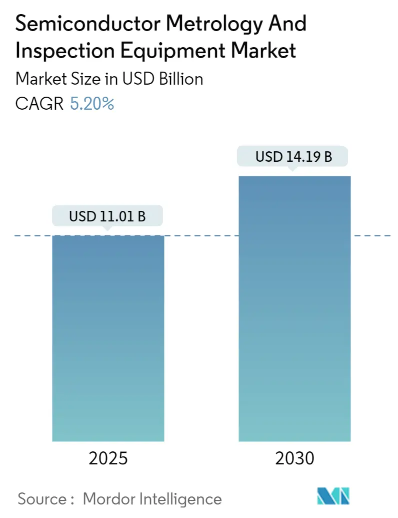
| Market Size (2025) | USD 11.01 Billion |
| Market Size (2030) | USD 14.19 Billion |
| Growth Rate (2025 - 2030) | 5.20% CAGR |
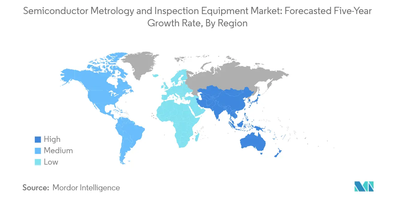
| Fastest Growing Market | Asia Pacific |
| Largest Market | Asia Pacific |
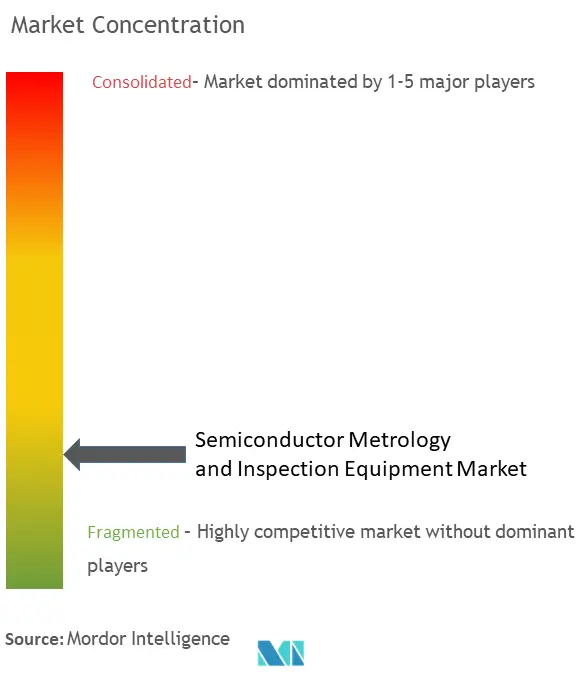
| Market Concentration | Low |
Major Players
*Disclaimer: Major Players sorted in no particular order Image © Mordor Intelligence. Reuse requires attribution under CC BY 4.0. |
|
Semiconductor Metrology and Inspection Equipment Market Analysis
The Semiconductor Metrology And Inspection Equipment Market size is estimated at USD 11.01 billion in 2025, and is expected to reach USD 14.19 billion by 2030, at a CAGR of 5.2% during the forecast period (2025-2030).
The semiconductor manufacturing equipment industry operates within a complex manufacturing ecosystem where precision and quality control are paramount. The manufacturing process of semiconductor wafers involves approximately 400 to 600 steps, which can be completed within one to two months, making early detection of defects crucial for preventing wastage in subsequent steps. This intricate process requires sophisticated semiconductor metrology and semiconductor inspection equipment procedures implemented at critical junctures to guarantee specific yields. The industry's landscape is further shaped by ongoing geopolitical tensions, particularly the US-China trade dispute, which has resulted in restrictions on China's access to advanced semiconductor manufacturing equipment, creating significant supply chain disruptions and market uncertainties.
Technological advancement in semiconductor manufacturing continues to push the boundaries of innovation, with companies making significant strides in process node development. In June 2022, Samsung Electronics initiated the production of its 3-nanometer process node applying Gate-All-Around (GAA) transistor architecture, marking a significant milestone in semiconductor manufacturing capabilities. The industry's focus on miniaturization and enhanced performance has led to the development of more sophisticated semiconductor inspection equipment and semiconductor metrology solutions. This evolution is particularly evident in the increasing adoption of artificial intelligence and machine learning technologies for defect detection and classification.
The rollout of 5G technology is creating new demands for semiconductor manufacturing equipment. According to GSMA projections, 5G mobile broadband connections are expected to reach 1.1 billion by 2025, with network coverage extending to 34% of the global population. This expansion is driving the need for more advanced semiconductor manufacturing processes and, consequently, more sophisticated semiconductor process control solutions. The industry is responding with innovations in measurement and inspection technologies to meet the stringent requirements of 5G semiconductor components.
Recent industry developments highlight the continuous evolution of metrology solutions. In January 2023, k-Space Associates introduced its latest thin film metrology tool, the kSA XRF (X-ray fluorescence), specifically designed for accurate semiconductor measurement of films that cannot be reliably measured using optical methods. This innovation demonstrates the industry's response to emerging challenges in semiconductor manufacturing, particularly in measuring semiconductor and dielectric layers on various substrates. The market is witnessing increased collaboration between vendors to develop advanced multifunction inspection platforms, addressing the growing complexity of semiconductor manufacturing processes while maintaining high precision and efficiency standards.
Semiconductor Metrology and Inspection Equipment Market Market Trends
Increasing Demand for High-Performance, Low-Cost Semiconductors
The semiconductor industry is experiencing unprecedented demand for high-performance, low-cost semiconductor materials, primarily driven by the rapid advancement of wireless technologies, artificial intelligence, and emerging applications across various sectors. This trend is particularly evident in the deployment of 5G networks, where, according to the Ericsson Mobility Report 2022, 5G subscriptions are projected to reach 4.4 billion globally by 2027, representing nearly half of all mobile subscriptions. The demand for enhanced performance is further illustrated by significant technological breakthroughs, such as Samsung Electronics' initiation of 3-nanometer process node production in 2023, applying Gate-All-Around (GAA) transistor architecture to achieve superior performance while maintaining cost efficiency.
The push for miniaturization and improved performance continues to drive innovation in semiconductor manufacturing processes. This is exemplified by breakthrough developments such as IBM's 2-nanometer chip technology, which promises to deliver 45% higher performance or 75% lower energy consumption compared to advanced 7nm node chips. The industry's focus on high-performance computing is further reinforced by regional adoption patterns, with projections indicating that by 2027, 90% of North American subscriptions will be 5G, followed by 82% in Western Europe and 80% in the Gulf Cooperation Council regions. These advancements in semiconductor technology are essential for supporting the growing demands of artificial intelligence, high-performance computing, and other emerging technologies that require increasingly sophisticated and efficient semiconductor solutions. Furthermore, the role of semiconductor testing and semiconductor quality control becomes critical in ensuring the reliability and efficiency of these advanced technologies.
Increasing Demand for Semiconductor Wafers in Consumer Electronics
The consumer electronics sector is driving substantial demand for semiconductor wafers, with applications ranging from smartphones and tablets to wearable devices and smart home technology. According to recent industry data from 2023, global silicon wafer shipments reached 12,602 million square inches, reflecting the intensive use of semiconductors in consumer electronic devices. The demand is particularly evident in the growing adoption of fast-charging technologies across various device categories, where manufacturers like OPPO, OnePlus, Motorola, Samsung, and Apple are incorporating advanced semiconductor solutions in their power adapters to meet consumer expectations for faster charging capabilities while maintaining device safety and efficiency.
The proliferation of Internet of Things (IoT) devices and wearable technology is further accelerating the demand for semiconductor wafers in consumer electronics. This trend is supported by the increasing integration of computational power and additional sensors in traditionally simple devices, requiring more sophisticated semiconductor solutions. The industry is witnessing a significant shift toward miniaturized chips and advanced packaging technologies to accommodate the growing demand for lightweight electronic devices while maintaining high performance and low power consumption. This evolution is particularly notable in the wearables segment, where manufacturers are developing more efficient processors that can deliver enhanced functionality within increasingly compact form factors, driving the need for advanced semiconductor wafer technologies and sophisticated inspection processes to ensure quality and reliability. The importance of the semiconductor manufacturing equipment market and semiconductor quality assurance is underscored in this context, as they play a pivotal role in maintaining the standards required for these sophisticated devices. Additionally, semiconductor failure analysis is crucial in identifying and mitigating potential issues in these advanced applications.
Segment Analysis: By Type
Other Process Control Systems Segment in Semiconductor Metrology and Inspection Equipment Market
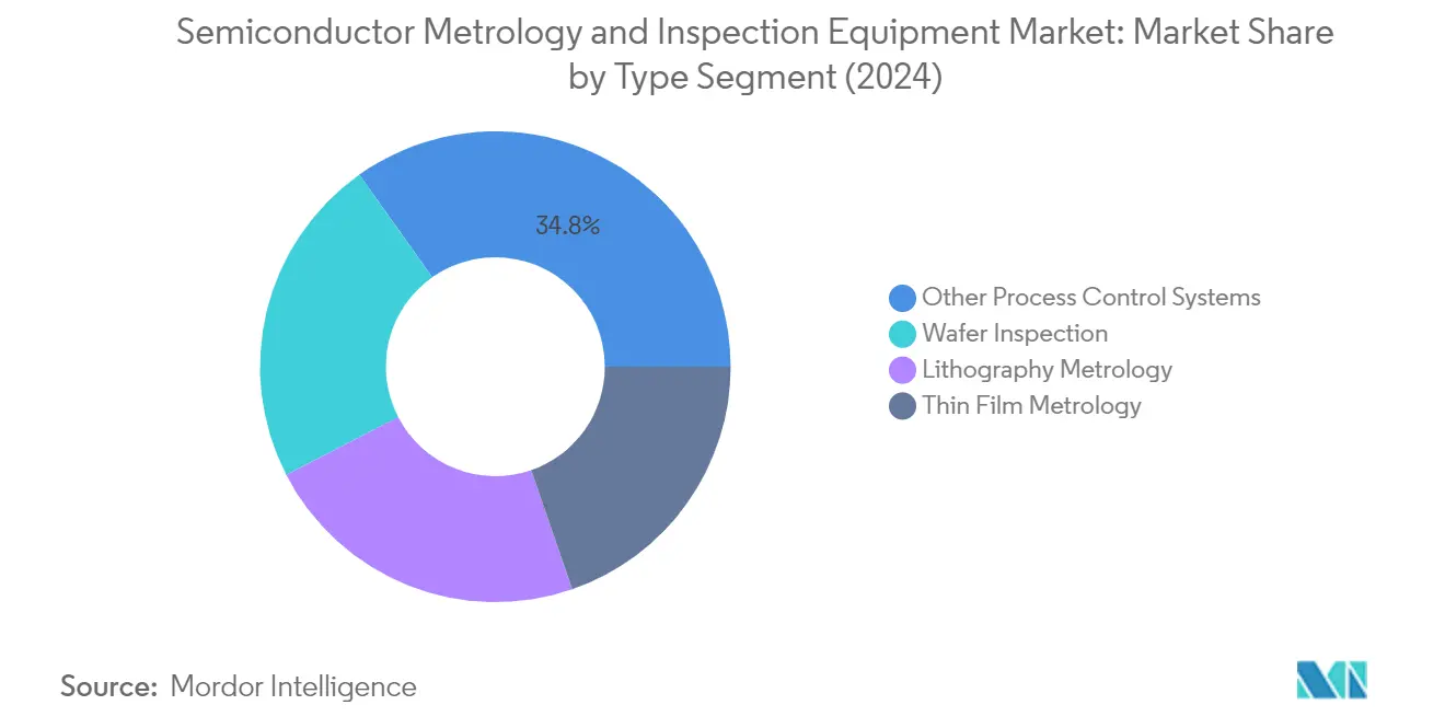
The Other Process Control Systems segment dominates the Semiconductor Metrology and Inspection Equipment market, holding approximately 35% market share in 2024. This segment encompasses critical non-lithographic inspection techniques capable of detecting various errors, including mask CDU/PPE, wafer shape, process overlay, etch, and deposition defects. The segment's prominence is driven by the increasing complexity of semiconductor manufacturing processes and the growing demand for comprehensive quality control. Major semiconductor manufacturers are increasingly investing in advanced process control systems to maintain high yields and quality standards in their fabrication facilities. The integration of artificial intelligence and machine learning capabilities in these systems has further enhanced their effectiveness in detecting and classifying defects, making them indispensable in modern semiconductor manufacturing.
Wafer Inspection Segment in Semiconductor Metrology and Inspection Equipment Market
The Wafer Inspection segment is emerging as the fastest-growing segment in the market, projected to grow at approximately 6% during 2024-2029. This growth is primarily driven by the increasing demand for three-dimensional integrated circuits used in miniature semiconductor devices such as memory cards, smartphones, and various computing devices. The segment's rapid expansion is further supported by the growing adoption of 300mm wafers in LED applications and the rising need for efficient temperature control in thin wafers. The implementation of automated semiconductor inspection systems, enhanced by artificial intelligence and machine learning capabilities, is revolutionizing wafer inspection processes, enabling higher throughput and more accurate defect detection. The segment's growth is also bolstered by the increasing focus on quality control in semiconductor manufacturing and the rising demand for advanced packaging solutions.
Remaining Segments in Semiconductor Metrology and Inspection Equipment Market
The Lithography Metrology and Thin Film Metrology segments play crucial roles in the semiconductor manufacturing ecosystem. Lithography Metrology equipment is essential for controlling and optimizing semiconductor manufacturing processes, particularly in pattern measurement and imaging of wafer designs. The segment's importance is amplified by the industry's continuous push toward smaller node sizes and more complex circuit patterns. Meanwhile, Thin Film Metrology provides vital capabilities in monitoring metrological parameters such as thickness, sensitivity, and composition in semiconductor devices and nanodevices. These segments are particularly significant in advanced applications such as 5G communications, artificial intelligence processors, and next-generation memory devices. The use of optical inspection equipment in these segments is crucial for ensuring precision and accuracy in semiconductor defect inspection.
Semiconductor Metrology And Inspection Equipment Market Geography Segment Analysis
Semiconductor Metrology and Inspection Equipment Market in North America
The North American semiconductor manufacturing equipment market continues to maintain a strong position in key future technologies, including artificial intelligence (AI), quantum computing, and sophisticated wireless networks like 5G. With approximately 18% market share in 2024, North America represents a significant portion of the global market. The region's strength is primarily driven by substantial investments in state-of-the-art semiconductor inspection equipment and manufacturing facilities. The U.S. government's push for semiconductor independence has led to an increased focus on domestic manufacturing capabilities and quality control systems. The surge in demand for advanced technologies, such as machine-to-machine communication, connected cars, and artificial intelligence, has created significant opportunities for semiconductor metrology and inspection equipment vendors. The region's growing electric vehicle market and expanding Internet of Things (IoT) ecosystem have further accelerated the need for sophisticated inspection and metrology solutions. Additionally, the increasing adoption of wearables for fitness and medical applications has created new demand vectors for wafer inspection equipment, while the rapid advancement in chip manufacturing technologies continues to drive innovation in metrology solutions.
Semiconductor Metrology and Inspection Equipment Market in Europe
Europe has established itself as a crucial hub for semiconductor inspection equipment, demonstrating approximately 5% growth from 2019 to 2024. The region's market is characterized by strong technological innovation and increasing adoption of advanced semiconductor technologies across various industries. European countries have been actively investing in semiconductor manufacturing capabilities, with particular emphasis on quality control and inspection systems. The region's strong automotive and industrial sectors continue to drive demand for high-precision metrology equipment. The push towards renewable energy solutions, particularly in offshore wind power generation, has created additional demand for power semiconductor inspection systems. European manufacturers have been focusing on developing advanced inspection technologies for next-generation semiconductor devices, particularly in areas such as 3D integration and advanced packaging. The region's commitment to digital transformation across industries has further accelerated the need for sophisticated metrology and inspection solutions. The presence of major research institutions and technology centers has also contributed to continuous innovation in measurement and inspection methodologies.
Semiconductor Metrology and Inspection Equipment Market in Asia-Pacific
The Asia-Pacific region dominates the global semiconductor manufacturing equipment market, with projections indicating approximately 6% growth from 2024 to 2029. The region's market leadership is built on its robust semiconductor manufacturing ecosystem, particularly in countries like China, Taiwan, South Korea, and Japan. The continuous expansion of semiconductor fabrication facilities in these countries has created sustained demand for advanced inspection and metrology solutions. The region's focus on developing domestic semiconductor capabilities has led to increased investments in quality control and inspection systems. The growing adoption of advanced technologies such as 5G, artificial intelligence, and the Internet of Things has further accelerated the need for sophisticated measurement and inspection equipment. Local manufacturers have been actively developing innovative inspection solutions to address the increasing complexity of semiconductor devices. The region's strong consumer electronics manufacturing base continues to drive demand for high-precision metrology equipment, while the growing automotive electronics sector has created additional opportunities for inspection system providers.
Semiconductor Metrology and Inspection Equipment Market in Rest of the World
The Rest of the World region, encompassing Latin America, the Middle East, and Africa, represents an emerging market for semiconductor metrology and inspection equipment. The region is witnessing growing opportunities driven by increasing investments in semiconductor manufacturing capabilities and quality control systems. Countries across Latin America, particularly Brazil and Mexico, are showing increased interest in developing domestic semiconductor capabilities, creating new opportunities for metrology and inspection equipment providers. The Middle East region's focus on diversifying its economy has led to investments in high-technology manufacturing, including semiconductor production facilities. The growing adoption of renewable energy solutions across these regions has created additional demand for power semiconductor inspection systems. The increasing consumption of consumer electronic devices has also contributed to the growth of the market. The region's relatively lower operational costs have attracted both local and international manufacturers, leading to increased demand for inspection and metrology solutions. The development of new manufacturing facilities and the emphasis on quality control have created sustained demand for advanced inspection equipment.
Semiconductor Metrology and Inspection Equipment Industry Overview
Top Companies in Semiconductor Metrology and Inspection Equipment Market
The semiconductor inspection equipment companies market is characterized by intense innovation and strategic developments from leading players like KLA Corporation, Applied Materials, Hitachi High-Tech, ASML Holding, and Nova Measuring Instruments. Companies are heavily investing in research and development to enhance their product portfolios, particularly focusing on advanced inspection systems incorporating AI and machine learning capabilities. The industry witnesses continuous product launches targeting emerging applications in 3D IC, advanced packaging, and EUV lithography inspection. Operational agility is demonstrated through flexible manufacturing approaches, with many players adopting outsourcing strategies for non-core components while maintaining control over critical technologies. Strategic moves include establishing regional research centers, forming university partnerships, and expanding manufacturing facilities, particularly in Asia-Pacific where semiconductor manufacturing is concentrated. Companies are also pursuing vertical integration through acquisitions to strengthen their technological capabilities and market presence.
Market Dominated by Global Technology Conglomerates
The semiconductor inspection equipment market exhibits a high degree of consolidation, with a few global technology conglomerates controlling significant market share. These dominant players leverage their extensive research capabilities, established distribution networks, and long-standing relationships with semiconductor manufacturers to maintain their market positions. The market structure favors established players due to high entry barriers, including substantial capital requirements, complex technological expertise, and the need for strong intellectual property portfolios. Local players typically focus on specific niches or serve as suppliers to larger companies, while global leaders offer comprehensive solution portfolios spanning multiple inspection and metrology technologies.
The industry has witnessed strategic consolidation through mergers and acquisitions, aimed at expanding technological capabilities and geographic reach. Companies are particularly interested in acquiring specialized technology firms that bring innovative inspection and metrology solutions or complement existing product lines. The trend toward consolidation is driven by the need to achieve economies of scale, enhance research and development capabilities, and offer integrated solutions to customers. Market leaders are also establishing strategic partnerships with research institutions and technology providers to accelerate innovation and maintain competitive advantages.
Innovation and Customer Relations Drive Success
Success in the semiconductor testing industry increasingly depends on maintaining technological leadership while building strong customer relationships. Incumbent companies must continuously invest in research and development to address emerging challenges in semiconductor manufacturing, particularly in areas like 3D integration, advanced packaging, and sub-nanometer inspection capabilities. Market leaders are focusing on developing comprehensive solution portfolios that combine hardware, software, and services to create higher entry barriers and increase customer switching costs. Companies are also emphasizing the development of automated, AI-driven inspection systems to address the growing complexity of semiconductor manufacturing processes.
For contenders seeking to gain market share, specialization in emerging technology niches and strong customer support capabilities are crucial success factors. The high concentration of end-users in the semiconductor manufacturing industry makes relationship management and technical support capabilities critical for market success. While substitution risk is relatively low due to the specialized nature of inspection and metrology equipment, companies must stay ahead of technological changes to maintain their market positions. Regulatory compliance, particularly regarding export controls and intellectual property protection, continues to influence market dynamics and company strategies. Future success will depend on balancing innovation with operational efficiency while maintaining strong relationships with key semiconductor manufacturers.
Semiconductor Metrology and Inspection Equipment Market Major Players
-
KLA Corporation
-
Applied Materials Inc.
-
Onto Innovation Inc.
-
Thermo Fisher Scientific Inc.
-
Hitachi Hi-Technologies Corporation (Hitachi Limited)
- *Disclaimer: Major Players sorted in no particular order
Semiconductor Metrology and Inspection Equipment Market Recent Developments
- March 2024 - The LS9300AD, a novel system developed by Hitachi High-Tech Corporation, was introduced to examine non-patterned wafer surfaces for particles and defects on both the front and back sides. This advanced system not only utilizes the traditional dark-field laser scattering technique to detect foreign materials and defects but also incorporates a new inspection function called DIC (differential interference contrast). This function allows for the identification of irregular defects, including those that are shallow and have a low aspect ratio. Furthermore, the LS9300AD features the wafer edge grip method and rotating stage, which are currently employed in conventional products, thereby facilitating comprehensive inspection of both sides of the wafer.
- September 2023 - Nagoya University's startup, Photoelectron Soul Inc., announced the successful fundraising of JPY 730 million. PeS finalized an exclusive distribution agreement with USHIO for its innovative semiconductor photocathode e-beam generation systems, which are integrated into e-beam semiconductor wafer pattern inspection tools. The growing adoption of e-beam wafer inspection systems by semiconductor manufacturers is propelling the rising demand for these systems. This is because of their capability to offer high-quality inspection, leading to lucrative opportunities for e-beam wafer inspection technology.
Semiconductor Metrology and Inspection Equipment Industry Segmentation
Semiconductor metrology and inspection are essential for the management of the semiconductor manufacturing process. There are hundreds of steps in the semiconductor wafer manufacturing process that are undertaken in months. Hence, metrology and inspection processes are established at critical points of the semiconductor manufacturing process chain to maintain a specific yield.
The semiconductor metrology and inspection equipment market is segmented by type and geography. By type, the market is segmented into lithography metrology, wafer inspection, and thin film metrology. By lithography metrology, the segment is divided into overlay, dimension equipment, mask inspection, and metrology. By geography, the market is divided into North America, Europe, Asia-Pacific, and Rest of the World. The market size and forecasts are provided in terms of value (USD) for all the above segments.
| By Type | Lithography Metrology | Overlay |
| Dimension Equipment | ||
| Mask Inspection and Metrology | ||
| Wafer Inspection | ||
| Thin Film Metrology | ||
| Other Process Control Systems | ||
| By Geography | North America | |
| Europe | ||
| Asia-Pacific | ||
| Rest of the World |
| Lithography Metrology | Overlay |
| Dimension Equipment | |
| Mask Inspection and Metrology | |
| Wafer Inspection | |
| Thin Film Metrology | |
| Other Process Control Systems |
| North America |
| Europe |
| Asia-Pacific |
| Rest of the World |
Semiconductor Metrology & Inspection Equipment Market Research FAQs
How big is the Semiconductor Metrology And Inspection Equipment Market?
The Semiconductor Metrology And Inspection Equipment Market size is expected to reach USD 11.01 billion in 2025 and grow at a CAGR of 5.20% to reach USD 14.19 billion by 2030.
What is the current Semiconductor Metrology And Inspection Equipment Market size?
In 2025, the Semiconductor Metrology And Inspection Equipment Market size is expected to reach USD 11.01 billion.
Who are the key players in Semiconductor Metrology And Inspection Equipment Market?
KLA Corporation, Applied Materials Inc., Onto Innovation Inc., Thermo Fisher Scientific Inc. and Hitachi Hi-Technologies Corporation (Hitachi Limited) are the major companies operating in the Semiconductor Metrology And Inspection Equipment Market.
Which is the fastest growing region in Semiconductor Metrology And Inspection Equipment Market?
Asia Pacific is estimated to grow at the highest CAGR over the forecast period (2025-2030).
Which region has the biggest share in Semiconductor Metrology And Inspection Equipment Market?
In 2025, the Asia Pacific accounts for the largest market share in Semiconductor Metrology And Inspection Equipment Market.
What years does this Semiconductor Metrology And Inspection Equipment Market cover, and what was the market size in 2024?
In 2024, the Semiconductor Metrology And Inspection Equipment Market size was estimated at USD 10.44 billion. The report covers the Semiconductor Metrology And Inspection Equipment Market historical market size for years: 2019, 2020, 2021, 2022, 2023 and 2024. The report also forecasts the Semiconductor Metrology And Inspection Equipment Market size for years: 2025, 2026, 2027, 2028, 2029 and 2030.
Page last updated on: June 16, 2024

