Semiconductor Metrology And Inspection Equipment Market Size and Share
Market Overview
| Study Period | 2019 - 2030 |
|---|---|
| Market Size (2025) | USD 13.03 Billion |
| Market Size (2030) | USD 16.95 Billion |
| Growth Rate (2025 - 2030) | 5.40% CAGR |
| Fastest Growing Market | Asia Pacific |
| Largest Market | Asia Pacific |
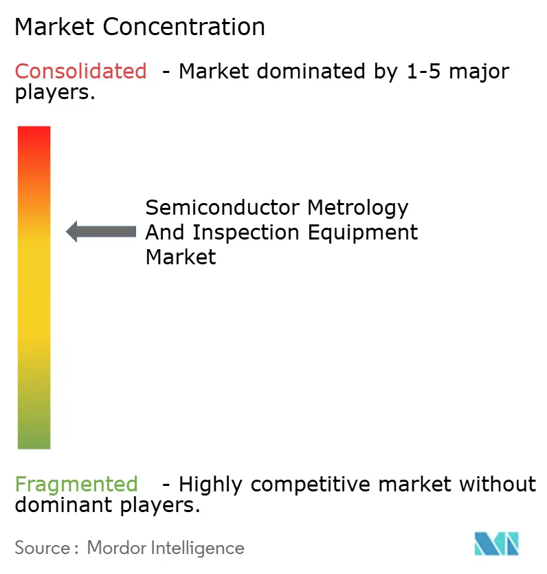
| Market Concentration | Medium |
Major Players *Disclaimer: Major Players sorted in no particular order Image © Mordor Intelligence. Reuse requires attribution under CC BY 4.0. | |
Semiconductor Metrology And Inspection Equipment Market Analysis by Mordor Intelligence
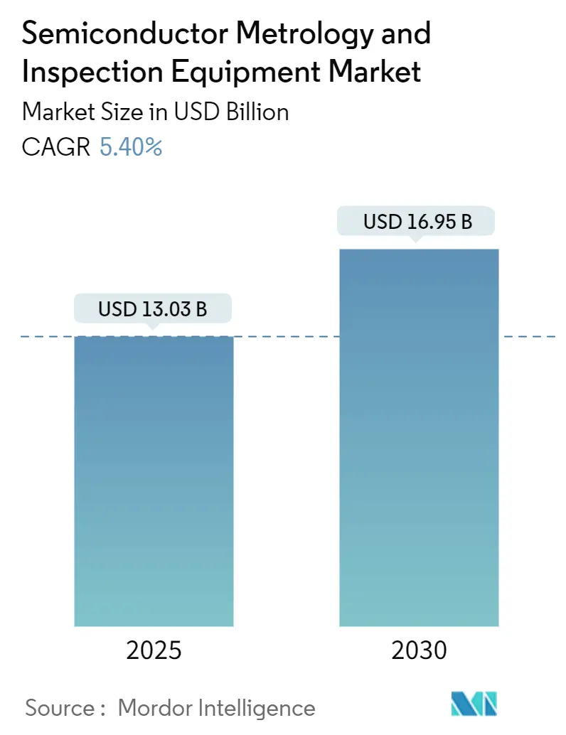
The semiconductor metrology and inspection system market size stands at USD 13.03 billion in 2025 and is projected to reach USD 16.95 billion in 2030, reflecting a 5.4% CAGR for the period 2025-2030. These advances trace the sector’s shift from capacity-driven expansion toward precision-centric investment, where sub-nanometer accuracy replaces throughput as the core value driver. Momentum stems from three forces: the need to control critical dimensions below 7 nm, the vertical scaling of 3D NAND memories beyond 200 layers, and the growing adoption of sovereign manufacturing programs that diversify geographic production. Foundry operators now allocate 15-20% of their capital expenditure to process-control equipment, underscoring yield optimization as the new strategic imperative. Competitive differentiation hinges on AI-enhanced analytics, where machine-learning algorithms reduce inspection time and enable real-time process adjustments.[1]Source: KLA Corporation, “Metrology Tools and Defect Inspection Instruments,” kla.com Supply-chain pressure for helium and specialty gases, combined with a scarcity of skilled metrology engineers, tempers near-term expansion while also accelerating the development of integrated solutions that lock in consumables and training services.[2]Source: SEMI, “Global Total Semiconductor Equipment Sales Forecast,” semi.org
Key Report Takeaways
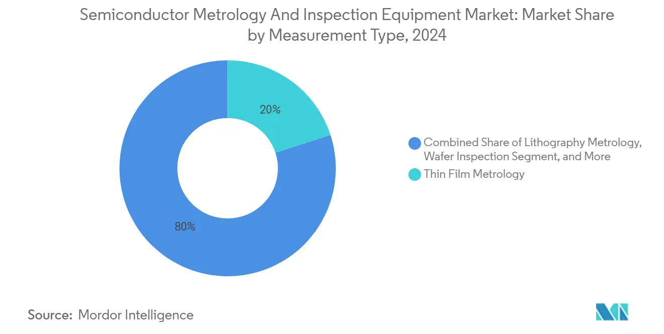
- By measurement type, thin film metrology led the semiconductor metrology and inspection system market, accounting for a 20% revenue share in 2024. The segment is set to expand at a 6.2% CAGR through 2030.
- By technology node, devices at less than 3nm are projected to record the fastest 9.25% CAGR to 2030 within the semiconductor metrology and inspection system market size.
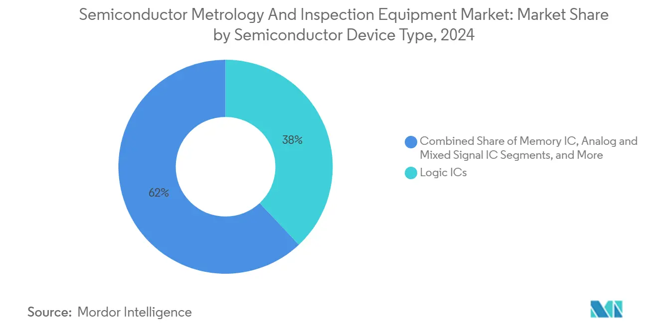
- By semiconductor device type, logic ICs accounted for 38% of the semiconductor metrology and inspection system market share in 2024; memory IC applications are projected to advance at an 8.5% CAGR through 2030.
- By end-use industry, computing and data center applications are forecast to expand at a 7.1% CAGR, the highest among all end uses.
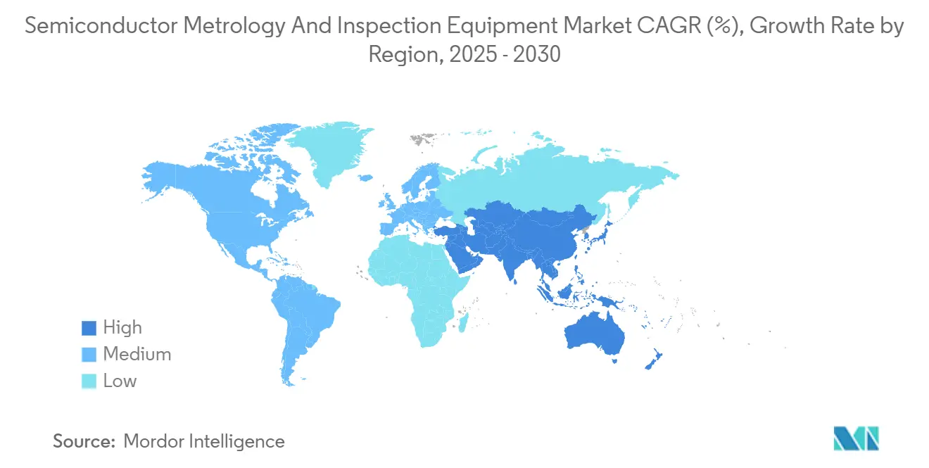
- By geography, the Asia Pacific accounted for the largest market share and is poised to grow at a 7.65% CAGR, outpacing all other regions.
Global Semiconductor Metrology And Inspection Equipment Market Trends and Insights
Drivers Impact Analysis*
| Driver | (~ ) % Impact on CAGR Forecast | Geographic Relevance | Impact Timeline |
|---|---|---|---|
| Rising demand for sub-7 nm node accuracy | +1.8% | Global, led by Taiwan and Korea | Medium term (2-4 years) |
| Growth in 3D NAND and advanced memory production | +1.2% | APAC core, spill-over to North America | Long term (≥ 4 years) |
| Expansion of foundry capacities in APAC | +0.9% | APAC, with emerging Middle East presence | Medium term (2-4 years) |
| Adoption of hybrid bonding metrology | +0.7% | Global, concentrated in advanced packaging hubs | Long term (≥ 4 years) |
| In-situ AI analytics reducing tool downtime | +0.4% | Global, early adoption in leading fabs | Short term (≤ 2 years) |
| Sustainability mandates driving low-defect yields | +0.2% | Europe and North America regulatory focus | Long term (≥ 4 years) |
| Source: Mordor Intelligence | |||
Rising Demand for Sub-7 nm Node Accuracy
Below 7 nm, gate-all-around transistors introduce three-dimensional structures that demand measurement precision of 0.5 nm for critical dimensions. Optical methods reach physical limits, prompting the development of hybrid e-beam and X-ray inspection platforms that can resolve high-aspect-ratio features. Intel’s purchase of an entire 2024 batch of High-NA EUV scanners underlines the premium placed on advanced metrology for process leadership. Overlay accuracy has tightened to sub-nanometer tolerances, making integrated alignment metrology essential to sustain electrical performance across multi-patterned layers.
Growth in 3D NAND and Advanced Memory Production
Vertical flash devices now exceed 200 layers, forcing thin-film metrology tools to measure individual layers thinner than 10 nm while maintaining repeatability of less than 0.1% over 300 mm wafers. Samsung’s roadmap to 300-layer stacks accentuates the need for inline control of etch depth and stack height uniformity.[3]Source: Samsung Electronics, “300-Layer 3D NAND Development Roadmap,” samsung.com High-bandwidth memory incorporates through-silicon-via alignment checks and thermal-interface uniformity into routine inspection, thereby broadening the scope of metrology spend within memory fabs.
Expansion of Foundry Capacities in Asia-Pacific
Capacity additions across Taiwan, South Korea, and China remain central, yet sovereign projects in the UAE and Saudi Arabia bring fresh growth to the semiconductor metrology and inspection system market.[4]Source: UAE Government Media Office, “UAE Semiconductor Strategy,” uaegov.aeThe distributed model requires tool vendors to replicate service infrastructure regionally, while ensuring consistency across different fabrics. As a result, vendors bundle equipment with remote diagnostics and multilingual training modules, shortening ramp-up time for new fabs.
Adoption of Hybrid Bonding Metrology
Hybrid bonding, pivotal for chiplet architectures and high-bandwidth memory, demands surface planarity within 10 nm and copper pad height uniformity tighter than 50 nm. New tools combine optical interferometry, white-light profilometry, and X-ray tomography to verify bond quality pre-stack. Veeco’s collaboration with IBM on wet-process steps demonstrates how equipment firms integrate front-end and packaging metrology expertise to gain a competitive edge.
Restraints Impact Analysis*
| Restraint | (~) % Impact on CAGR Forecast | Geographic Relevance | Impact Timeline |
|---|---|---|---|
| Shortage of skilled metrology engineers | -0.8% | Global, severe in APAC expansion regions | Long term (≥ 4 years) |
| Supply chain risks for helium and specialty gases | -0.5% | Global, concentrated risk points | Short term (≤ 2 years) |
| Data-security concerns in cloud-based inspection | -0.3% | Regulated industries and defense applications | Medium term (2-4 years) |
| High capital expenditure of e-beam and EUV tools | -1.1% | Global, acute in emerging markets | Medium term (2-4 years) |
| Source: Mordor Intelligence | |||
High Capital Expenditure of E-beam and EUV Tools
Unit prices exceed approximately USD 15 million for advanced e-beam systems and approximately USD 25 million for EUV-capable metrology equipment. Smaller foundries hesitate to commit, delaying adoption despite clear technical need. Financing packages that bundle hardware, software, service, and helium supply contracts emerge as risk-sharing models to broaden access.
Shortage of Skilled Metrology Engineers
AI-enabled inspection platforms require expertise that blends optics, materials science, and machine learning. Universities lag in producing specialists, leaving fabs with prolonged hiring cycles that slow tool qualification. Industry consortia fund accelerated certification programs; yet, the gap persists, nudging vendors to offer turnkey solutions with embedded remote support.
*Our forecasts treat driver/restraint impacts as directional, not additive. The impact forecasts reflect baseline growth, mix effects, and variable interactions.
Segment Analysis
By Measurement Type: Thin-Film Dominance in 3D Architectures
Thin-film metrology is expected to contribute approximately 20% to the semiconductor metrology and inspection system market size in 2025 and is projected to grow at a 6.2% CAGR through 2030. Stack-height control for 3D NAND and conformality checks for atomic-layer-deposited films dominate tool orders. Lithography metrology remains the revenue leader, thanks to overlay and critical-dimension modules embedded in every litho cell. The shift to hybrid bonding also amplifies demand for high-resolution surface-profiling tools. AI classification reduces recipe setup time by 20%, improving fab throughput.
Wafer-inspection platforms integrate multi-spectral lighting and e-beam modules on shared stages, cutting queue times and enabling cross-modality correlation. Cognex’s AI-infused 3D vision launch in 2024 signaled the migration of machine-vision vendors into front-end fabs, expanding competitive boundaries.Other process-control systems, including advanced packaging inspection, post-chemical-mechanical-polish metrology, and compound-semiconductor measurement, form a high-growth but smaller niche that captures fabs exploring SiC and GaN power devices.


By Technology Node: Sub-3 nm Complexity Drives Premium Growth
The sub-3 nm category commands a 9.25% CAGR, the fastest in the semiconductor metrology and inspection system market, driven by gate-all-around transistors and backside power delivery, which magnify the complexity of three-dimensional measurement. The 10-7 nm band still absorbs sizable orders from mobile SoC lines, while the 14-22 nm tranche stays important for automotive safety chips. ASML’s High-NA EUV scanners, with an optical resolution of 8 nm, necessitate parallel upgrades in overlay metrology, capable of achieving a 0.3 nm registration error, underscoring the tight coupling between lithography and inspection.
Nodes with diameters of 28 nm or greater carry cost-sensitive consumer and IoT parts; in these cases, fabs utilize remanufactured legacy metrology tools to minimize capital expenditures. Yet even mature nodes incorporate AI analytics to enhance yield without necessitating drastic equipment refreshes, illustrating the pervasive influence of data science across all geometries.
By Semiconductor Device Type: Memory IC Applications Lead Growth
Memory lines are expected to contribute significantly to the semiconductor metrology and inspection system market in 2025, growing at an 8.5% CAGR, outpacing logic as HBM stacks and high-layer 3D NAND require structural verification. Logic retains the single-largest revenue slice on sheer wafer starts for CPUs and GPUs. Analog-mixed signal chips utilize optical scatterometry for measuring thick metal layers, whereas power devices employ X-ray systems to detect voids in copper clip attachments.
Optoelectronics are expanding steadily due to the demand for silicon photonics in cloud data-center interconnects, which require sub-50 nm waveguide width control. Each device class thus maintains a unique metrology profile, compelling suppliers to diversify toolsets to cover disparate measurement targets.
By End-Use Industry: Computing Centers Drive AI-Era Demand
Hyperscaler data center spending is increasing significantly from 2024 to 2026, driving computing and data center applications at a 7.1% CAGR in the semiconductor metrology and inspection system market. Consumer electronics still deliver the highest wafer volumes but show flatter growth as smartphone refresh cycles lengthen. Automotive demand accelerates with the penetration of ADAS, prompting stringent zero-defect goals.
Industrial IoT generates steady revenue, particularly for power and mixed-signal chips that power factory-automation controllers. The healthcare and aerospace segments pay premium prices for radiation-hardened or biocompatible devices, thereby elongating qualification cycles while offering robust margins for specialized metrology tools.
Geography Analysis
The semiconductor metrology and inspection system market in the Asia Pacific region was dominated by Taiwan, South Korea, and China, which collectively retained a majority share. Foundry operators allocate up to 20% of their capital budgets to process control, reflecting a strategic shift toward yield rather than pure output, making the region the fastest-growing, with a 7.65% CAGR. North America follows with coordinated CHIPS-Act incentives bolstering fab construction in Arizona, Texas, and Ohio.
The Middle East, although starting from a small base, achieves a significant CAGR as the UAE and Saudi Arabia pursue technology-sovereignty agendas that span design to back-end testing. Europe maintains modest yet stable growth tied to automotive semiconductors, aided by carbon-neutral mandates that value measurement-driven yield improvement. South America and Africa remain nascent but attract pilot lines for power devices and assembly operations, creating long-tail prospects for low-footprint metrology platforms.

Competitive Landscape
Incumbents KLA, Applied Materials, and ASML control a majority of the semiconductor metrology and inspection system market, leveraging decades of process-control domain knowledge and integrated software analytics to secure customer loyalty. KLA reported significant year-over-year growth in Q1 2025, driven by demand for broadband plasma inspection and optical scatterometry tools. Applied Materials deepened its position by taking a majority stake in Kokusai Electric, aligning batch furnace expertise with metrology services to deliver turnkey process cells. ASML’s High-NA EUV roadmap anchors its YieldStar overlay platform, ensuring tight coupling between exposure and inspection. Start-ups target gaps in hybrid bonding, backside power delivery, and compound-semiconductor inspection, competing through agility and niche specialization. Vendors are increasingly bundling AI-enabled software subscriptions, predictive maintenance service contracts, and supply chain logistics to create multi-year revenue streams beyond initial tool sales.
Patent filings in AI-assisted defect classification increased in 2024, indicating that algorithms, rather than optics alone, will underpin next-generation competitiveness. Industry bodies such as IEEE and SEMI push standards for defect taxonomy and data formats, influencing vendor roadmaps and facilitating multi-vendor data exchange, an essential prerequisite for cross-fab benchmarking in distributed manufacturing networks.
Semiconductor Metrology And Inspection Equipment Industry Leaders
KLA Corporation
Applied Materials Inc.
Onto Innovation Inc.
Thermo Fisher Scientific Inc.
Hitachi Hi-Technologies Corporation (Hitachi Limited)
- *Disclaimer: Major Players sorted in no particular order

Recent Industry Developments
- August 2025: SkyWater Technology acquired Infineon’s Austin 200 mm fab, adding 65-130 nm capacity and creating 600 jobs.
- July 2025: Applied Materials became the largest shareholder of Kokusai Electric after KKR’s partial divestiture, expanding process-control reach.
- June 2025: Entegris secured up to USD 75 million CHIPS-Act funding to build a Colorado Springs facility for FOUPs and filtration products.
- April 2025: ASML debuted the TWINSCAN EXE High-NA EUV scanner with 8 nm resolution and 40% higher imaging contrast.


Global Semiconductor Metrology And Inspection Equipment Market Report Scope
Semiconductor metrology and inspection are crucial for managing the semiconductor manufacturing process. There are hundreds of steps in the semiconductor wafer manufacturing process that are undertaken in months. Hence, metrology and inspection processes are established at critical points of the semiconductor manufacturing process chain to maintain a specific yield.
The Semiconductor Metrology and Inspection System Market Report is Segmented by Measurement Type (Lithography Metrology, Wafer Inspection, Thin Film Metrology, and Other Process Control Systems), Technology Node (Less Than 3 Nm, 3 Nm, 5 Nm, 7 Nm, 14/16 nm, 28 nm, and Greater Than 28 nm), Semiconductor Device Type (Logic IC, Memory IC, Analog and Mixed Signal IC, Power Devices, and Optoelectronics), End-Use Industry (Consumer Electronics, Computing and Data Centers, Automotive and Transportation, Industrial, Healthcare and Life Sciences, Aerospace and Defense, and Other End User Industries), and Geography (North America, South America, Asia-Pacific, Europe, and Middle East and Africa). The Market Forecasts are Provided in Terms of Value (USD).
| Lithography Metrology | Overlay |
| Dimension Equipment | |
| Mask Inspection and Metrology | |
| Wafer Inspection | |
| Thin Film Metrology | |
| Other Process Control Systems |
| Less Than 3 nm |
| 3 nm |
| 5 nm |
| 7 nm |
| 14/16 nm |
| 28 nm |
| Greater Than 28 nm |
| Logic IC |
| Memory IC |
| Analog and Mixed Signal IC |
| Power Devices |
| Optoelectronics |
| Consumer Electronics |
| Computing and Data Centers |
| Automotive and Transportation |
| Industrial |
| Healthcare and Life Sciences |
| Aerospace and Defense |
| Other End User Industries |
| North America | United States | |
| Canada | ||
| Mexico | ||
| Europe | Germany | |
| United Kingdom | ||
| France | ||
| Italy | ||
| Rest of Europe | ||
| Asia-Pacific | China | |
| Japan | ||
| South Korea | ||
| India | ||
| Rest of Asia-Pacific | ||
| South America | Brazil | |
| Argentina | ||
| Rest of South America | ||
| Middle East and Africa | Middle East | United Arab Emirates |
| Saudi Arabia | ||
| Turkey | ||
| Rest of Middle East | ||
| Africa | South Africa | |
| Kenya | ||
| Nigeria | ||
| Rest of Africa | ||
| By Measurement Type | Lithography Metrology | Overlay | |
| Dimension Equipment | |||
| Mask Inspection and Metrology | |||
| Wafer Inspection | |||
| Thin Film Metrology | |||
| Other Process Control Systems | |||
| By Technology Node | Less Than 3 nm | ||
| 3 nm | |||
| 5 nm | |||
| 7 nm | |||
| 14/16 nm | |||
| 28 nm | |||
| Greater Than 28 nm | |||
| By Semiconductor Device Type | Logic IC | ||
| Memory IC | |||
| Analog and Mixed Signal IC | |||
| Power Devices | |||
| Optoelectronics | |||
| By End-Use Industry | Consumer Electronics | ||
| Computing and Data Centers | |||
| Automotive and Transportation | |||
| Industrial | |||
| Healthcare and Life Sciences | |||
| Aerospace and Defense | |||
| Other End User Industries | |||
| By Geography | North America | United States | |
| Canada | |||
| Mexico | |||
| Europe | Germany | ||
| United Kingdom | |||
| France | |||
| Italy | |||
| Rest of Europe | |||
| Asia-Pacific | China | ||
| Japan | |||
| South Korea | |||
| India | |||
| Rest of Asia-Pacific | |||
| South America | Brazil | ||
| Argentina | |||
| Rest of South America | |||
| Middle East and Africa | Middle East | United Arab Emirates | |
| Saudi Arabia | |||
| Turkey | |||
| Rest of Middle East | |||
| Africa | South Africa | ||
| Kenya | |||
| Nigeria | |||
| Rest of Africa | |||


Key Questions Answered in the Report
What is the current value and projected growth of the semiconductor metrology and inspection system market?
The semiconductor metrology and inspection system market stands at USD 13.03 billion in 2025 and is forecast to reach USD 16.95 billion by 2030, advancing at a 5.4% CAGR.
Why are semiconductor metrology and inspection systems critical in modern fabs?
These tools measure critical dimensions, detect defects, and verify overlay accuracy at sub-nanometer scales; deviations of even 0.5 nm can compromise gate-all-around transistors, so precise metrology directly safeguards yield and device reliability.
Which segments show the fastest revenue expansion?
Thin-film metrology grows at a 6.2% CAGR, leass than 3 nm technology nodes climb 9.25%, memory IC lines rise 8.5%, and computing-center end uses are projected to expand at 7.1%.
Who are the leading suppliers?
KLA Corporation, Applied Materials, and ASML dominate revenue share through integrated hardware and AI-driven analytics, while Onto Innovation, Thermo Fisher Scientific, and Nova Ltd. offer specialized platforms.
Which region offers the strongest upside?
The Asia Pacifc records the highest regional CAGR at 7.65%, driven by China and ASEAN region's manufacturing initiatives that demand end-to-end metrology infrastructure.
What challenges could slow adoption?
High capital costs for e-beam and EUV-compatible tools, shortages of skilled metrology engineers, and supply-chain risks for helium and other specialty gases remain the primary headwinds.
Page last updated on:


