Market Overview
| Study Period | 2020 - 2031 |
|---|---|
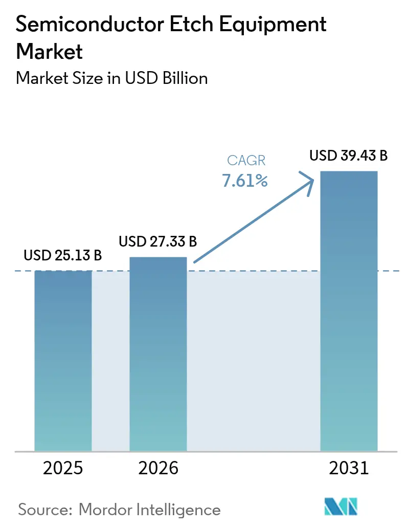
| Market Size (2026) | USD 27.33 Billion |
| Market Size (2031) | USD 39.43 Billion |
| Growth Rate (2026 - 2031) | 7.61% CAGR |
| Fastest Growing Market | North America |
| Largest Market | Asia-Pacific |
| Market Concentration | High |
Major Players.webp) *Disclaimer: Major Players sorted in no particular order Image © Mordor Intelligence. Reuse requires attribution under CC BY 4.0. | |
Semiconductor Etch Equipment Market Analysis by Mordor Intelligence
The semiconductor etch equipment market size was valued at USD 25.13 billion in 2025 and estimated to grow from USD 27.33 billion in 2026 to reach USD 39.43 billion by 2031, at a CAGR of 7.61% during the forecast period (2026-2031). Momentum reflects the multiplication of etch steps in sub-3 nanometer logic, the migration to gate-all-around transistors, the vertical scaling of 300-plus-layer NAND, and the adoption of high-bandwidth memory stacks that require through-silicon vias with aspect ratios above 100:1. Surging subsidy-backed capacity in the United States and Europe is raising order visibility for 2027-2029 installs, while Asia-Pacific continues to anchor shipments through domestic wafer-start density and mature-node localization programs. Price-performance gains in atomic layer etch systems have widened the cost gap with legacy reactive-ion platforms, accelerating tool replacement cycles. At the same time, environmental rules on fluorinated gases are compelling vendors to co-develop low-global-warming-potential chemistries, favoring incumbents that can leverage application labs and an installed base of more than 18,000 wet benches worldwide.
Key Report Takeaways
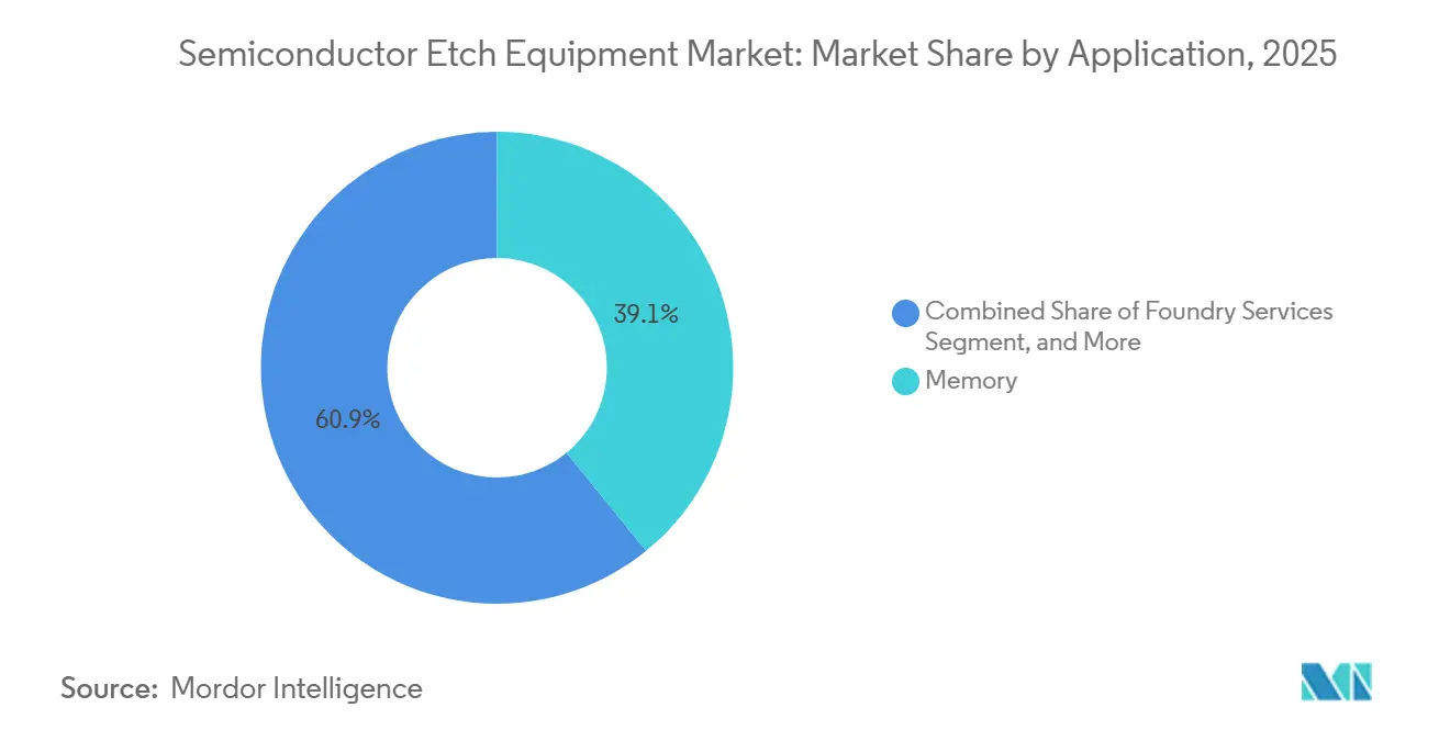
- By application, memory led with 39.12% of the semiconductor etch equipment market share in 2025, whereas advanced packaging and HBM are projected to advance at a 9.88% CAGR between 2026 and 2031.
- By equipment type, wet etch systems captured 68.89% revenue share in 2025; atomic layer etch tools represent the fastest-growing category, expanding at an 8.03% CAGR to 2031.
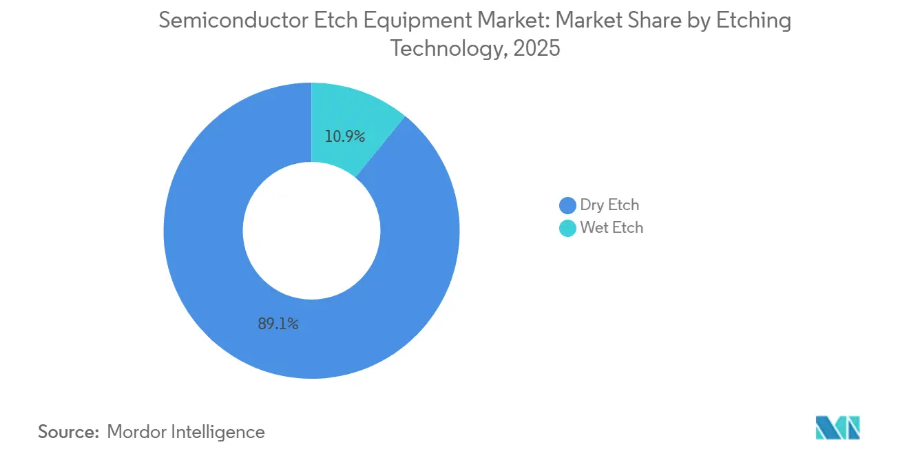
- By etching technology, wet chemistry dominated with 89.11% share during 2025, while dry plasma platforms are set to post a 7.71% CAGR owing to sub-10 nanometer feature requirements.
- By process type, front-end-of-line etching held 63.32% share in 2025; back-end-of-line and hybrid-bonding steps together are forecast to grow at an 8.01% CAGR through 2031.
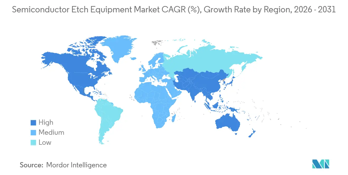
- By geography, Asia-Pacific commanded 56.52% of 2025 revenue, yet North America is expected to log the fastest regional growth at an 8.98% CAGR on the strength of CHIPS Act-funded fabs.
Note: Market size and forecast figures in this report are generated using Mordor Intelligence’s proprietary estimation framework, updated with the latest available data and insights as of 2026.
Global Semiconductor Etch Equipment Market Trends and Insights
Drivers Impact Analysis*
| Driver | (~) % Impact on CAGR Forecast | Geographic Relevance | Impact Timeline |
|---|---|---|---|
| Equipment miniaturization below 3 nm nodes | +2.1% | Global, led by Taiwan and South Korea | Medium term (2-4 years) |
| Rapid capacity-build in Chinese foundries | +1.8% | China, with spillover to Southeast Asia | Short term (≤ 2 years) |
| Transition to gate-all-around (GAA) transistors | +1.6% | Taiwan, South Korea, United States | Medium term (2-4 years) |
| U.S. and EU fab-subsidy outlays (CHIPS Acts) | +1.3% | North America and Europe | Long term (≥ 4 years) |
| On-tool AI-driven adaptive plasma chemistries | +0.9% | Global, concentrated in leading-edge fabs | Medium term (2-4 years) |
| Etch-as-a-service subscription business models | +0.7% | North America, Europe, select Asia-Pacific customers | Long term (≥ 4 years) |
| Source: Mordor Intelligence | |||


Equipment Miniaturization Below 3 nm Nodes
Increasing line-edge precision requirements have transformed etch from material removal into angstrom-level sculpting. TSMC’s N2 pilot lines tightened within-wafer uniformity to 0.8 nanometers during 2025, compelling a shift toward atomic layer etch platforms that pulse reactants and purge gases in sub-second cycles.[1]TSMC Investor Relations, “TSMC Technology Symposium 2025,” tsmc.com Samsung’s SF2 process entered volume production in 2026 with backside power delivery that relies on through-silicon vias deeper than 120 micrometers, a depth where conventional reactive-ion chambers exhibit micro-loading and sidewall bowing.[2]Samsung Foundry, “Samsung Foundry Forum 2025,” samsungfoundry.com Intel’s 18A RibbonFET nodes require selective lateral recess steps that account for 22% of yield loss if plasma parameters drift, amplifying demand for real-time endpoint control. Each incremental nanometer of scaling now adds close to USD 180 million in etch investment per 50,000-wpm fab, reinforcing consolidation among logic foundries and accelerating retirement of 200-millimeter lines. Vendors with field-upgradable chambers are therefore positioned to capture recurring revenue from recipe conversions rather than greenfield installs.
Rapid Capacity-Build in Chinese Foundries
Chinese etch shipments topped USD 4.2 billion in 2025 despite export curbs on leading-edge lithography.[3]Reuters, “Mattson Technology Introduces Microwave Plasma Etcher,” reuters.com SMIC and Hua Hong together added 85,000 wpm of 28-40 nanometer capacity, targeting automotive and IoT designs where etch selectivity for high-k dielectrics defines write-erase endurance. NAURA’s Primo nD-series platforms sell for roughly 65% of rival tools yet match process uniformity above 14 nanometers, compressing average selling prices across the semiconductor etch equipment market. Domestic utilization slipped to 72% in early 2026, below the 85% threshold for break-even returns, signaling that tool demand could plateau by 2027 unless export outlets absorb the surplus.
Transition to Gate-All-Around (GAA) Transistors
GAA multiplies etch complexity, with Samsung’s 3 nanometer flow requiring 11 discrete plasma steps to free suspended nanosheets versus six for FinFET equivalents. Intel’s hybrid three-sheet stack uses atomic layer etch to tune sheet thickness between 5 and 7 nanometers, trading off drive current against leakage. TSMC’s backside power rails introduce via aspect ratios of 100:1, forcing chamber pressure control within ±2 millitorr to suppress sidewall roughness. Lam Research’s Flex series secured 42% of GAA-related etch wins in 2025, while Applied Materials’ Sculpta ALE commanded a USD 1.8 million ASP, triple that of standard dry etchers. High tool prices but superior margins are encouraging incumbents to bundle deposition and metrology, locking in process integration fees.
U.S. and EU Fab-Subsidy Outlays (CHIPS Acts)
By end-2025, USD 18.3 billion in U.S. grants had been awarded, mostly to Intel, TSMC, Samsung, and Micron, with milestone-based disbursement tied to domestic-content ratios. Intel’s Ohio and Arizona projects alone require about USD 4.5 billion in etch tools through 2028. In Europe, EUR 10 billion of support for Intel Magdeburg drives two fabs targeting 18A nodes, though permitting and electricity prices near EUR 0.32 per kWh risk timeline slippage. Vendors booked USD 7.9 billion in CHIPS-tied etch orders during 2025, but milestone payments expose them to construction delays, prompting longer receivable cycles.
Restraints Impact Analysis*
| Restraint | (~) % Impact on CAGR Forecast | Geographic Relevance | Impact Timeline |
|---|---|---|---|
| Cyclical cap-ex swings in memory sector | -1.4% | Global, concentrated in South Korea and United States | Short term (≤ 2 years) |
| Export-control volatility in RF-generator supply | -0.9% | China, with secondary effects in Southeast Asia | Medium term (2-4 years) |
| Rising tool ASPs versus ROI hurdles | -0.8% | Global, acute in memory and mature-node segments | Medium term (2-4 years) |
| High-GWP fluorinated-gas carbon-tax exposure | -0.6% | Europe, California, with emerging impact in Asia-Pacific | Long term (≥ 4 years) |
| Source: Mordor Intelligence | |||
Cyclical Cap-Ex Swings in Memory Sector
Memory spend dropped in early 2026 as DRAM ASPs retreated 18% quarter-over-quarter, pushing Micron to trim FY-2026 capex to USD 8.1 billion and SK Hynix to defer USD 1.2 billion of tool orders. Samsung cut 2026 allocation by 12% to KRW 22 trillion (USD 16.8 billion) while channeling funds toward HBM4 ramps where etch selectivity controls thermal budget. The semiconductor etch equipment market therefore sees sequential revenue dips whenever memory inventory builds, compelling vendors to offer extended payment terms and service-bundled upgrades to protect margins.
Export-Control Volatility in RF-Generator Supply
October 2025 Entity-List additions require individual licenses for RF generators above 27 MHz and 3 kW, leading Advanced Energy and MKS Instruments to cancel USD 420 million in Chinese orders. Piotech and Naura ramped domestic generator output to 12,000 units in 2025, yet current versions max out at 2.1 kW and 13.56 MHz, forcing Chinese fabs to extend etch times by 18-25%. Global OEMs have doubled inventory buffers to 90 days, tying up USD 280 million in working capital and inflating cost of goods sold. Supply bifurcation raises process-efficiency disparity between leading-edge fabs and mature-node foundries dependent on localized subsystems.
*Our forecasts treat driver/restraint impacts as directional, not additive. The impact forecasts reflect baseline growth, mix effects, and variable interactions.
Segment Analysis
By Application: Memory Leads, Packaging Accelerates
Memory held 39.12% revenue share in 2025, sustaining the largest slice of the semiconductor etch equipment market size, yet advanced packaging is poised to climb at a 9.88% CAGR through 2031. DRAM capacitor trenches and 300-layer NAND stacks require high-aspect-ratio etch, whereas HBM-enabled chiplet designs introduce additional through-silicon via steps. Packaging demand is amplified by artificial-intelligence accelerators that integrate eight or more HBM3E stacks, each stack adding three dedicated etch steps for micro-bump reveal and wafer thinning. Tool specifications now emphasize ultra-low sidewall roughness and precise depth control to avoid via tilt, creating upgrade pull across existing 300-millimeter lines.
Logic and MPU applications contributed roughly 28% of 2025 revenue as Intel’s 18A and TSMC’s N2 pilots reached risk-production, while foundry services accounted for about 18%. Power and discrete devices represented 7%, driven by electric-vehicle inverters that rely on trench etch in silicon-carbide wafers. MEMS, sensors, and optoelectronic devices split the remainder. Over the forecast horizon, the semiconductor etch equipment market share gap between memory and advanced packaging narrows because hybrid bonding multiplies BEOL steps faster than DRAM or NAND capacity grows, offering vendors fresh annuity streams via chamber upgrade kits.


By Equipment Type: Wet Systems Dominate, ALE Gains Pace
Wet benches processed 68.89% of etch-related wafer volume in 2025 thanks to batch economics of USD 0.12 per wafer, underlining their entrenched position in the semiconductor etch equipment market. Atomic layer etch platforms, however, are forecast to post an 8.03% CAGR to 2031 as sub-3 nanometer gates and 300-layer NAND require angstrom-level selectivity. Inductively coupled plasma etchers covered 12% of 2025 spend, favored for metal-line patterning where high ion density yields vertical profiles. Reactive-ion systems held 9% but face retirement as 200-millimeter fabs age, whereas deep reactive-ion tools supported MEMS and power devices with 6% share. Vendors now bundle AI-driven plasma control that automatically tunes process windows, shaving qualification cycles by 20% and reducing wafer scrap.
Capex decisions in 2026 show a dual-track path: foundries order ALE tools for leading nodes, while automotive and industrial customers refresh wet benches for 200-millimeter capacity, extending their depreciation horizon beyond 2030. This divergence lowers blended ASPs but raises service-mix contribution as vendors retrofit legacy chambers with endpoint metrology.
By Etching Technology: Wet Entrenched, Dry Expands
Wet chemistries retained 89.11% revenue share in 2025, reflecting their ubiquity in photoresist strip and surface cleans. Dry etch is predicted to grow 7.71% annually through 2031, lifting its proportion of the semiconductor etch equipment market size as plasma processes become indispensable for anisotropic profiles. Environmental levies on perfluorocarbon gases added about 8% to dry-etch consumable costs in 2025, yet tool upgrades that cut gas flow by 30% have nearly neutralized this penalty. Hybrid wet-dry flows are emerging: Lam Research and TSMC patented a sequence that pairs dilute hydrofluoric clean with pulsed-bias plasma, reducing residue by 45% while cutting water use by 30%.
For 3 nanometer GAA and 18A RibbonFET, chipmakers allocate roughly equal counts of wet and dry steps, but dry platforms account for 70% of etch-equipment value because of higher ASPs and chamber-per-process requirements. Consequently, the semiconductor etch equipment market is shifting toward single-wafer, high-throughput dry tools equipped with in-situ metrology, a transition that underpins future service revenue through software subscriptions and recipe analytics.
By Process Type: FEOL Dominates, BEOL Gains Momentum
Front-end-of-line processes—including gate recess, source-drain, and shallow trench isolation—generated 63.32% of 2025 demand and remain the primary contributor to the semiconductor etch equipment market share. Yet back-end-of-line steps are forecast to deliver an 8.01% CAGR as copper-damascene stacks proliferate and hybrid bonding integrates logic and memory dies inside single packages. Intel’s 18A adds three extra BEOL metal layers relative to Intel 7, increasing via count by 28% and driving procurement of conductor-etch chambers with 20:1 selectivity between copper and low-k dielectrics. Through-silicon and backside vias in advanced packaging further blur the line between BEOL and wafer-level assembly, expanding addressable market for vendors that traditionally served only FEOL.
SPTS and Veeco together seized 22% of redistribution-layer etch orders in 2025, proving that niche players can carve share when incumbents lack dedicated packaging portfolios. Over the outlook period, FEOL revenue remains larger, but BEOL’s faster growth shifts profit pools toward suppliers with conductor-etch expertise and robust copper corrosion mitigation.
Geography Analysis
Asia-Pacific generated 56.52% of 2025 sales, anchored by Taiwan’s foundry cluster, South Korea’s memory lines, and China’s localization drive. TSMC alone absorbed an estimated USD 6.8 billion of etch hardware for N3 volume ramps and N2 pilots, while Samsung booked USD 3.2 billion supporting 3 nanometer GAA and 1-beta DRAM. Japanese spend was largely Kioxia’s 3D NAND expansion and Renesas automotive MCU conversions, whereas India and Southeast Asia combined for under 2% as greenfield fabs awaited policy clarity.
North America is projected to lead regional growth at 8.98% CAGR through 2031 because CHIPS Act grants advance multiple mega-fab projects. Intel’s Ohio and Arizona campuses, TSMC’s Phoenix site, and Micron’s New York DRAM fab together require roughly USD 12 billion in etch tools between 2026 and 2029. The semiconductor etch equipment market size attributable to North America could therefore double its 2025 baseline by the end of the decade. However, milestone-based funding and union-labor negotiations introduce schedule risk that vendors must hedge through flexible shipment windows and progress-linked invoicing.
Europe captured 12% of 2025 revenue, driven by Intel Magdeburg and STMicroelectronics Crolles. Yet rising energy costs—average industrial electricity at EUR 0.32 per kWh, triple U.S. rates—threaten project IRRs, prompting lobbying for renewable-energy subsidies. The Middle East, Africa, and South America remained below 3% combined, although Saudi Arabia’s NEOM initiative and Brazil’s auto-chip incentives may unlock niche demand post-2027.

Competitive Landscape
Applied Materials, Lam Research, and Tokyo Electron controlled about 75% of global revenue in 2025, characterizing the semiconductor etch equipment market as highly concentrated. Applied Materials led at 32% owing to strength in dielectric and atomic layer etch, while Lam Research followed at 28% through conductor-etch and packaging platforms. Tokyo Electron held roughly 15% with its Tactras line featuring in-situ metrology. Chinese challengers NAURA and AMEC doubled domestic share to 18% between 2023 and 2025 but remain limited to ≥14 nanometer nodes because of RF-generator license barriers.
Competitive strategy is migrating from tool sales to platform ecosystems. Applied’s Integrated Materials Solutions bundle deposition, etch, and metrology inside a common transfer module, generating 42% of its etch revenue in 2025. Lam Research now derives 34% of revenue from spares, upgrades, and software analytics that cut particle excursions by 40%. Tokyo Electron collaborates with TSMC on cryogenic etch for backside power delivery networks, targeting electromigration reduction. Emerging disruptors include Mattson Technology’s microwave-plasma etcher, eliminating RF generators and lowering energy use by 35%. Oxford Instruments, Plasma-Therm, and SAMCO focus on silicon-carbide and GaN power devices, markets expected to grow double digits through 2031. The competitive trajectory implies a bifurcation: incumbents retain leading-edge dominance, while regional specialists carve mature-node and power-device niches.
Semiconductor Etch Equipment Industry Leaders
Applied Materials, Inc.
Lam Research Corp.
Tokyo Electron Ltd.
Hitachi High-Tech Corp.
Plasma-Therm LLC
- *Disclaimer: Major Players sorted in no particular order

Recent Industry Developments
- February 2026: Applied Materials unveiled the Sculpta Pro ALE system with dual-chamber architecture that lifts throughput 35% to 80 wph for gate-all-around nodes.
- January 2026: Lam Research expanded its Tualatin, Oregon, factory by 120,000 sq ft to boost Flex-series output 25%, preparing for CHIPS Act demand.
- December 2025: Tokyo Electron and TSMC co-developed a cryogenic etch platform targeting 2 nanometer backside power rails.
- November 2025: NAURA won a USD 380 million order from CXMT for 45 Primo nD dry etchers, China’s largest single contract.


Global Semiconductor Etch Equipment Market Report Scope
Semiconductor etch equipment is a device used to remove selective materials from the surface of the silicon wafer substrate by using various chemicals. The etching process removes the material from the surface of the semiconductor to create patterns according to its applications. It is being used in the semiconductor device fabrication process.
The Semiconductor Etch Equipment Market Report is Segmented by Application (Logic/MPU, Memory, Foundry Services, Power and Discrete Devices, MEMS and Sensors, Advanced Packaging/HBM, Others), Equipment Type (RIE, ICP Etcher, DRIE, ALE, Wet Etch Systems, HARP), Etching Technology (Dry Etch, Wet Etch), Process Type (FEOL, BEOL, Advanced-Packaging Etching), and Geography (North America, South America, Europe, Asia-Pacific, Middle East, Africa). Market Forecasts are Provided in Value (USD).
By Application
| Logic / MPU |
| Memory |
| Foundry Services |
| Power and Discrete Devices |
| MEMS and Sensors |
| Advanced Packaging / HBM |
| Others |
By Equipment Type
| Reactive Ion Etcher (RIE) |
| Inductively Coupled Plasma (ICP) Etcher |
| Deep RIE (DRIE) |
| Atomic Layer Etch (ALE) |
| Wet Etch Systems |
| High-Aspect-Ratio Etch (HARP) |
By Etching Technology
| Dry Etch |
| Wet Etch |
By Process Type
| Front-End-of-Line (FEOL) Etching |
| Back-End-of-Line (BEOL) Etching |
| Advanced-Packaging Etching |
By Geography
| North America | United States |
| Canada | |
| Mexico | |
| South America | Brazil |
| Argentina | |
| Rest of South America | |
| Europe | Germany |
| United Kingdom | |
| France | |
| Italy | |
| Spain | |
| Rest of Europe | |
| Asia-Pacific | China |
| India | |
| Japan | |
| South Korea | |
| Australia and New Zealand | |
| Rest of Asia-Pacific | |
| Middle East | Saudi Arabia |
| United Arab Emirates | |
| Turkey | |
| Rest of Middle East | |
| Africa | South Africa |
| Nigeria | |
| Egypt | |
| Rest of Africa |
| By Application | Logic / MPU | |
| Memory | ||
| Foundry Services | ||
| Power and Discrete Devices | ||
| MEMS and Sensors | ||
| Advanced Packaging / HBM | ||
| Others | ||
| By Equipment Type | Reactive Ion Etcher (RIE) | |
| Inductively Coupled Plasma (ICP) Etcher | ||
| Deep RIE (DRIE) | ||
| Atomic Layer Etch (ALE) | ||
| Wet Etch Systems | ||
| High-Aspect-Ratio Etch (HARP) | ||
| By Etching Technology | Dry Etch | |
| Wet Etch | ||
| By Process Type | Front-End-of-Line (FEOL) Etching | |
| Back-End-of-Line (BEOL) Etching | ||
| Advanced-Packaging Etching | ||
| By Geography | North America | United States |
| Canada | ||
| Mexico | ||
| South America | Brazil | |
| Argentina | ||
| Rest of South America | ||
| Europe | Germany | |
| United Kingdom | ||
| France | ||
| Italy | ||
| Spain | ||
| Rest of Europe | ||
| Asia-Pacific | China | |
| India | ||
| Japan | ||
| South Korea | ||
| Australia and New Zealand | ||
| Rest of Asia-Pacific | ||
| Middle East | Saudi Arabia | |
| United Arab Emirates | ||
| Turkey | ||
| Rest of Middle East | ||
| Africa | South Africa | |
| Nigeria | ||
| Egypt | ||
| Rest of Africa | ||


Key Questions Answered in the Report
How large is the semiconductor etch equipment market today?
The semiconductor etch equipment market size stood at USD 27.33 billion in 2026 and is on track to reach USD 39.43 billion by 2031.
What CAGR is forecast for etch equipment between 2026 and 2031?
Industry revenue is projected to advance at a 7.61% CAGR over the 2026-2031 period.
Which segment is expanding fastest?
Advanced packaging and high-bandwidth memory etch steps are forecast to grow at a 9.88% CAGR through 2031, outpacing all other application areas.
Who are the leading vendors?
Applied Materials, Lam Research, and Tokyo Electron collectively controlled roughly 75% of global revenue in 2025.
What region will post the strongest growth?
North America is expected to register the fastest regional CAGR at 8.98%, buoyed by CHIPS Act-funded mega-fab construction.
How will environmental rules affect tool demand?
EU carbon levies on fluorinated gases are increasing dry-etch consumable costs, prompting co-development of low-GWP chemistries and raising demand for upgraded plasma chambers.
Page last updated on:


