
Magneto-resistive RAM (MRAM) Market Size and Share
Market Overview
| Study Period | 2020 - 2031 |
|---|---|
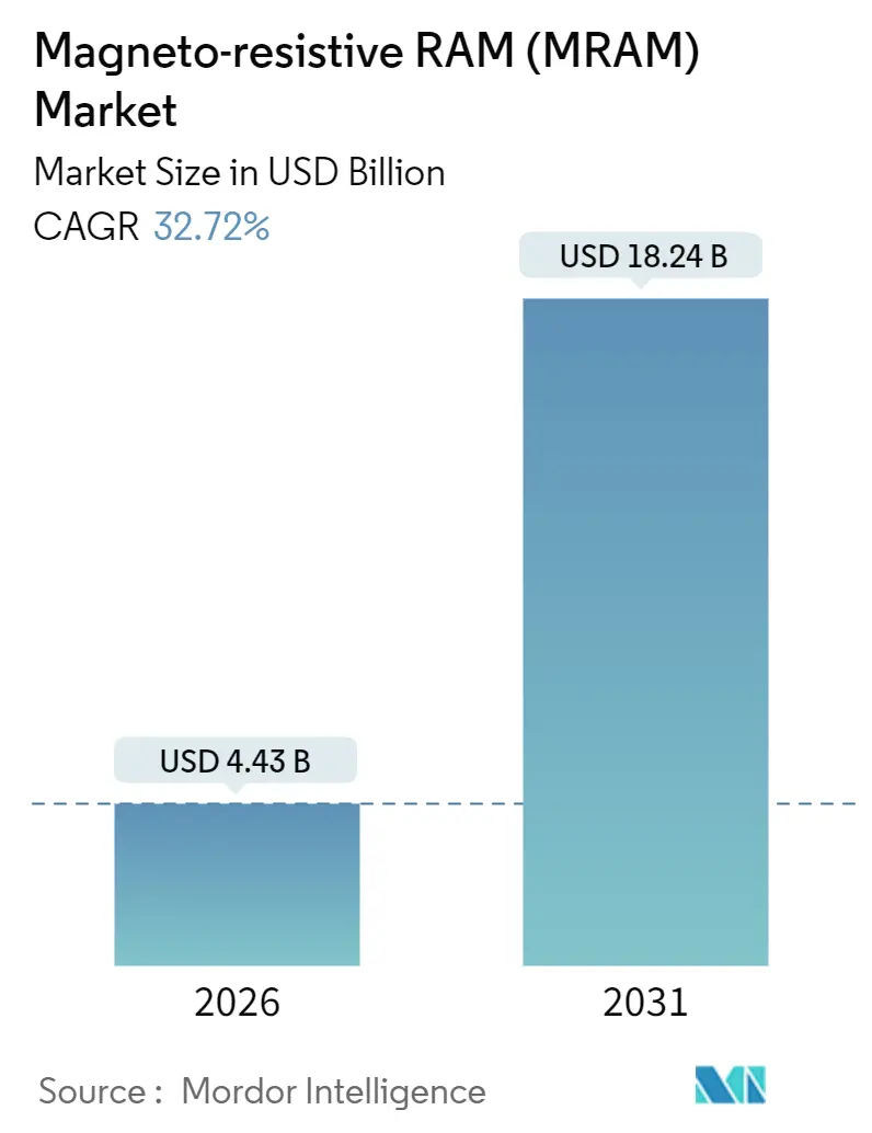
| Market Size (2026) | USD 4.43 Billion |
| Market Size (2031) | USD 18.24 Billion |
| Growth Rate (2026 - 2031) | 32.72 % |
| Fastest Growing Market | Middle East |
| Largest Market | Asia Pacific |
| Market Concentration | Medium |
Major Players *Disclaimer: Major Players sorted in no particular order Image © Mordor Intelligence. Reuse requires attribution under CC BY 4.0. | |
Magneto-resistive RAM (MRAM) Market Analysis by Mordor Intelligence
The Magneto-resistive RAM (MRAM) market size stands at USD 4.43 billion in 2026 and is projected to reach USD 18.24 billion by 2031, expanding at a 32.72% CAGR over the forecast period. Robust functional-safety mandates in automotive electronics, rapid deployment of battery-constrained IoT edge nodes, and the rise of on-device AI inference that benefits from compute-in-memory architectures are the primary growth engines. Foundries in Asia-Pacific have qualified 22 nm and 28 nm embedded processes that bundle MRAM cells with logic, cutting component count and enabling instant-on operation in mission-critical controllers. In parallel, research labs across Europe and North America are commercializing voltage-controlled switching mechanisms that halve write energy and push endurance past 10¹⁵ cycles. Competitive intensity is therefore shifting from pure hardware sales toward IP licensing and design services that monetize process know-how, controller firmware, and endurance-focused error-correction schemes.
Key Report Takeaways
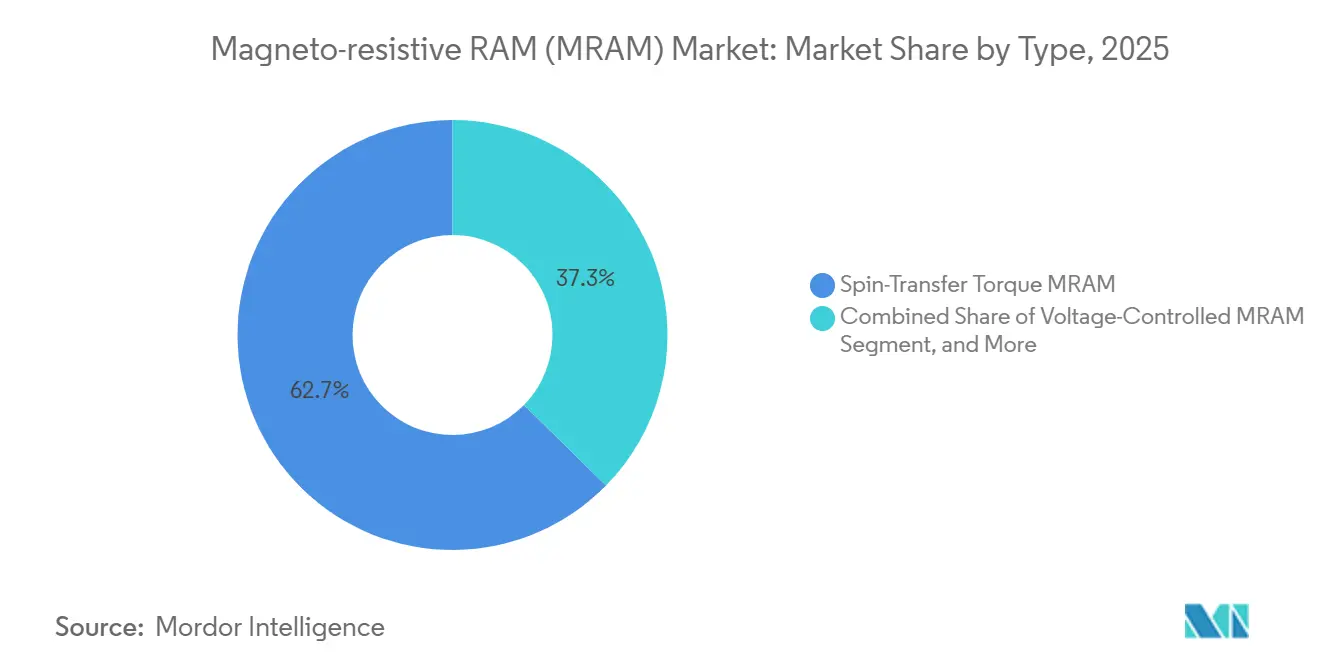
- By type, spin-transfer torque captured 62.66% of Magneto-resistive RAM (MRAM) market share in 2025. Voltage-controlled MRAM is forecast to expand at a 33.21% CAGR through 2031.
- By offering, embedded devices held 62.00% of MRAM market share in 2025. IP cores and design services are projected to grow at a 33.83% CAGR to 2031.
- By technology node, processes at or below 28 nm accounted for 46.00% of the MRAM market size in 2025 and are poised for a 34.02% CAGR through 2031.
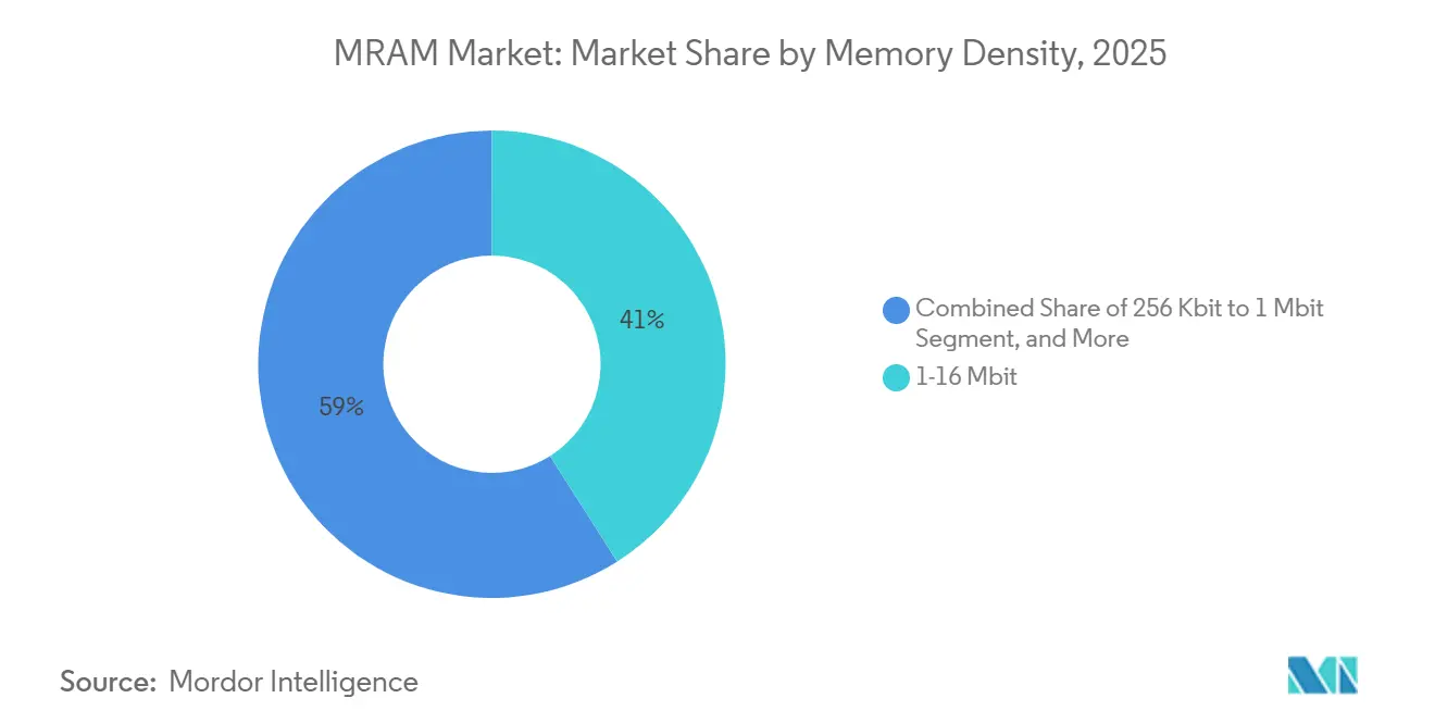
- By memory density, the 1-16 Mbit range accounted for 41% of the MRAM market size in 2025 and sub-256 Kbit devices are expected to advance at a 34.21% CAGR through 2031.
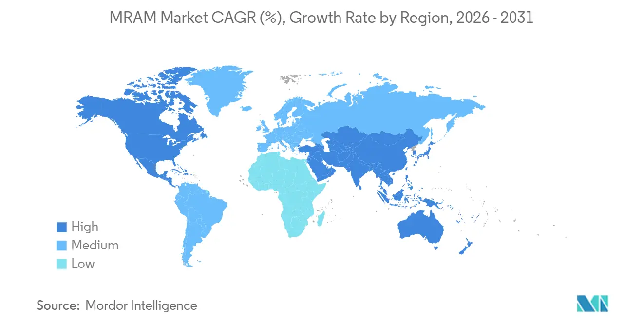
- By geography, Asia-Pacific generated 48.00% of 2025 revenue, while the Middle East is expected to advance at a 34.52% CAGR between 2026-2031.
Note: Market size and forecast figures in this report are generated using Mordor Intelligence’s proprietary estimation framework, updated with the latest available data and insights as of January 2026.
Global Magneto-resistive RAM (MRAM) Market Trends and Insights
Drivers Impact Analysis*
| Driver | (~) % Impact on CAGR Forecast | Geographic Relevance | Impact Timeline |
|---|---|---|---|
| Proliferation of IoT and Edge Devices | +6.50% | Global, with APAC and North America leading deployments | Medium term (2-4 years) |
| Rising Adoption in Automotive Functional-Safety Systems | +5.80% | APAC (Japan, South Korea, China), Europe (Germany), North America | Long term (≥ 4 years) |
| Increasing Miniaturization in Consumer Electronics | +3.20% | APAC (China, South Korea, Taiwan), North America | Short term (≤ 2 years) |
| Deployment as Storage Class Memory in Data Centers | +4.10% | North America, Europe, APAC (Singapore, Hong Kong) | Medium term (2-4 years) |
| Defense-Grade Radiation Hardness for Satellite Edge Computing | +2.90% | North America, Europe, Middle East (Israel), APAC (Japan) | Long term (≥ 4 years) |
| On-Chip NVM Scratchpads for AI Accelerators | +3.80% | Global, with North America and APAC leading AI chip development | Medium term (2-4 years) |
| Source: Mordor Intelligence | |||


Proliferation Of IoT and Edge Devices
Industrial automation, smart metering, and wearable health monitors now embed local processing to cut latency and protect data privacy. Octal-interface Magneto-resistive RAM (MRAM) parts deliver 400 MB/s throughput, replacing battery-backed SRAM and eliminating supercapacitors. Microcontroller makers cite 90% lower standby power versus flash, enabling five-year battery life for condition-monitoring sensors. High endurance means designers no longer provision wear-levelling firmware, saving precious ROM space. As component footprints shrink, more edge boards adopt MRAM arrays that share the supply rail with logic blocks, removing board-level voltage translators and trimming bill-of-materials cost.[1]Everspin Technologies, “PERSYST xSPI STT-MRAM,” everspin.com
Rising Adoption in Automotive Functional-Safety Systems
Powertrain and ADAS controllers must retain calibration data across ignition cycles without latency or wear-levelling overhead. Embedded MRAM in 16 nm FinFET microcontrollers supports ISO 26262 ASIL-D safety targets while operating from -40 °C to +125 °C. Unlimited write endurance avoids field failures that could trigger costly recalls. Electric-vehicle battery-management units write state-of-charge logs thousands of times per second, a duty cycle traditional flash cannot sustain. With automotive semiconductors moving to 22 nm and below, MRAM cells scale in lockstep, delivering multi-megabit densities within tightly constrained die areas.[2]NXP Semiconductors, “S32K5 MCU Introduction,” nxp.com
Miniaturization In Consumer Electronics
Smartphones, wearables, and AR headsets demand low-leakage memory to extend battery life while keeping firmware instantly accessible after deep sleep. Embedded Magneto-resistive RAM (MRAM) in 14 nm application processors eliminates the need for separate NOR flash dies, freeing board space for larger batteries or additional sensors. Sub-10 µs wake-to-active times enhance user experience in voice-activated earbuds and health trackers. Component consolidation reduces overall device mass, supporting lighter form factors that appeal to style-conscious consumers.
On-Chip NVM Scratchpads For AI Accelerators
Edge inference engines store model weights in MRAM, allowing compute-in-memory operations that cut data movement energy by an order of magnitude. Prototype analog chips show 10× lower power than SRAM-based designs and sustain inference after power loss, critical for autonomous drones and industrial robots that must restart safely. Engineering services deals indicate commercial traction, with MRAM vendors tailoring controller IP for convolutional neural networks and transformer blocks. As model parameters balloon, embedded MRAM arrays at 16 nm and below deliver hundreds of megabits without incurring standby leakage penalties seen in eDRAM.
Restraints Impact Analysis*
| Restraint | (~) % Impact on CAGR Forecast | Geographic Relevance | Impact Timeline |
|---|---|---|---|
| High Fabrication Cost of Perpendicular MTJ Process | -2.40% | Global, with higher impact in regions lacking advanced foundry infrastructure | Medium term (2-4 years) |
| Competition from Alternative NVM Technologies | -2.10% | Global, with APAC and North America leading ReRAM and PCM development | Short term (≤ 2 years) |
| Yield Variability at Sub-28 nm Nodes | -1.80% | APAC (Taiwan, South Korea), North America | Medium term (2-4 years) |
| Tooling Supply-Chain Bottlenecks | -1.30% | Global, with dependencies on ion-beam etching and deposition equipment vendors | Short term (≤ 2 years) |
| Source: Mordor Intelligence | |||
High Fabrication Cost Of Perpendicular MTJ Process
Perpendicular magnetic tunnel junction stacks add up to 40 back-end-of-line steps, including ion-beam milling and ultra-high-vacuum MgO deposition. Tool sets cost millions of U.S. dollars and demand sub-angstrom surface control, pushing wafer-level costs to roughly twice that of embedded flash at comparable nodes. Only a handful of foundries have qualified these modules, limiting supply and keeping average selling prices elevated. Until equipment suppliers widen availability and second-source capacity emerges, OEMs remain cautious about single-sourcing critical memory.
Competition From Alternative NVM Technologies
Resistive RAM and phase-change memory promise lower bit cost and similar endurance, especially in microcontrollers that do not require the radiation hardness MRAM offers. A leading foundry plans high-volume ReRAM production on its 22FDX+ line beginning 2026, creating price pressure for embedded non-volatile options. Benchmark papers report sub-10 ns write speeds and 10⁹-cycle durability for phase-change cells, narrowing the performance gap. Should these technologies achieve parity on retention and endurance, Magneto-resistive RAM (MRAM) vendors may need to pivot toward aerospace, defense, and AI compute niches where deterministic latency and radiation immunity remain differentiators.
*Our forecasts treat driver/restraint impacts as directional, not additive. The impact forecasts reflect baseline growth, mix effects, and variable interactions.
Segment Analysis
By Type: STT-MRAM Dominates, VC-MRAM Accelerates
Spin-transfer torque devices captured 62.66% Magneto-resistive RAM (MRAM) market share in 2025 on the strength of qualified 22 nm and 28 nm flows that meet automotive and industrial reliability standards. Toggle MRAM persists in extreme-temperature systems, such as oil-field sensors, because its in-plane geometry tolerates 200 °C excursions. Voltage-controlled switching reduces write current by roughly 50%, a critical win for edge AI accelerators, and is forecast to clock a 33.21% CAGR through 2031. Spin-orbit torque remains in the research domain, but its decoupled read-write paths suggest write endurance exceeding 10¹⁵ cycles, positioning it as a long-term successor.
Adoption momentum proves two-tiered. Mainstream controllers favour mature STT-MRAM for near-term programs, whereas AI startups engage with research fabs to prototype voltage-controlled arrays that slash energy per inference. Industry roadmaps show pilot VC-MRAM lines at 14 nm by 2028. If yield ramps on schedule, the MRAM market could migrate to this topology for high-volume consumer processors, reinforcing the technology’s twice-per-decade architecture refresh cadence.


By Offering: Embedded Leads, IP Licensing Surges
Embedded variants accounted for 62.00% share of Magneto-resistive RAM (MRAM) market in 2025 because they integrate directly into logic wafers, eliminating external packages and boosting system reliability. Stand-alone serial parts still serve industrial retrofit boards that need a pin-compatible replacement for parallel SRAM. The MRAM market size for IP cores and design services, however, is projected to expand at a 33.83% CAGR, reflecting fabless demand to license hardened memory macros without owning masks. Controller IP firms bundle error-correction engines that mitigate bit-error-rate drift at sub-28 nm, easing qualification for automotive ASIL-D targets.
As more OEMs embrace chiplets and heterogeneous integration, MRAM macro IP can be dropped into a reticle on advanced interposers, shortening design cycles. Vendors thus pivot from component revenue toward annuity-style royalties, mirroring the shift ARM catalysed in CPU cores. This structural change underpins healthier gross margins despite falling per-bit prices in commodity densities.
By Technology Node: Sub-28 nm Scales, Legacy Nodes Persist
Nodes at or below 28 nm generated 46.00% of the Magneto-resistive RAM (MRAM) market size in 2025 and are trending toward a 34.02% CAGR because leading-edge automotive and AI chips crave higher density. A 16 nm FinFET microcontroller now packs over 8 MB of non-volatile code storage within the same die footprint that held 2 MB on 40 nm, proving the density advantage. Yet legacy 55 nm and 40 nm flows remain indispensable for radiation-hardened satellites and extreme-temperature industrial drives where larger geometries improve robustness.
Foundries monetize both ends of the spectrum. Premium wafers on EUV nodes target consumer flagships, while fully depreciated 65 nm lines capture long-tail industrial programs with 15-year lifecycles. The bifurcation supports stable overall wafer demand, cushioning the MRAM market from cyclic swings in any single end-use sector.
By Memory Density: 1-16 Mbit Anchors, Sub-256 Kbit Accelerates
Densities between 1 Mbit and 16 Mbit held 41.00% share in 2025 of Magneto-resistive RAM (MRAM) market, favoured by automotive control units and programmable logic controllers that log calibration data. Below 256 Kbit, growth is fastest, topping a 34.21% CAGR, because smart tags, tire-pressure sensors, and disposable medical patches need just kilobytes of firmware but must eliminate standby leakage. At the other extreme, 128 Mbit serial devices now buffer enterprise SSD writes, while gigabit-class die target data-center metadata logging and satellite edge compute platforms.
The segmentation confirms a barbell demand profile. Ultralow-density parts proliferate in billions of sensor nodes, while high-density parts capture margin-rich storage and aerospace sockets. Mid-density components remain the workhorse that sustains foundry utilization rates.
By Application: Automotive Leads, IoT Surges
Automotive electronics contributed 29.00% of 2025 revenue, anchored by stability control and battery-management modules. Design wins at multiple tier-one suppliers underpin steady volumes through the decade because platform lifetimes exceed seven years. IoT and edge computing devices, however, should post a 33.57% CAGR, outpacing all other segments. Smart meters now ship with MRAM to preserve cumulative usage registers even if installers cut power abruptly. Wearable ECG patches leverage MRAM’s instant capture of high-frequency data bursts without risking corruption on battery depletion.
Enterprise storage, healthcare instrumentation, industrial robots, and smart-card authentication together form a balanced second tier of demand. Each niche values MRAM’s unique mix of endurance, shock tolerance, and power-fail safety, insulating the Magneto-resistive RAM (MRAM) market from reliance on any single vertical.
Geography Analysis
MRAM Market in North America
Asia-Pacific generated 48.00% of Magneto-resistive RAM (MRAM) market revenue in 2025, reflecting deep foundry capacity in Taiwan and South Korea and surging automotive semiconductor demand in China. Government incentives, such as South Korea’s USD 27 million program that funds 48 memory projects, accelerate process tweaks and mask re-spins. Japan’s collaboration between a leading university and a regional foundry brings pilot production of voltage-controlled MRAM on-shore, reinforcing supply-chain resilience amid geopolitical uncertainty.
The Middle East is projected to post the highest regional CAGR at 34.52% between 2026-2031. Israel’s vibrant fabless cluster anchors design talent, while Gulf nations channel sovereign funds into semiconductor parks that court memory startups. Defense-grade requirements for satellite constellations dovetail with MRAM’s radiation tolerance, creating sticky demand even as cost curves improve.
North America remains pivotal for aerospace and data-center deployments. Arizona-based manufacturers logged double-digit revenue growth in 2025 from space-qualified parts, and the United States federal programs subsidize low-Earth-orbit component testing. Europe leverages its automotive supply chain in Germany and advanced R&D hubs in Belgium to pilot perpendicular MTJ stacks below 20 nm. Both regions jointly ensure that global sourcing of MRAM devices spans at least three continents, mitigating single region supply shocks.[3]South Korea Ministry of Trade, Industry and Energy, “Memory R&D Funding Announcement,” motie.go.kr

Regulatory Landscape
MRAM supply and commercialization are shaped by export controls and trade enforcement tied to semiconductors. In the United States, the Department of Commerce, Bureau of Industry and Security (BIS) expanded and clarified export-control treatment for advanced semiconductor items through actions spanning September 2024 controls (including new Commerce Control List classifications) and additional guidance in May 2026 on how licensing requirements apply based on ultimate parent and Country Group status. This raises compliance burden for cross-border MRAM shipments integrated into advanced computing systems.
Trade and industrial policy also affects risk and localization decisions. In January 2026, a Section 337 complaint involving certain MRAM devices was filed at the U.S. International Trade Commission, creating potential import-disruption exposure for suppliers and OEMs relying on U.S. inbound flows. In Europe, the EU Chips Act (Regulation 2023/1781) continues to push semiconductor ecosystem strengthening and common approaches around trusted and secure chips, which can influence qualification, documentation, and sourcing requirements for memory components used in automotive, industrial, and defense electronics.
Value Chain Analysis
MRAM value creation begins with materials and front-end process modules for magnetic tunnel junction (MTJ) stacks, including specialized cobalt-iron-boron alloys and high-purity magnesium oxide inputs, alongside critical thin-film deposition and etch toolsets used to build perpendicular MTJ layers. Equipment availability and process know-how, including sputtering, milling, and deposition control, remain gating factors. High back-end-of-line step counts and multi-year automotive and industrial qualification cycles also reinforce barriers to entry and concentrate supply among qualified fabs.
Manufacturing and commercialization span two primary routes: embedded MRAM integrated into logic processes at advanced nodes, and stand-alone or module-level products for industrial, storage, and aerospace applications distributed through OEM and channel partners. Recent supply-chain actions illustrate diversification of manufacturing footprints, including Everspin entering an initial 10-year manufacturing agreement with Microchip Technology to establish a copy-exact MRAM production line at Microchip's Fab 4 in Gresham, Oregon. At the same time, Samsung's disclosure of embedded MRAM implementation and mass-production yield at an 8 nm FinFET process points to progress on high-volume embedded integration. Downstream, MRAM adoption is accelerated by controller and firmware IP, error-correction schemes, and system integration work that helps customers meet reliability targets such as AEC-Q100 for automotive-grade deployments.
Competitive Landscape
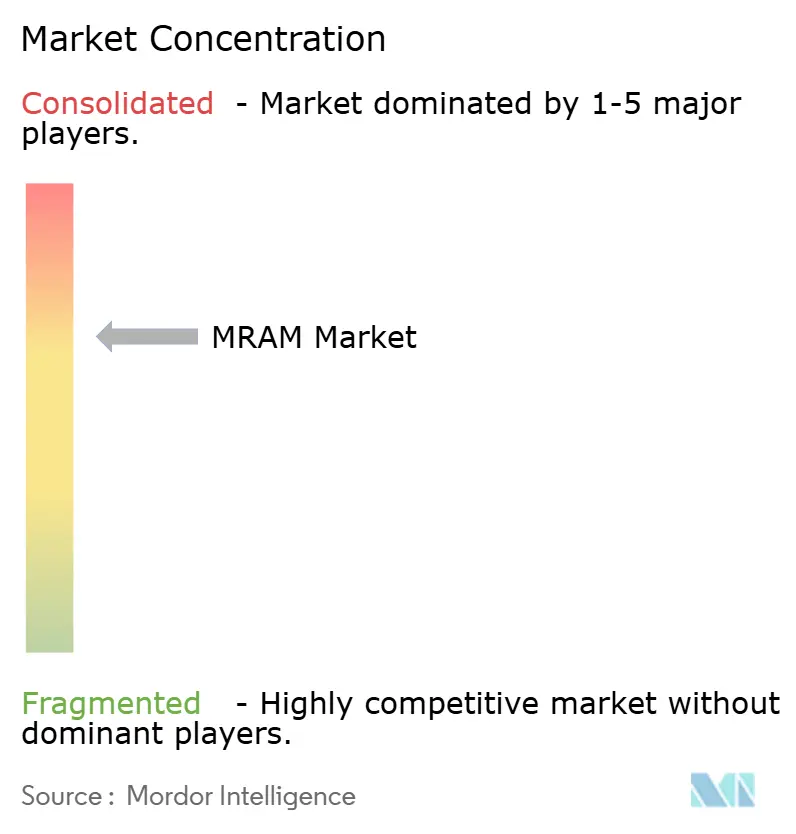
The five largest suppliers command roughly 45% of MRAM market share, indicating moderate concentration. Two pure-play vendors focus on discrete and IP business models, while three global foundries embed MRAM in mainstream logic processes. Strategic moves in 2025 included an engineering-services contract worth USD 4.1 million to adapt compute-in-memory architectures and a 22FDX+ ReRAM announcement that intensifies cross-technology competition. Leading OEMs cite endurance and deterministic latency as reasons to dual-source MRAM despite ReRAM’s cost advantage.
Integrated device manufacturers exploit scale to push qualified nodes from 28 nm to 16 nm. Meanwhile, startups secure venture rounds by specializing in voltage-controlled or spin-orbit torque physics that promise radical energy savings. Patent filings on spintronic stack engineering rose sharply in 2025, signalling that differentiation now pivots on process IP rather than basic cell structures.
Future battlegrounds include AI edge accelerators, where unified MRAM scratchpads can collapse SRAM and DRAM hierarchies, and radiation-hardened defense electronics, where incumbent MRAM suppliers already possess heritage qualification data.
Magneto-resistive RAM (MRAM) Industry Leaders
Honeywell International Inc.
Infineon Technologies AG
Intel Corporation
Avalanche Technology Inc.
Samsung Electronics Co. Ltd
- *Disclaimer: Major Players sorted in no particular order

Market Opportunities and Future Outlook
Embedded MRAM replacement of embedded flash at advanced nodes remains a central whitespace, supported by foundry and ecosystem movement toward smaller geometries where eFlash scaling is more complex. Technical disclosures at ISSCC 2026, including a 16 nm embedded STT-MRAM macro at 168 Mb with high read throughput aimed at automotive and edge AI use cases, support productization pathways for higher-density embedded non-volatile memory in controllers and accelerators that benefit from instant-on behavior and endurance.
Discrete and ruggedized MRAM opportunities are broadening where deterministic behavior and qualification are decisive, particularly across aerospace, defense, and high-reliability industrial systems. In April 2026, Everspin executed a USD 40 million agreement with a U.S. prime contractor centered on Toggle MRAM technology for defense industrial base customers, while also deepening supply resilience via a long-term manufacturing agreement with Microchip for on-shore capacity. On the interface and product side, Everspin introduced UNISYST unified-memory MRAM with xSPI connectivity and advanced its high-reliability xSPI portfolio with AEC-Q100 Grade 1 production qualification, alongside a roadmap to higher densities. This supports design-in headroom in edge nodes that want faster non-volatile storage without battery-backed SRAM or supercapacitors.
Recent Industry Developments
- April 2026: Everspin executed a USD 40 million agreement with a U.S. prime contractor to provide Toggle MRAM technology for U.S. defense industrial base customers. The deal strengthens MRAM pull-through in mission-critical programs where endurance and deterministic retention matter more than bit cost, and it supports longer production visibility for qualified parts.
- November 2025: NXP led a USD 17.5 million Series A round in Israel-based RAAAM Memory focused on spin-orbit torque MRAM development. The investment signals continued industry attention on next-generation switching mechanisms that can raise endurance and lower energy, and it broadens the MRAM innovation pipeline beyond incumbent STT and toggle designs.
- October 2024: Avalanche Technology shipped its first high-density PEMS-qualified MRAM products to the aerospace and defense sector. Shipping qualified devices advances MRAM penetration in rad-hard and space-grade applications where heritage qualification and supply assurance drive socket wins.


Research Methodology Framework and Report Scope
Market Definition and Coverage
This market covers revenues generated from magneto-resistive RAM (MRAM) solutions used as non-volatile memory in electronic systems, where data is stored using magnetic states and sold through device, embedded, and licensing led offerings.
Scope exclusions: We exclude non-MRAM memory technologies (such as conventional DRAM, SRAM, and NAND flash) and broader storage subsystems that are not MRAM specific.
Segmentation Overview
- By Type
- Toggle MRAM
- Spin-Transfer Torque MRAM
- Voltage-Controlled MRAM
- Spin-Orbit Torque MRAM
- By Offering
- Stand-Alone
- Embedded
- IP Cores, Design Services
- By Technology Node
- Less than equal to 28 nm
- 28-40 nm
- 40-65 nm
- Greater than 65 nm
- By Memory Density
- Less than 256 Kbit
- 256 Kbit-1 Mbit
- 1-16 Mbit
- Greater than 16 Mbit
- By Application
- Consumer Electronics
- Industrial Automation and Robotics
- Enterprise Storage
- Automotive Electronics
- Aerospace and Defense
- Healthcare Devices
- IoT and Edge Computing Devices
- Smart Card and RFID
- By Geography
- North America
- United States
- Canada
- Mexico
- Europe
- United Kingdom
- Germany
- France
- Italy
- Rest of Europe
- Asia-Pacific
- China
- Japan
- India
- South Korea
- Rest of Asia
- Middle East
- Israel
- Saudi Arabia
- United Arab Emirates
- Turkey
- Rest of Middle East
- Africa
- South Africa
- Egypt
- Rest of Africa
- South America
- Brazil
- Argentina
- Rest of South America
- North America
Data Sources, Market Sizing, and Validation
Desk Research
Desk research starts with establishing the demand context for MRAM adoption and the supply context for MRAM production readiness. We referenced public sources such as the US International Trade Commission, the UN Comtrade database, the World Semiconductor Trade Statistics program, and the World Bank for macro indicators that influence electronics output and cross-border component flows.
To keep technical assumptions anchored, we also reviewed materials and device-level evidence from sources such as IEEE and other peer-reviewed journals, plus patent databases to track where MRAM architectures and process flows are being improved. Company filings, investor presentations, publicly released foundry process notes, and credible press coverage helped validate timelines for embedded MRAM nodes and typical end-market priorities. For company financials and ongoing news checks, a paid subscription database was used to speed up collection and consistency checks. These are illustrative examples only, and many other public sources were also used for data collection, validation, and clarification.
Primary Interviews and Surveys
Primary work focused on confirming what portion of MRAM demand is real shipments versus pipeline interest, and how pricing changes as density and process node move forward. We spoke with stakeholders across the value chain, including component suppliers, IP and design service providers, system integrators, and end users in automotive, industrial automation, and enterprise hardware. Coverage was balanced across APAC, EMEA, and the Americas.
Distribution of primary research fieldwork respondents
| Company type | Respondent position | Region |
|---|---|---|
| Top tier: 36% | CXOs: 15% | APAC: 42% |
| Mid tier: 42% | Functional/Unit leaders: 39% | EMEA: 33% |
| Smaller Players: 22% | Managers: 46% | Americas: 25% |
Market-Sizing & Forecasting
Sizing is built using a top-down approach where semiconductor and electronics production signals are translated into an addressable MRAM demand pool, then filtered by adoption indicators for embedded and stand-alone use. To keep totals realistic, we corroborate outputs with selective bottom-up approximations such as sampled shipment volumes by application, typical ASP by density band, and channel feedback on design wins that drive ramp timing.
Key inputs used in the model include wafer node readiness for embedded MRAM (for example, the mix shifting around 28 nm and below), memory density mix, attach rates into automotive electronics and industrial devices, qualification cycles in safety and harsh environment use cases, and the pace of enterprise storage validation. Where direct volume visibility is limited, gaps are handled through conservative ranges agreed in expert calls, and the ranges are narrowed after cross-checking publicly visible product launches and manufacturing cadence.
For forecasting, scenario analysis is used because MRAM ramps can shift quickly with qualification outcomes and process-node transitions. Each scenario is anchored to a small set of measurable drivers like electronics output, automotive build plans, and expected embedded MRAM tape-out activity. Assumptions are reviewed with interviewees so the forward curve reflects what suppliers and adopters see as feasible, not only what is technically possible.
Data Validation & Update Cycle
Validation is done through several passes so the final number is not driven by a single source or one assumption. We compare model outputs against independent signals such as regional semiconductor production trends, stated capacity or readiness commentary from the ecosystem, and application-level adoption milestones, then investigate any sharp variance before sign-off.
If a metric moves materially, such as a shift in node availability or a sudden change in target applications, analysts re-contact sources to confirm what changed and whether the model needs a reset. Reports are refreshed annually, with interim updates when major events happen, and a final pre-release check so clients receive the latest updated view.
Mordor Intelligence's Magneto Resistive Ram Market Size Versus Other Published Estimates
It is normal to see different market sizes for MRAM because published studies do not always count the same revenue streams, and they may also anchor their models to different base years and ramp timelines. Currency timing, what is treated as shipped revenue versus potential demand, and how fast pricing is assumed to drop by density can also widen the gap.
Some estimates stick to device sales by technology type and application, which can narrow the total but make the comparison cleaner across years. Other estimates roll the category into broader memory opportunity language or assume faster penetration into enterprise storage and automotive programs without showing the same qualification timing checks. Mordor Intelligence counts MRAM across device, embedded, and licensing led offerings (including IP cores and design services), and it limits demand to use cases where qualification cadence and node availability are supported by interview feedback and public signals.
Benchmark comparison
| Source | Market Size | Gaps in Research Methodology |
|---|---|---|
| Mordor Intelligence | USD 4.43 B (2026) | |
| Global Research Publisher A | USD 3.19 B (2024) | Uses a different base year and frames MRAM mainly through technology type revenues, which can miss non-device revenue streams and shifts part of the value into adjacent design activity. |
| Industry Research House B | USD 3.27 B (2025) | Anchors sizing to a later base year and does not clearly separate shipped demand from planned adoption, which can change the near-term curve depending on qualification and ramp assumptions. |
The comparison shows that year selection and what gets counted as MRAM revenue are the two biggest reasons the numbers spread. By keeping inputs tied to node readiness, density mix, and application qualification timing, we get a market value that can be traced to simple checks and repeated as new data points appear.


Key Questions Answered in the Report
What CAGR is forecast for the MRAM market between 2026-2031?
The MRAM market is projected to expand at a 32.72% CAGR during the 2026-2031 period.
Which region contributed the highest revenue in 2025?
Asia-Pacific generated 48.00% of global revenue in 2025, driven by strong foundry capacity and automotive demand.
Why is MRAM gaining traction in automotive electronics?
Embedded MRAM satisfies ISO 26262 functional-safety needs, offers instant-on behavior, and delivers unlimited write endurance critical for battery-management and ADAS controllers.
How do voltage-controlled MRAM devices improve energy efficiency?
VC-MRAM switches by electric-field modulation instead of spin-polarized current, cutting write energy by about 50% while maintaining sub-nanosecond speed.
What competitive threat do alternative memories pose?
Resistive RAM and phase-change memory aim to undercut MRAM on cost, but still lag in deterministic latency and radiation tolerance valued in aerospace, automotive, and edge AI applications.
Which density segment is growing fastest?
Sub-256 Kbit devices are forecast to post the highest CAGR, fueled by ultra-low-power IoT sensors and smart tags that need kilobytes of non-volatile code storage without standby leakage.
Page last updated on:


 Your data is secure and never sold or shared.


