
Technology, Media and Telecom
5th MayPricing Strategy for Semiconductor Components
3 Min Read
Integrated Circuits Market is Segmented by Device Type (Analog, Micro, Logic, and Memory), Product Type (General-Purpose IC, and Application-Specific IC), Technology Node (≥ 65 Nm, 45-28 Nm, and More), Wafer Size (150 Mm, 200 Mm, 300 Mm, and 450 Mm), Packaging Technology (2D SoC, 2. 5D IC, and More), End-User Industry (Consumer Electronics, Automotive, Communication, Industrial Automation, and More), and Geography.
Market Overview
| Study Period | 2019 - 2030 |
|---|---|
| Market Size (2025) | USD 604.86 Billion |
| Market Size (2030) | USD 837.27 Billion |
| Growth Rate (2025 - 2030) | 6.72 % CAGR |
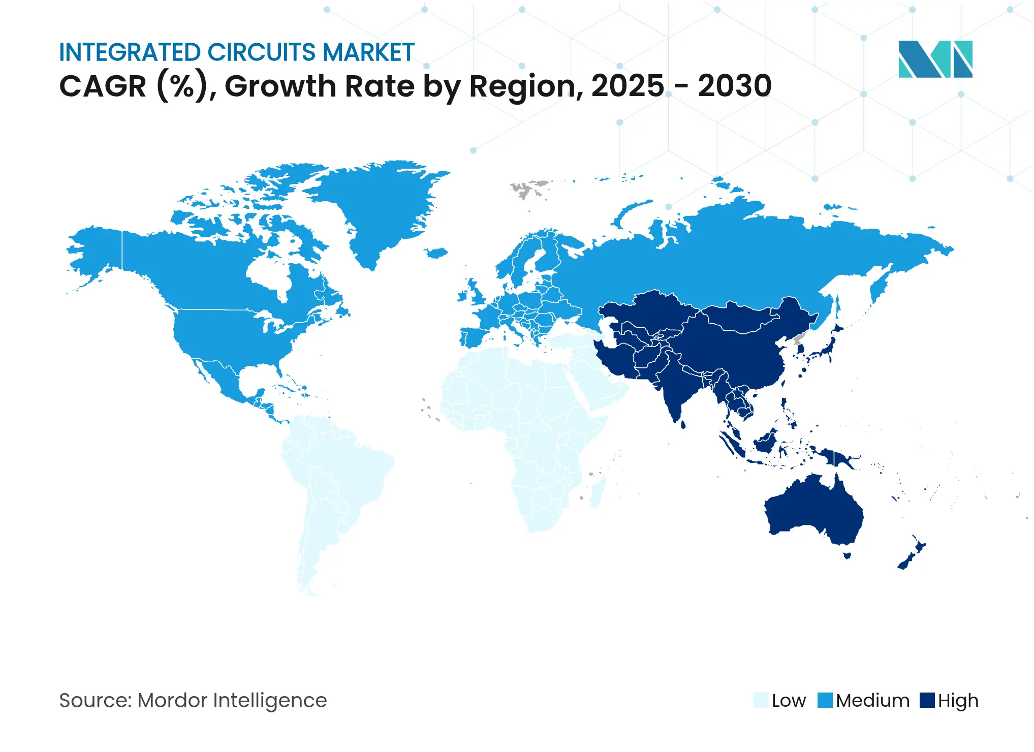
| Fastest Growing Market | Asia-Pacific |
| Largest Market | Asia-Pacific |
| Market Concentration | Medium |
Major Players *Disclaimer: Major Players sorted in no particular order. Image © Mordor Intelligence. Reuse requires attribution under CC BY 4.0. |
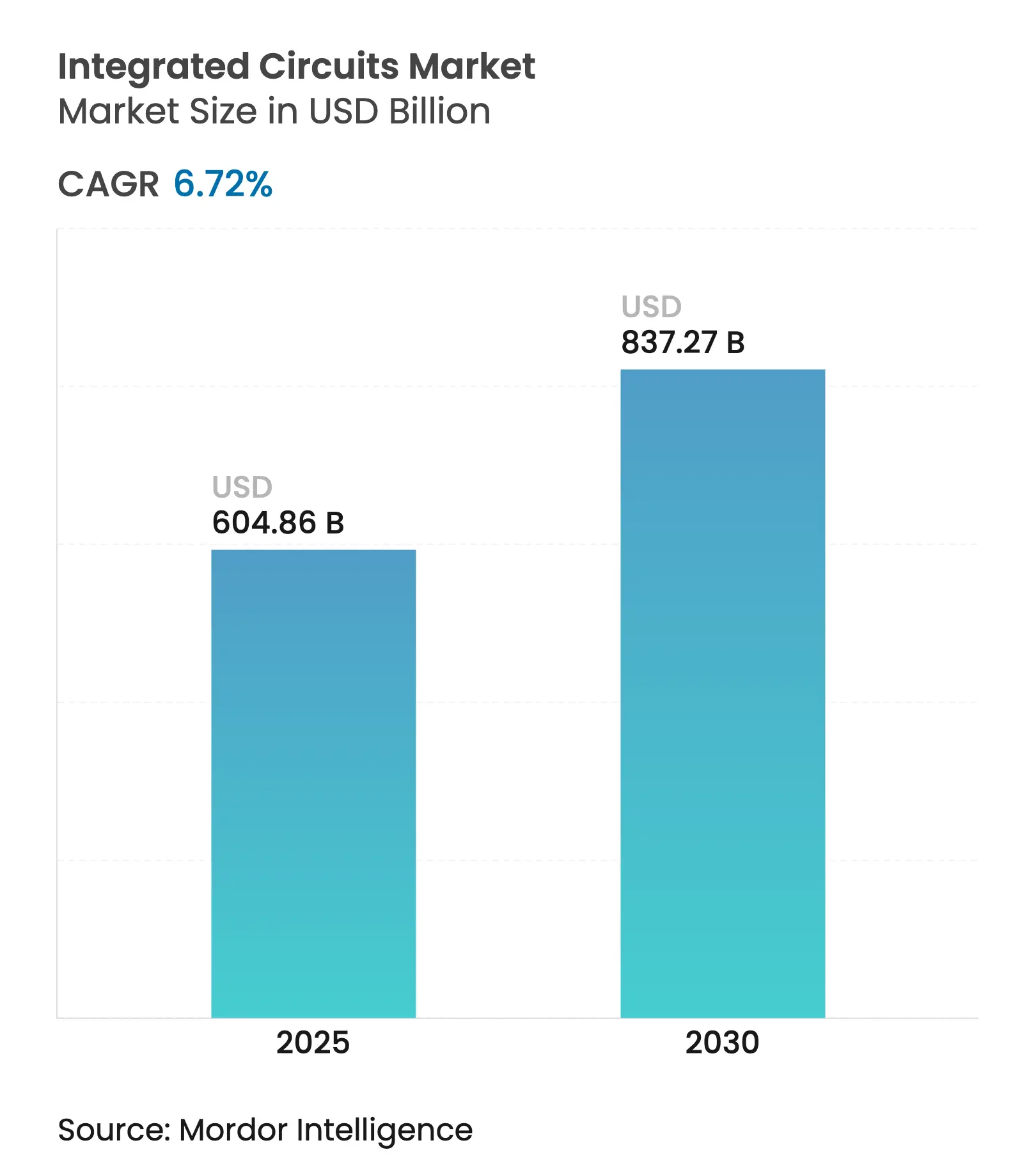
The integrated circuits market size stood at USD 604.86 billion in 2025 and is forecast to reach USD 837.27 billion by 2030, advancing at a 6.72% CAGR. Sellers are pivoting from traditional consumer electronics toward AI-optimised computing, electrified vehicles, and advanced-node packaging that raise value per wafer. Demand for high-bandwidth memory (HBM) and AI GPUs is tightening capacity at leading-edge foundries, while the CHIPS Act and similar incentives are redrawing the global investment map. Automotive electrification is doubling semiconductor content per vehicle and spurring power-device innovation, whereas sovereignty programmes in the United States and Europe are expanding domestic fab footprints. Supply-chain resilience has become a competitive differentiator as export controls reshape equipment flows and encourage regional diversification.
Key Report Takeaways
Drivers Impact Analysis
| Driver | (~) % Impact on CAGR Forecast | Geographic Relevance | Impact Timeline | |||
|---|---|---|---|---|---|---|
Acceleration
of AI-optimised data-centre processor roll-outs in North America and China
Acceleration
of AI-optimised data-centre processor roll-outs in North America and China
| +2.8% | North America & China; spillover to APAC | Short term (≤ 2 years) |
(~)
% Impact on CAGR Forecast
:
+2.8%
|
Geographic
Relevance
:
North
America & China; spillover to APAC
|
Impact
Timeline
:
Short
term (≤ 2 years)
|
Electrification
and ADAS roadmaps are raising per-vehicle IC content for global OEMs
Electrification
and ADAS roadmaps are raising per-vehicle IC content for global OEMs
| +1.9% | Global; early gains in Europe, North America, China | Medium term (2-4 years) | |||
CHIPS
and similar sovereignty acts are triggering multi-billion-dollar foundry
expansion in the US and EU
CHIPS
and similar sovereignty acts are triggering multi-billion-dollar foundry
expansion in the US and EU
| +1.4% | US & EU: indirect benefits to allies | Long term (≥ 4 years) | |||
5G/6G
baseband and RF front-end complexity boosting mixed-signal IC demand in Asia
5G/6G
baseband and RF front-end complexity boosting mixed-signal IC demand in Asia
| +1.2% | APAC core; global telecom spillover | Medium term (2-4 years) | |||
Growth
of industrial IoT retrofits driving high-reliability analog IC consumption in
Europe
Growth
of industrial IoT retrofits driving high-reliability analog IC consumption in
Europe
| +0.8% | Europe & North America; emerging markets | Medium term (2-4 years) | |||
Rising
adoption of chiplet and advanced-packaging architectures is enhancing value
per wafer
Rising
adoption of chiplet and advanced-packaging architectures is enhancing value
per wafer
| +1.1% | Global, led by Taiwan & Korea | Short term (≤ 2 years) | |||
| Source: Mordor Intelligence | ||||||
Acceleration of AI-optimised data-centre processor roll-outs in North America and China
Hyperscalers broadened AI system demand, shifting the mix toward high-performance GPUs, custom accelerators, and HBM stacks. NVIDIA’s Blackwell-generation GPUs and AMD’s Instinct MI300 expanded compute density while pushing TSV-based memory bandwidth requirements. Foundries in Taiwan and Korea lengthened CoWoS and FOWLP lead times, prompting capacity additions and new substrate partnerships. Cloud providers such as Amazon and Microsoft pressed ahead with custom silicon to lower inference cost per watt, intensifying the migration to application-specific designs. North American fab expansions and favourable tax credits compressed time-to-volume for new AI parts, sustaining a robust order pipeline through 2026.
Electrification and ADAS roadmaps raising per-vehicle IC content for global OEMs
Battery electric vehicles and Level-2+ driver-assistance features have elevated silicon demand across power, sensing, and compute domains. Average semiconductor bill-of-materials value per car climbed above USD 900 in 2025 and is on track to reach USD 1,200 by 2030.[1]Economic Times, “Cost of semiconductor chips per vehicle to double to USD 1200 by 2030,” indiatimes.com The shift toward zonal architectures spurred the uptake of centralised domain controllers requiring high-density memory and high-speed SerDes. Infineon, NXP, and STMicroelectronics deepened investments in silicon carbide MOSFETs and 28 nm automotive MCUs to capture next-generation e-powertrain sockets. OEM preference for secure, over-the-air-updatable controllers has made functional-safety certifications and long-life process nodes strategic necessities for suppliers.
CHIPS and similar sovereignty acts triggering multi-billion-dollar foundry expansion in the US and EU
Government grants and investment tax credits accelerated greenfield fabs in Arizona, Ohio, Idaho, and Saxony. TSMC committed more than USD 65 billion across three Arizona sites to supply 2 nm and 3 nm wafers locally. Micron allocated USD 50 billion for advanced DRAM and NAND capacity in Idaho and New York, targeting a 10% US share of leading-edge memory by 2035. In Europe, onsemi selected the Czech Republic for a USD 2 billion vertically integrated silicon-carbide plant, supporting regional electrification goals. These programmes aim to mitigate geopolitical risk, shorten supply chains, and nurture a skilled semiconductor workforce over the next decade.
5G/6G baseband and RF front-end complexity boosting mixed-signal IC demand in Asia
The transition toward 5G-Advanced and early 6G prototypes pushed handset makers and network OEMs to integrate more filters, tuners, and power amplifiers. Qualcomm expanded its RF front-end portfolio into automotive and industrial segments, leveraging integrated connectivity platforms. Design houses across Taiwan, India, and South Korea ramped up GaAs and GaN power amplifier volumes to meet massive MIMO radio requirements. Fixed-wireless-access deployments in Europe and North America boosted demand for ASIC baseband solutions from Asian fabless suppliers. Wi-Fi 7 client chipsets entered pilot production, creating incremental orders for 28 nm mixed-signal wafers at mainland Chinese foundries.
Restraints Impact Analysis
| Restraint | (~) % Impact on CAGR Forecast | Geographic Relevance | Impact Timeline | |||
|---|---|---|---|---|---|---|
EUV
lithography tool lead-times (> 18 months) limiting sub-7 nm capacity ramp
EUV
lithography tool lead-times (> 18 months) limiting sub-7 nm capacity ramp
| −1.8% | Global, concentrated in advanced foundries | Medium term (2-4 years) |
(~)
% Impact on CAGR Forecast
:
−1.8%
|
Geographic
Relevance
:
Global,
concentrated in advanced foundries
|
Impact
Timeline
:
Medium
term (2-4 years)
|
Escalating
advanced-node mask-set costs (> USD 0.6 million) deterring start-up
tape-outs
Escalating
advanced-node mask-set costs (> USD 0.6 million) deterring start-up
tape-outs
| −1.2% | Global; heavily impacts fabless start-ups | Long term (≥ 4 years) | |||
US-China
export controls restricting EDA and equipment supply to Chinese foundries
US-China
export controls restricting EDA and equipment supply to Chinese foundries
| −1.5% | China: secondary impact on global supply chains | Medium term (2-4 years) | |||
| Source: Mordor Intelligence | ||||||
EUV lithography tool lead-times (> 18 months) limiting sub-7 nm capacity ramp
ASML’s limited shipment slots for High-NA EUV systems constrained foundry roadmaps, forcing multi-fab customers to prioritise allocation toward flagship nodes. Equipment price points above USD 360 million per scanner raised capital-intensity ratios and extended return-on-investment horizons. TSMC, Samsung, and Intel optimised existing EUV fleets through higher wafer-per-day utilisation, but incremental supply lagged surging AI logic demand. Delay in next-generation pellicles and mask infrastructure exacerbated the bottleneck, compelling some design houses to tape out at mature nodes for interim products.
US-China export controls restricting EDA and equipment supply to Chinese foundries
Washington’s tightened Foreign Direct Product Rule in December 2024 curtailed the flow of advanced etch, deposition, and design software into China, slowing the domestic migration below 14 nm. In response, Chinese toolmakers accelerated localisation, while Beijing issued export bans on gallium and germanium compounds critical to compound-semiconductor production. Tier-1 Chinese fab customers redirected some orders to local foundries, but back-end optical inspection and high-speed lithography gaps remained. Multinational firms with fabs in China began contingency planning for dual-sourcing to Korea and ASEAN nations, raising operating complexity and inventory buffers.
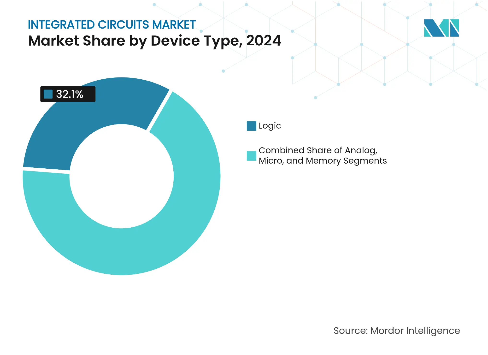
By Device Type: Memory outpaces logic on AI bandwidth needs
Memory IC revenue expanded faster than any other category as AI training clusters required wider HBM stacks and higher DDR5 densities. Logic ICs still generated the largest sales pool in 2024 on the strength of CPU, GPU, and SoC demand across consumer and industrial systems. However, the integrated circuits market size for memory is projected to expand at a 12.2% CAGR, underlining the strategic pivot toward data-centric architectures. Suppliers invested in hybrid-bonded 3D DRAM to minimise package height while boosting channel width, enabling next-generation accelerators to feed thousands of compute cores efficiently. Adjacent analogue power-management devices experienced halo growth, ensuring stable voltage rails for the denser memory hierarchy.
Second-tier categories, including analogue signal-chain ICs and microcontrollers, remained indispensable for edge and motor-control tasks in automotive and factory automation. Edge-AI microcontrollers incorporating neural-network accelerators found adoption in smart sensors that demanded low latency and battery efficiency. Although more cyclical in nature, these devices provide resilience to the overall integrated circuits market during smartphone or PC downturns.
Note: Segment shares of all individual segments available upon report purchase
By Product Type: Custom ASICs displace some general-purpose volumes
In 2024, general-purpose ICs delivered 60.3% of sales due to ubiquity across many verticals. Yet hyperscalers’ pursuit of workload-specific efficiency pushed application-specific ICs toward an 8.7% CAGR through 2030. Each custom accelerator tuned for transformer inference or network security replaced multiple off-the-shelf processors, shrinking rack power draw. The integrated circuits market share for application-specific parts climbed most sharply in cloud data-centre build-outs that prize predictable latency over multi-tenant flexibility. Vendors responded with configurable chiplet platforms that shorten time-to-tape-out while preserving architectural differentiation.
General-purpose processors continued to evolve instruction-set extensions, cache hierarchies, and vector units to counter specialised chips. Their sheer shipment scale sustained healthy wafer-start volumes at 5 nm and 3 nm, underpinning economies of scale for foundries. Emerging RISC-V ecosystems added competition, offering license-free designs that encourage regional self-reliance, particularly in Asia.
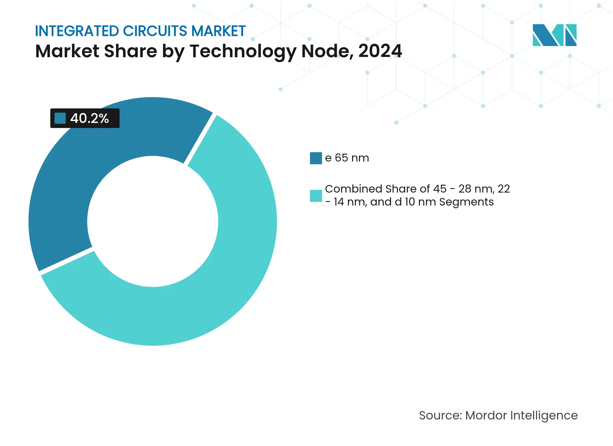
By Technology Node: ≤ 10 nm nodes deliver performance leadership
Foundries raised capital budgets to migrate premium mobile and data-centre products to 3 nm and below, even as ≥ 65 nm processes handled high-volume, cost-sensitive applications. The ≥ 65 nm class remained the largest revenue contributor in 2024 because of longevity in power, automotive, and display drivers. Nonetheless, the ≤ 10 nm tier is projected to log a 12.1% CAGR, reflecting sustained appetite for transistor-density scaling to support AI workloads. The integrated circuits market size tied to sub-10 nm capacity is expected to rise faster than overall industry averages between 2025-2030, buoyed by demand for 2 nm gate-all-around architectures.
Intermediate nodes such as 22FDX and 14 nm fin-FETs preserved value for mixed-signal and RF products that benefit from improved leakage without extreme lithography costs. Many automotive suppliers locked long-term supply agreements on these nodes to balance longevity, safety ratings, and total cost of ownership.
By Wafer Size: 300 mm remains dominant while 450 mm pilots gain traction
Seventy-two percent of 2024 wafer starts were processed on 300 mm lines, owing to mature equipment ecosystems and optimised fab utilisation. Capital expenditure plans indicate further 300 mm expansions in the Americas and Japan to serve AI accelerators and HBM production.[2]SEMI, “Global Semiconductor Industry Plans to Invest USD 400 Billion in 300 mm Fab Equipment,” semi.org However, 450 mm feasibility studies revived as cost-per-die analyses turned favourable for large-area logic dies. Pilot tools shipping after 2027 could elevate throughput without a proportional rise in labour or clean-room footprint, lifting gross-margin potential.
Meanwhile, 200 mm fabs retained strategic importance for analogue, power, and MEMS devices, where design shrink delivers minimal performance upside. The SkyWater acquisition of Infineon’s Austin facility underscored continuing demand for 65 nm-to-130 nm nodes in defence, industrial, and secure-ID applications.
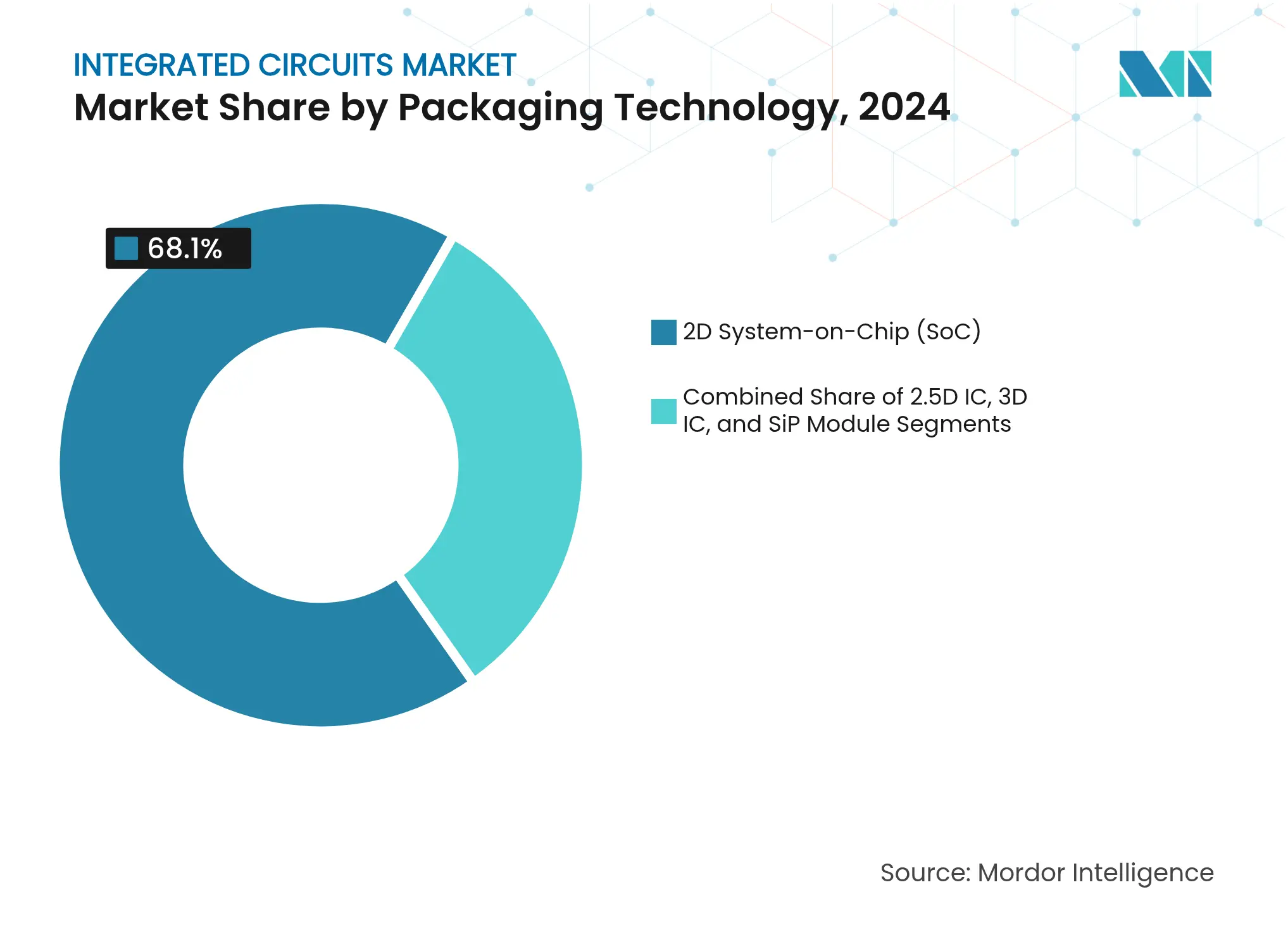
By Packaging Technology: 3D integration redefines system architecture
Traditional 2D system-on-chip approaches, while still prevalent, faced performance ceilings linked to reticle size and power density. Chiplet-based 3D ICs used hybrid bonding and backside power delivery to shorten interconnect distances and slash latency, powering accelerators that deliver petaflop-class compute in a single socket. Integrated circuits market size revenue from 3D IC packaging is projected to grow at 14.4% CAGR, the highest among packaging formats. Co-packaged optics advanced in parallel, targeting 800 Gbps and 1.6 Tbps switch ASIC roadmaps that cannot accommodate conventional pluggable modules.
2.5D interposers offered a transitional step, enabling disaggregation of logic and memory using silicon bridges while avoiding full 3D stacking costs. System-in-Package modules kept momentum in wearables and IoT nodes, where board area and battery life remain premium constraints.
By End-User Industry: Automotive narrows the gap with consumer electronics
Consumer devices still generated one-third of 2024 revenue, but unit shipments plateaued as handset replacement cycles lengthened. Automotive electronics is projected to record a 10.8% CAGR, the fastest among end markets, propelled by electrified drivetrains and Level-2+ autonomy. Memory footprints per vehicle are forecast to exceed 278 GB by 2026, with multiple HBM dies entering zonal and central compute domains. The integrated circuits industry also benefited from industrial automation upgrades, where predictive maintenance and machine vision require edge-AI inference silicon.
Government and defence programmes prioritised secure, long-lifecycle components, stimulating demand for radiation-hardened FPGAs and trusted-foundry ASICs. Communication infrastructure spent steadily on 5G Massive-MIMO radios and began trials on Open-RAN split architectures that employ merchant silicon for baseband processing.
Asia-Pacific retained 63.2% of global revenue in 2024, anchored by Taiwan’s foundry leadership, South Korea’s memory dominance, and China’s captive demand for domestic chips. Regional CAGR of 8.1% through 2030 is driven by aggressive capital formation, design-ecosystem maturation, and state incentives. Chinese firms accelerated self-reliance programmes, fostering local lithography and EDA suppliers despite export-control hurdles. Taiwan’s TSMC scaled Arizona knowledge back into its Hsinchu headquarters, safeguarding future technology nodes. South Korea diversified into chiplet and AI accelerator design to offset DDR and NAND cyclicality, while Japan leveraged materials and equipment strength to secure a resilient position in the integrated circuits market.
North America ranked second by value after deploying more than USD 540 billion of announced fab investments since 2022. Domestic HBM and logic capacity gained momentum as the CHIPS Act disbursed direct funding to multiple projects. Texas emerged as a mixed-node hub following SkyWater’s 200 mm acquisition and Samsung’s ongoing 4 nm ramp near Austin. The region also concentrated advanced packaging R&D, with glass-core substrates and CoWoS capacity under construction to alleviate Asian bottlenecks.
Europe pursued strategic autonomy through the European Chips Act, offering grants to attract power-device and RF front-end production. onsemi’s silicon-carbide vertical integration in the Czech Republic exemplified the continent’s focus on electrification value chains.[3]onsemi, “onsemi selects Czech Republic for silicon-carbide production,” onsemi.com Germany and France funded research alliances on 2 nm gate-all-around technologies, while the United Kingdom repositioned Newport Wafer Fab for automotive Grade-0 and industrial markets. Combined, these programmes target a mid-single-digit percentage increase in Europe’s slice of global wafer starts by decade-end.
Market Concentration
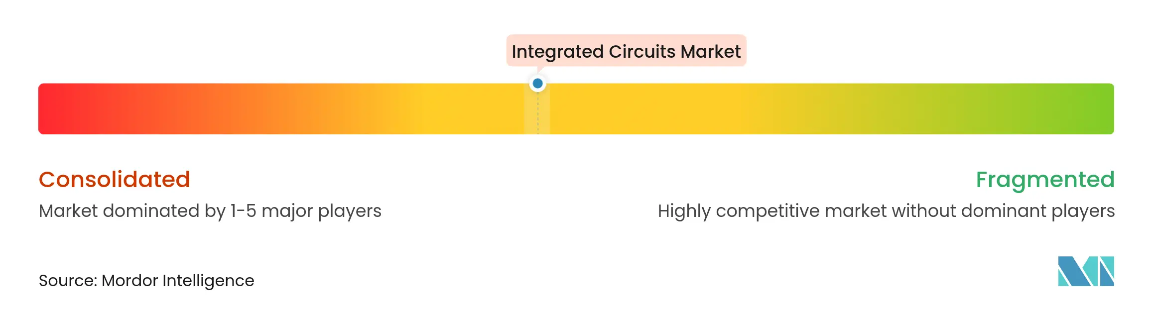
The competitive arena tightened around a handful of companies controlling advanced nodes, HBM supply, and cutting-edge packaging. TSMC and Samsung offered the only commercial 3 nm capacity in 2025, with Intel re-entering the foundry race on its Intel 16 and Intel 3 processes. SK Hynix and Micron captured most HBM3e and early HBM4 demand, locking long-term supply agreements with hyperscalers. NVIDIA sustained roughly 80% revenue share in AI GPUs, but AMD and custom ASIC vendors gained ground in inference workloads, diversifying the supplier base.[4]Octopart, “NVIDIA Holds 80% AI Chip Market Share,” octopart.com
Acquisition activity centred on capability fill-ins: Nokia agreed to buy Infinera for USD 2.3 billion to bolster optics; onsemi purchased Qorvo’s SiC JFET line for USD 115 million to expand high-efficiency power portfolios; and SkyWater took over Infineon’s Austin fab to secure domestic trusted-foundry capacity. Equipment vendors such as ASML retained a near-monopoly on EUV scanners, giving the Netherlands-based firm disproportionate pricing power. Start-ups seized niches in chiplet interconnect IP and lithography-independent patterning, hoping to ride the industry’s heterogeneous-integration wave.
Geopolitics added another competitive layer. US-origin EDA restrictions spurred Chinese firms to co-develop open-source design flows, reducing dependence on proprietary Western tools. Meanwhile, gallium and germanium export curbs by China prompted Western IDM and OEM buyers to dual-source from Australia and Europe. Supply-chain optionality became a board-level metric for risk management, influencing long-term sourcing and partnership decisions.

*Disclaimer: Major Players sorted in no particular order
1. INTRODUCTION
2. RESEARCH METHODOLOGY
3. EXECUTIVE SUMMARY
4. MARKET LANDSCAPE
5. MARKET SIZE AND GROWTH FORECASTS (VALUE AND VOLUME)
6. COMPETITIVE LANDSCAPE
7. MARKET OPPORTUNITIES AND FUTURE OUTLOOK
An Integrated Circuit (IC) is also called a microchip, microelectronic circuit, or chip, an assembly of electronic components fabricated as a single unit. These units are integrated with miniaturized with active devices (e.g., diodes, transistors, etc.) and passive devices (e.g., resistors, capacitors, etc.), and their interconnections are established on a thin substrate of semiconductor material (usually silicon).
The Global Integrated Circuits Market is Segmented by Type (Digital IC, Analog IC, Mixed-Signal IC), Product Type (General-Purpose IC, Application-Specific IC), End-user Industry (Consumer Electronics, Automotive, IT & Telecommunications, Manufacturing, and Automation), and Geography.
Pricing Strategy for Semiconductor Components
3 Min Read
Accelerating Additive Manufacturing Adoption in India
3 Min Read
Unlocking Growth in India’s Luxury Beauty & Skincare Market
3 Min Read
When decisions matter, industry leaders turn to our analysts. Let’s talk.