
EUV Photoresist Materials Market Size and Share
Market Overview
| Study Period | 2020 - 2031 |
|---|---|
| Market Size (2026) | USD 378.18 Million |
| Market Size (2031) | USD 759.29 Million |
| Growth Rate (2026 - 2031) | 14.96 % |
| Fastest Growing Market | North America |
| Largest Market | Asia-Pacific |
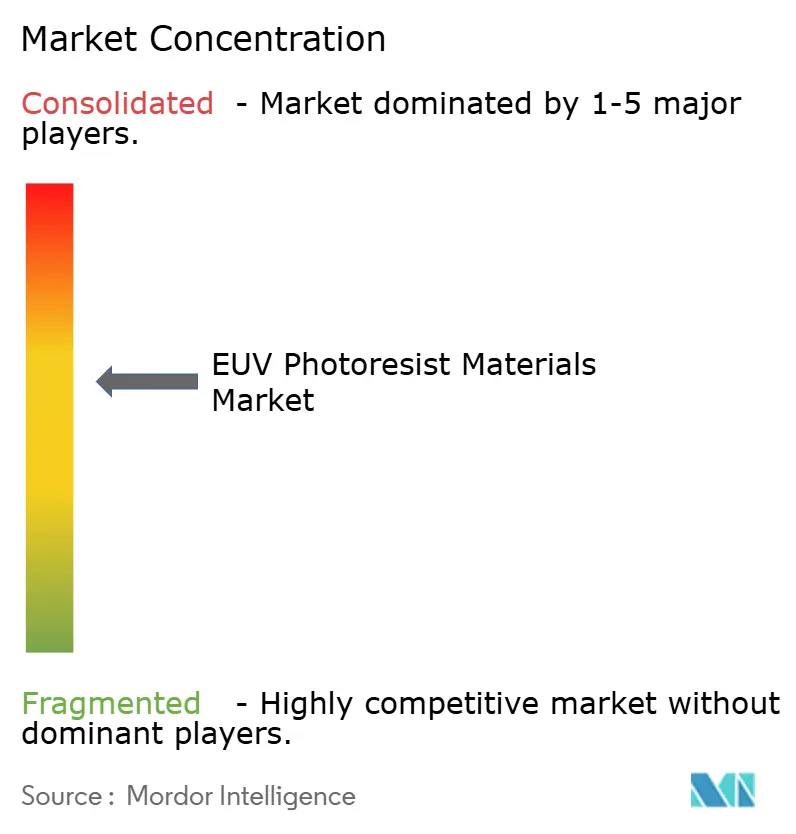
| Market Concentration | Medium |
Major Players *Disclaimer: Major Players sorted in no particular order Image © Mordor Intelligence. Reuse requires attribution under CC BY 4.0. | |
EUV Photoresist Materials Market Analysis by Mordor Intelligence
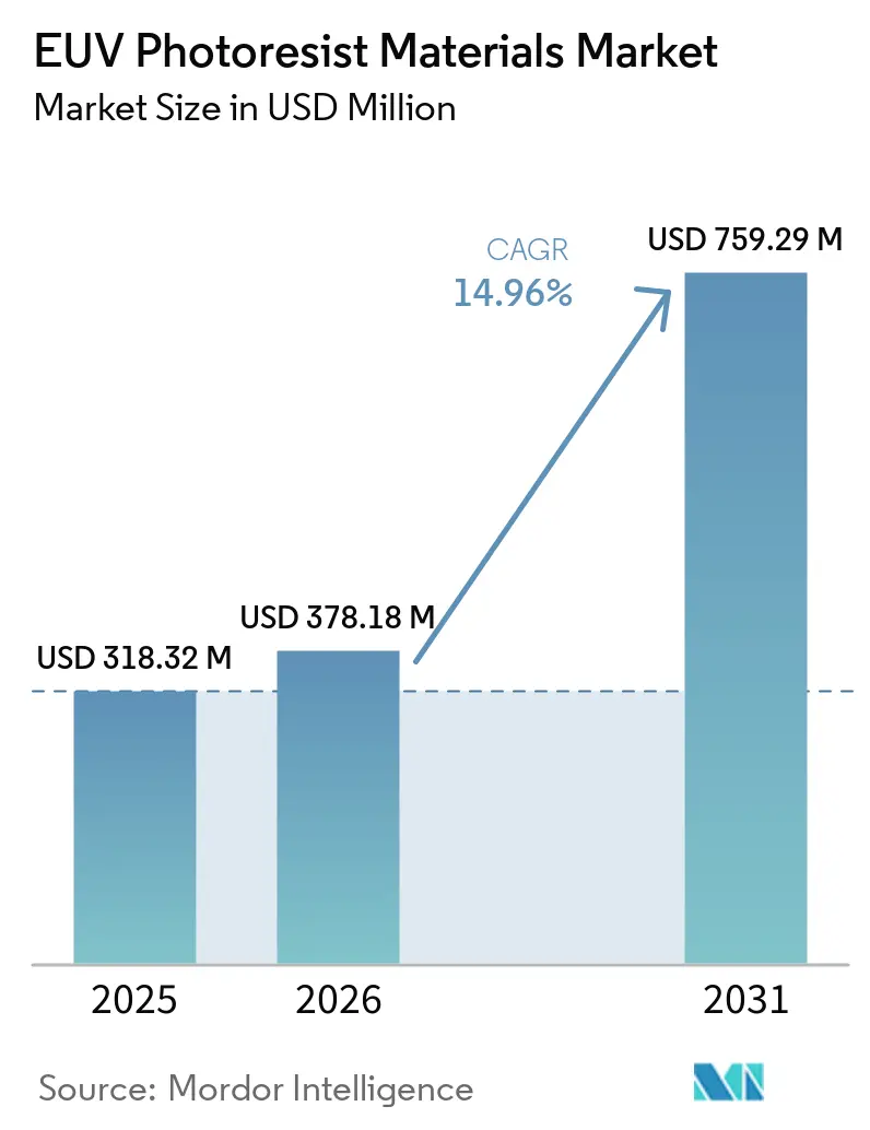
The EUV Photoresist Materials Market size was valued at USD 318.32 million in 2025 and is estimated to grow from USD 378.18 million in 2026 to reach USD 759.29 million by 2031, at a CAGR of 14.96% during the forecast period (2026-2031). Robust wafer demand for 3-nanometer-and-below logic, escalating shipments of artificial-intelligence accelerators and high-bandwidth memory, and government subsidies that underwrite on-shore lithography investments are the primary forces behind this trajectory. Chemically amplified resists maintain scale advantages today, yet metal oxide and dry chemistries are winning share in risk-production for 2-nanometer nodes because they deliver lower line-edge roughness and higher photon efficiency. Foundries continue to dominate early adoption because they can amortize extreme-ultraviolet scanner costs across multiple customers, while integrated device manufacturers accelerate spending under sovereign-chip programs. Tight scanner supply and emergent environmental regulations raise capital and compliance costs, but they also speed the transition to high-efficiency resists that stretch tool productivity.
Key Report Takeaways
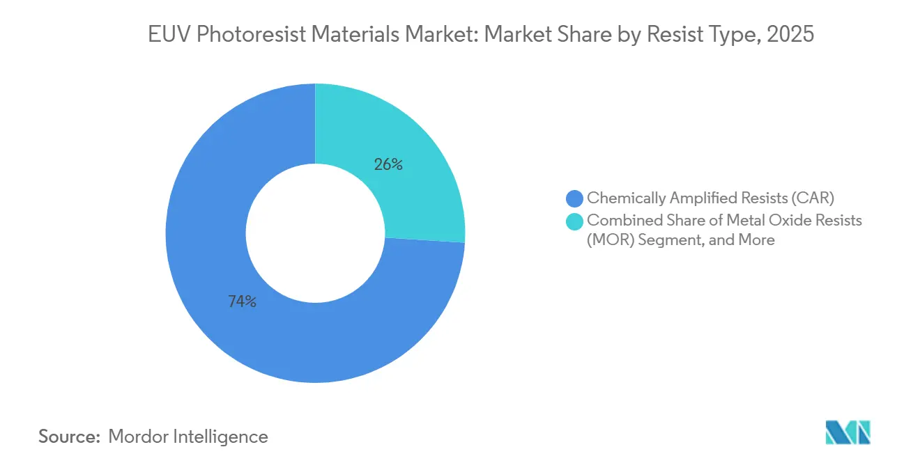
- By resist type, chemically amplified resists led with 74.0% revenue share of the EUV photoresist materials market in 2025, whereas metal oxide resists are forecast to advance at an 18.4% CAGR through 2031, the fastest among all chemistries.
- By node compatibility, advanced nodes spanning 5 nanometers to 7 nanometers captured 57.0% of the EUV photoresist materials market share in 2025, while leading-edge nodes at 3 nanometers and below are projected to grow at a 19.8% CAGR over 2026-2031.
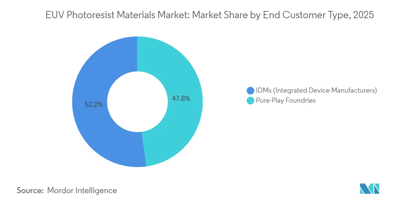
- By end customer type, pure-play foundries accounted for 47.8% of the EUV photoresist materials market in 2025, yet integrated device manufacturers are poised to grow at 17.6% annually as sovereign-chip mandates fund on-shore capacity.
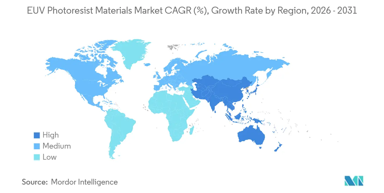
- By geography, Asia-Pacific commanded 37.7% of the EUV photoresist materials market in 2025 revenue, but North America is expected to post the highest regional growth at 19.2% CAGR, buoyed by CHIPS Act disbursements.
Note: Market size and forecast figures in this report are generated using Mordor Intelligence’s proprietary estimation framework, updated with the latest available data and insights as of January 2026.
Market Trends and Insights
Drivers Impact Analysis of EUV Photoresist Materials Market*
| Driver | (~) % Impact on CAGR Forecast | Geographic Relevance | Impact Timeline |
|---|---|---|---|
| Rapid EUV Adoption for ≤3 nm Nodes | +4.20% | Global, led by Taiwan, South Korea, United States | Medium term (2–4 years) |
| Expansion of AI Accelerator Fab Capacity | +3.80% | Asia-Pacific core, North America expansion | Short term (≤ 2 years) |
| Dominance of Pure-Play Foundries in Leading-Edge Logic | +2.60% | Taiwan, South Korea, Arizona and Texas | Medium term (2–4 years) |
| Government Subsidies for On-shore Advanced Nodes | +2.10% | North America, Europe, South Korea | Long term (≥ 4 years) |
| Supply Chain Localization Incentives | +1.50% | United States, European Union, South Korea | Long term (≥ 4 years) |
| Yield Gains from Metal Oxide Dry Resists | +0.80% | Global, early adoption in memory fabs | Medium term (2–4 years) |
| Source: Mordor Intelligence | |||
Rapid EUV Adoption For ≤3 Nm Nodes
The migration from immersion deep-ultraviolet multi-patterning to single-pass extreme-ultraviolet exposure eliminates resolution ceilings at advanced geometries. TSMC now patterns more than 20 layers with EUV on its 2-nanometer process, almost twice the count used at 3-nanometer, which reduces total masks and process steps.[1]Intel integrates high-NA tools that achieve 8-nanometer resolution, enabling single-exposure patterning that boosts yield and slashes defect density. Samsung’s second-generation 2-nanometer technology reached 70% yields after resist optimizations cut line-edge roughness below 1.5 nanometers. Although each high-NA scanner costs about USD 350 million, fabs recover the differential by eliminating multi-patterning loops and realizing faster cycle times.[2]
Expansion Of AI Accelerator Fab Capacity
Artificial-intelligence chips consumed most 3-nanometer wafer allocations in 2025, stretching lead times past 50 weeks. NVIDIA alone booked more than half of TSMC’s advanced packaging output in 2026, swelling demand for EUV photoresist materials market volumes at both wafer and package levels.[3] Capacity additions in Arizona, Taylor, and Ohio, backed by USD 19.2 billion in combined CHIPS Act grants and loans, pull forward resist orders even before the fabs are fully ramped.[4] With every high-NA scanner absorbing USD 2-3 million of photoresist a year, incremental tool deployments translate directly into material consumption.
Dominance Of Pure-Play Foundries In Leading-Edge Logic
Pure-play foundries benefit from customer diversification and the ability to amortize lithography overhead across many product families. TSMC ended 2026 with 180,000 3-nanometer wafer starts per month and will add 100,000 2-nanometer starts by 2027, guaranteeing scale economies for emerging resist chemistries. Samsung’s gate-all-around roadmap won wins from Qualcomm and Google, broadening the revenue base needed to support rapid chemistry refresh cycles. Foundries also run open innovation platforms that feed process feedback to resist suppliers in real time, shortening qualification loops compared with vertically integrated rivals.
Government Subsidies For On-Shore Advanced Nodes
The United States, South Korea, and the European Union collectively earmarked more than USD 140 billion for lithography-class fabs between 2023 and 2025, lowering the effective cost of scanner procurement and smoothing cash flow for photoresist stocking. Tokyo Ohka Kogyo’s decision to co-locate a new plant in Pyeongtaek and JSR’s R&D expansion in Korea demonstrate how subsidies cascade downstream to material suppliers. The programs also include tax credits for domestic chemical production, creating a structural incentive to regionalize supply chains for the EUV photoresist materials industry.
Restraints Impact Analysis of EUV Photoresist Materials Market*
| Restraint | (~) % Impact on CAGR Forecast | Geographic Relevance | Impact Timeline |
|---|---|---|---|
| Limited EUV Scanner Availability | -2.80% | Global, acute in North America and Europe | Short term (≤ 2 years) |
| Line Edge Roughness Challenges Below 3 nm | -1.90% | Global, most severe at 2 nm and below | Medium term (2–4 years) |
| Environmental Health and Safety Concerns for MOR Chemistries | -0.70% | North America, European Union | Long term (≥ 4 years) |
| High CoO Compared With Immersion DUV | -0.50% | Global, particularly for mature nodes | Medium term (2–4 years) |
| Source: Mordor Intelligence | |||
Limited EUV Scanner Availability
ASML shipped 60 systems in 2025 and plans just over 80 in 2027, yet foundry order books stretch two years ahead. Each delay deprives a fab of up to 15,000 wafers per month, forcing operators to ration photoresist purchases and injecting revenue volatility into the EUV photoresist materials market. Intel’s Ohio complex slipped seven years primarily because of long-cycle high-NA tool deliveries, underscoring how monopoly equipment supply throttles regional diversification. Short-term shortages also amplify the value proposition of metal oxide and dry resists, which raise dose efficiency and stretch throughput per tool.
Line Edge Roughness Challenges Below 3 Nm
At 2-nanometer geometries, line-edge roughness targets fall to 1.5 nanometers, a regime where polymer molecular weight alone can derail yield. Imec showed PFAS-free polymer resists that meet resolution goals only by increasing the dose 20%, which cuts scanner throughput. Metal oxide resists inherently deliver finer edges but remain negative-tone, requiring process redesigns. Industry is experimenting with post-exposure thermal treatments and multi-trigger chemistries, yet every added step erodes the cost savings formerly promised by single-exposure EUV.
*Our forecasts treat driver/restraint impacts as directional, not additive. The impact forecasts reflect baseline growth, mix effects, and variable interactions.
EUV Photoresist Materials Market Segment Analysis
By Resist Type:
Metal Oxide Resists Outpace Polymer IncumbentsMetal oxide resists, anchored by tin-oxide cluster technology, are projected to register the strongest growth, advancing at an 18.4% CAGR through 2031. In 2025, chemically amplified products still dominated the EUV photoresist materials market size because fabs favor proven track compatibility and positive-tone polarity. Adoption momentum shifted in 2026 when Lam Research demonstrated its vapor-phase Aether platform that cuts chemical consumption by up to 25% and achieves single-print patterns below 20 nanometers.
Chemically amplified resists retain economies of scale, yet stochastic defects at sub-3-nanometer nodes compel fabs to pilot alternative chemistries. JSR and Lam Research now offer hybrid workflows that pair vapor deposition with inorganic photosensitizers, signaling a path toward positive-tone metal oxide solutions that could displace polymer incumbents within the forecast horizon. Regulatory moves by the U.S. Environmental Protection Agency and the European Chemicals Agency accelerate this pivot by capping PFAS content, incentivizing suppliers to transition to PFAS-free metal oxide and dry formulations.

By Node Compatibility:
Leading Edge Pulls Resist InnovationAdvanced nodes between 5 nanometers and 7 nanometers delivered 57.0% of 2025 revenue, reflecting the mature installed base of 0.33-NA scanners. However, leading-edge nodes at 3 nanometers and below are forecast to post a 19.8% CAGR, making them the primary engine of both volume and pricing power. The EUV photoresist materials market size commanded by these geometries will expand rapidly as TSMC, Samsung, and Intel ramp high-NA tools that shrink half-pitch down to 8 nanometers.
Because each leading-edge wafer commands 30-50% higher revenue than a 5-nanometer wafer, resist suppliers can charge premiums that double gross margin per liter. Yet rising dose requirements partially offset that benefit, forcing suppliers to refine quantum efficiency above 20 photons per absorbed event. The shift also concentrates demand among suppliers with the depth to qualify formulations in less than 18 months, narrowing viable competition to a handful of Japanese incumbents and two U.S. newcomers.
By End Customer Type:
Integrated Device Manufacturers Narrow The GapPure-play foundries are projected to hold 47.8% of the EUV photoresist materials market share in 2025. This dominance is primarily driven by TSMC’s and Samsung’s combined control over high-volume 3-nanometer production capacity. These foundries benefit from structural advantages, such as the ability to amortize scanner depreciation costs across multiple customers. Additionally, they maintain faster chemistry feedback loops, which enhance their operational efficiency. These factors collectively strengthen their competitive position in the market. As a result, pure-play foundries continue to be a critical force in shaping the EUV photoresist materials landscape.
Integrated device manufacturers (IDMs), however, are narrowing the gap as sovereign-chip programs mitigate risks in their capital plans. For instance, Intel has secured USD 7.86 billion in CHIPS Act grants, which directly subsidize high-NA tools. This financial support reduces payback periods and enhances their ability to purchase resists. Furthermore, vertical integration enables IDMs to tailor resist formulations for proprietary gate-all-around or nanosheet architectures. This capability provides a significant advantage that pure-play foundries cannot replicate without disrupting their standardized process platforms. Consequently, IDMs are positioning themselves as formidable competitors in the EUV photoresist materials market.
Geography Analysis
North America EUV Photoresist Materials Market
North America is projected to record the fastest CAGR at 19.2% during 2026-2031 as CHIPS Act incentives accelerate three mega-fab projects: TSMC Arizona, Samsung Taylor, and Intel Ohio. Once operational, these plants will collectively add more than 400,000 leading-edge wafer starts per month, translating into an additional USD 150-200 million in annual demand for EUV photoresist materials market volumes. Regulations that establish a controlled-use pathway for PFAS in photoresists reduce compliance ambiguity and encourage local production of materials.
APAC EUV Photoresist Materials Market
Asia-Pacific remains the revenue anchor, with a 37.7% share in 2025, as Taiwan and South Korea host more than 60% of the global EUV scanner fleet. Local suppliers benefit from short logistics lanes, while Japanese chemical companies are expanding production in Pyeongtaek and Ibaraki to co-locate with Samsung and TSMC. Although the region maintains its leadership, incremental share gains are likely to moderate as North American capacity scales.
Europe EUV Photoresist Materials Market
Europe trails in absolute size but benefits from the EUR 43 billion European Chips Act, which aims to double the regional semiconductor share by 2030. Imec’s Leuven hub and JSR’s nearby manufacturing base serve as material qualification centers for future high-NA nodes built in Germany and France. Supplier interest is rising because the REACH Annex XV proposal clarifies permissible PFAS thresholds, providing the regulatory certainty needed to green-light capacity additions.
Competitive Landscape
Japanese suppliers, JSR, Tokyo Ohka Kogyo, Fujifilm, and Shin-Etsu Chemical, control the bulk of chemically amplified portfolio revenues, while JSR’s Inpria subsidiary dominates tin-oxide resists that enable the tightest line-edge roughness targets. The arrival of Lam Research’s Aether dry resist in production at a major memory manufacturer proves that etch-resistant vapor coatings can migrate from pilot to high-volume in fewer than 24 months, challenging wet-track incumbents.
Cross-licensing between JSR and Lam Research underscores a strategic pivot toward process-level differentiation rather than chemistry alone. By combining dry deposition with metal oxide patterning, they cut dose while preserving resolution, creating a defensible niche against pure polymer suppliers. Tokyo Ohka Kogyo’s investment in Irresistible Materials opens a second disruption vector, multi-trigger molecular resists that are PFAS-free and potentially positive-tone, addressing both regulatory risk and integration friction.
White-space opportunities focus on developing positive-tone metal oxide resists and scaling PFAS-free polymers that do not sacrifice sensitivity. Chinese institutes are attempting to localize supply, but Japanese firms still command process know-how and customer trust, preserving a moderate concentration dynamic in the EUV photoresist materials market.
EUV Photoresist Materials Industry Leaders
-
JSR Corporation
-
Tokyo Ohka Kogyo Co., Ltd.
-
Fujifilm Holdings Corporation
-
Shin-Etsu Chemical Co., Ltd.
-
Brewer Science, Inc.
- *Disclaimer: Major Players sorted in no particular order
EUV Photoresist Materials Market Companies Covered in this Report
- JSR Corporation
- Tokyo Ohka Kogyo Co., Ltd. (TOK)
- Fujifilm Holdings Corporation
- Shin-Etsu Chemical Co., Ltd.
- Brewer Science, Inc.
- Inpria Corporation (JSR)
- Merck KGaA (AZ Electronic Materials)
- DuPont de Nemours, Inc.
- Sumitomo Chemical Co., Ltd.
- Dongjin Semichem Co., Ltd.
- Avantama AG
- Lam Research Corporation
- LG Chem Ltd.
- Arkema S.A.
- Tokyo Electron Limited (dry resist co-development)
- S&S Tech Corporation
- Kayaku Advanced Materials, Inc.
- GlobalWafers Co., Ltd.
- Integrated Micro Materials LLC
- Beijing Institute of Chemical Engineering (BICEM)
Recent Industry Developments in EUV Photoresist Materials Market
- March 2026: Tokyo Ohka Kogyo purchased land in Fukushima for a new domestic photoresist plant valued at JPY 1.5 billion (USD 10 million).
- February 2026: Tokyo Ohka Kogyo invested in Irresistible Materials to accelerate multi-trigger, PFAS-free resist development for high-NA applications.
- January 2026: Lam Research announced volume adoption of its Aether dry resist by a leading memory maker, marking the first commercial vapor-phase EUV resist deployment.
- September 2025: JSR and Lam Research entered a cross-licensing deal linking dry deposition with metal oxide patterning for 2 nanometer nodes.
Global EUV Photoresist Materials Market Report Scope
The EUV Photoresist Materials Market is Segmented by Resist Type (Chemically Amplified Resists, Metal Oxide Resists, and Non-Chemically Amplified and Dry Resists), Node Compatibility (Leading Edge 3 nm and Below, and Advanced Nodes 5 nm to 7 nm), End Customer Type (Pure-Play Foundries, and IDMs), and Geography (North America, Europe, Asia-Pacific, and Rest of the World). Market Forecasts are Provided in Terms of Value (USD).
Segmentation Overview
| Chemically Amplified Resists (CAR) |
| Metal Oxide Resists (MOR) |
| Non-Chemically Amplified / Dry Resists |
| Leading Edge (3 nm and Below) |
| Advanced Nodes (5 nm-7 nm) |
| Pure-Play Foundries |
| IDMs (Integrated Device Manufacturers) |
| North America | United States |
| Canada | |
| Mexico | |
| Europe | United Kingdom |
| Germany | |
| France | |
| Italy | |
| Rest of Europe | |
| Asia-Pacific | China |
| Japan | |
| India | |
| South Korea | |
| Rest of Asia-Pacific | |
| Rest of the World |
| By Resist Type | Chemically Amplified Resists (CAR) | |
| Metal Oxide Resists (MOR) | ||
| Non-Chemically Amplified / Dry Resists | ||
| By Node Compatibility | Leading Edge (3 nm and Below) | |
| Advanced Nodes (5 nm-7 nm) | ||
| By End Customer Type | Pure-Play Foundries | |
| IDMs (Integrated Device Manufacturers) | ||
| By Geography | North America | United States |
| Canada | ||
| Mexico | ||
| Europe | United Kingdom | |
| Germany | ||
| France | ||
| Italy | ||
| Rest of Europe | ||
| Asia-Pacific | China | |
| Japan | ||
| India | ||
| South Korea | ||
| Rest of Asia-Pacific | ||
| Rest of the World | ||
Key Questions Answered in the Report
What is the current EUV photoresist materials market size and how fast is it growing?
The EUV photoresist materials market size is USD 378.18 million in 2026 and is forecast to reach USD 759.29 million by 2031, reflecting a 14.96% CAGR over 2026-2031.
Which resist type is gaining share the fastest?
Metal oxide resists are forecast to expand at an 18.4% CAGR through 2031 because they deliver lower line-edge roughness and higher photon absorption efficiency.
Why are North American fabs important to future demand?
CHIPS Act funding exceeding USD 19 billion is underwriting mega-fab projects for TSMC, Samsung and Intel, which will materially lift North American demand for EUV photoresist materials once online.
How does limited EUV scanner supply affect material consumption?
Scanner shortages delay fab ramps, causing uneven resist purchasing; however, installed tools run at full utilization, meaning any incremental scanner shipment immediately absorbs USD 2-3 million of resist per year.
Which companies currently lead the market?
JSR, Tokyo Ohka Kogyo, Fujifilm and Shin-Etsu Chemical dominate chemically amplified resists, while JSRs Inpria subsidiary commands metal oxide resists and Lam Research leads in dry resist technology.
What environmental regulations influence product development?
The U.S. Environmental Protection Agency’s tiered PFAS framework and the European Chemicals Agency’s Annex XV proposal set strict PFAS thresholds, pushing suppliers toward PFAS-free and metal oxide chemistries.