
Size and Share of Photoresist and EUV Photochemicals Market For DRAM Manufacturing
Market Overview
| Study Period | 2020 - 2031 |
|---|---|
| Market Size (2026) | USD 1.18 Billion |
| Market Size (2031) | USD 2.05 Billion |
| Growth Rate (2026 - 2031) | 11.68 % |
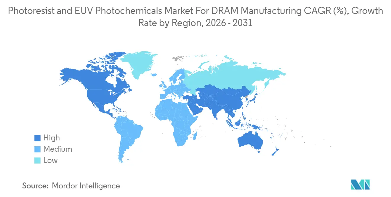
| Fastest Growing Market | North America |
| Largest Market | Asia-Pacific |
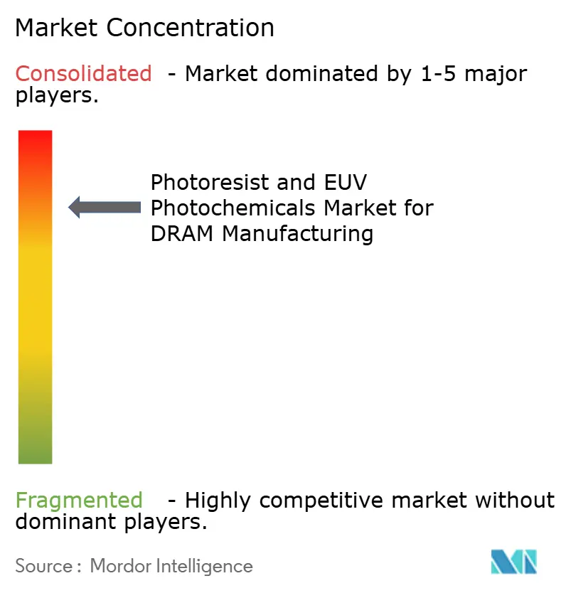
| Market Concentration | High |
Major Players *Disclaimer: Major Players sorted in no particular order Image © Mordor Intelligence. Reuse requires attribution under CC BY 4.0. | |
Analysis of Photoresist and EUV Photochemicals Market For DRAM Manufacturing by Mordor Intelligence
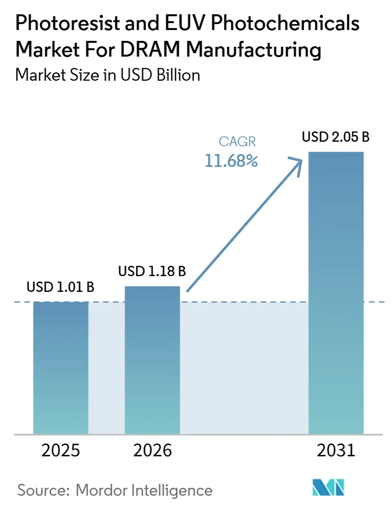
The photoresist and EUV photochemicals market for DRAM manufacturing size is projected to expand from USD 1.01 billion in 2025 and USD 1.18 billion in 2026 to USD 2.05 billion by 2031, registering a CAGR of 11.68% between 2026 and 2031. The growth path reflects a deeper shift in DRAM economics, as each node migration increases patterning intensity per wafer and raises the role of both EUV and ArF immersion materials in production. EUV adoption is no longer limited to a small set of demonstration layers, and the move from two to three EUV layers in earlier generations to at least five layers in SK hynix's 1c architecture has lifted resist consumption per wafer pass. The Photoresist and EUV Photochemicals Market for DRAM Manufacturing is also being shaped by supply concentration, because a small group of qualified Japanese suppliers continues to hold the strongest position at the leading edge while spending heavily on new capacity in Japan, South Korea, and Taiwan. At the same time, PFAS-free reformulation, export controls on advanced semiconductor materials, and the need for domestic supply traceability are splitting demand conditions by region and by node. The result is that the Photoresist and EUV Photochemicals Market for DRAM Manufacturing is growing on a healthy demand base, but the pace of commercialization still depends on how quickly new materials clear fab qualification and move into full-volume DRAM production.
Key Report Takeaways
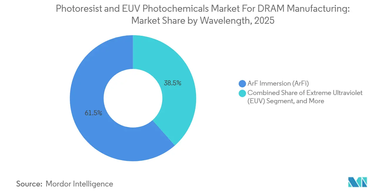
- By wavelength, ArF immersion (ArFi) held 61.54% of the photoresist and EUV photochemicals market for DRAM manufacturing share in 2025, while extreme ultraviolet (EUV) is projected to expand at a 12.67% CAGR through 2031.
- By resist chemistry, chemically amplified resists held 80.12% share in 2025, while metal-oxide resists are projected to grow at a 13.07% CAGR through 2031.
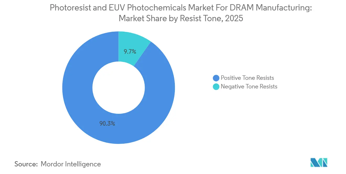
- By resist tone, positive tone resists held 90.28% share in 2025, while negative tone resists are projected to expand at a 12.86% CAGR through 2031.
- By DRAM product type, standard DRAM held 40.38% share in 2025, while High Bandwidth Memory is projected to grow at a 12.83% CAGR through 2031.
- By geography, Asia-Pacific held 88.42% share in 2025, while North America is projected to grow at a 12.56% CAGR through 2031.
Note: Market size and forecast figures in this report are generated using Mordor Intelligence’s proprietary estimation framework, updated with the latest available data and insights as of January 2026.
Market Trends and Insights
Drivers Impact Analysis of Photoresist and EUV Photochemicals Market For DRAM Manufacturing*
| Driver | (~) % Impact on CAGR Forecast | Geographic Relevance | Impact Timeline |
|---|---|---|---|
| Rapid EUV Adoption in Advanced DRAM Patterning | +3.2% | South Korea, Japan, Taiwan, and global demand spill-over | Short term (≤ 2 years) |
| Rising HBM Layer Complexity in AI Servers | +2.5% | South Korea, North America, Europe | Short term (≤ 2 years) |
| Multi-Patterning Demand for ArFi in Mature DRAM Layers | +1.8% | Global, concentrated in South Korea, Japan, and Taiwan | Medium term (2-4 years) |
| Government Fab Incentives for Local Memory Capacity | +1.2% | North America, the EU, and Japan | Medium term (2-4 years) |
| PFAS-Free Reformulation Pull in Semiconductor Materials | +0.8% | EU and Japan, global adoption spillover | Medium term (2-4 years) |
| Dry Resist and Metal-Oxide Throughput Gains | +0.6% | South Korea, Taiwan, North America | Long term (≥ 4 years) |
| Source: Mordor Intelligence | |||
Rapid EUV Adoption in Advanced DRAM Patterning
Rapid EUV adoption has become the strongest growth engine in the photoresist and EUV photochemicals Market for DRAM manufacturing, as advanced DRAM now uses EUV as a recurring production tool rather than a limited process experiment. SK hynix had already expanded EUV use across successive DRAM generations, and its 1c roadmap moved to at least 5 EUV layers per wafer, which raised resist demand in a stepwise manner rather than gradually. The company also installed a TWINSCAN EXE:5200B high-NA EUV system at its Cheongju DRAM fab in September 2025, which pushed material suppliers to prepare for the next qualification cycle earlier than before. In March 2026, SK hynix disclosed a plan to buy more than 30 additional EUV scanners from ASML for KRW 11.95 trillion (USD 8.8 billion), with deliveries scheduled through 2027, and that order volume pointed to a sustained rise in wafer starts requiring qualified resist systems. Once memory customer EUV orders for 2026 were effectively sold out, the bottleneck shifted from tool demand to materials qualification, strengthening the position of suppliers already qualified and raising the near-term entry barrier for new formulations. This shift matters because the photoresist and EUV photochemicals Market for DRAM manufacturing now depends less on whether fabs want EUV and more on whether approved suppliers can scale consistent, production-grade chemistry fast enough to support each added layer.
Rising HBM Layer Complexity In AI Servers
Rising HBM complexity is lifting the quality value of the photoresist and EUV photochemicals Market for DRAM manufacturing, because AI server memory stacks demand tighter lithography control than mainstream DRAM products. HBM4 stack roadmaps are moving to higher layer counts and denser interconnect structures, and that raises sensitivity to overlay, defectivity, and line-edge control across each processing step. That pattern changes supplier economics, because a resist vendor qualified in both advanced logic and advanced memory can spread development costs across larger, high-value accounts while maintaining consistent technical performance across different customer programs. North America also became more relevant when SK hynix secured USD 458 million in CHIPS support for its HBM advanced packaging facility in West Lafayette, Indiana, creating a new premium-grade demand node that will require dependable material support close to its customer base. HBM production also makes yield more valuable, because defect losses carry a larger cost penalty on high-value stacked products than on standard commodity DRAM. As a result, the photoresist and EUV photochemicals market is not only expanding in volume through HBM, it is also moving toward a pricing structure where performance and defect control matter more than simple volume supply.
Multi-Patterning Demand for ArFi in Mature DRAM Layers
Multi-patterning demand for ArFi remains a durable support for the photoresist and EUV photochemicals markets, even as EUV attracts most of the attention around leading-edge DRAM transitions. SPIE conference material on advanced DRAM patterning showed that self-aligned quadruple patterning and crossed SAQP still remain central across several DRAM layers, especially where cost and process control still favor ArFi over full EUV conversion. Each SAQP flow involves several resist-coating, exposure, and development steps, which keep material consumption high even as EUV adoption increases on critical layers. This means ArFi demand is not fading in parallel with each EUV installation, because layer additions in EUV are happening alongside continued multi-patterning in the broader DRAM process flow. Suppliers that already have strong ArFi portfolios therefore retain a stable revenue base while they finance newer EUV and MOR programs. That balance keeps the photoresist and EUV photochemicals Market for DRAM manufacturing broader than a pure EUV story, and it explains why incumbent suppliers continue to invest in both leading-edge and mature lithography chemistries.
Government Fab Incentives for Local Memory Capacity
Government fab incentives have become a structural support for the photoresist and EUV photochemicals market for DRAM manufacturing, because they are creating DRAM production footprints in places that had little or no recent advanced memory manufacturing. In the United States, Micron's Idaho and New York DRAM projects were backed by up to USD 6.4 billion in CHIPS incentives, which marked the return of large-scale leading-edge memory production to the country after a long gap. Samsung also received up to USD 4.745 billion for its Texas operations, further underscoring the need for local material ecosystems that can meet auditability and supply chain traceability requirements. In Japan, policy alignment around semiconductor materials helped support Shin-Etsu Chemical's decision to build a new lithography materials base in Isesaki with Phase 1 investment of JPY 83 billion (USD 557 million), its first new domestic production base in 56 years.[1] These investments matter because they reshape procurement behavior, and fabs receiving policy support increasingly prefer or require domestically qualified or ally-sourced materials. That makes co-location a strategic advantage in the photoresist and EUV photochemicals Market for DRAM manufacturing, not just a logistics preference.
Restraints Impact Analysis of Photoresist and EUV Photochemicals Market For DRAM Manufacturing*
| Restraint | (~) % Impact on CAGR Forecast | Geographic Relevance | Impact Timeline |
|---|---|---|---|
| Long DRAM Fab Qualification Cycles for New Resist Chemistries | -1.5% | Global, most acute in South Korea, Taiwan, Japan | Medium term (2-4 years) |
| EUV Tool Bottlenecks Slowing Material Ramp Rates | -1.2% | Global, concentrated in South Korea, Taiwan | Short term (≤ 2 years) |
| High Purity and Defectivity Requirements Raising Cost of Entry | -0.7% | Global | Long term (≥ 4 years) |
| Export Controls and Raw Material Concentration Risk | -0.6% | China, spill-over to rest of Asia-Pacific | Medium term (2-4 years) |
| Source: Mordor Intelligence | |||
Long DRAM Fab Qualification Cycles For New Resist Chemistries
Long qualification cycles remain the most serious internal restraint on the photoresist and EUV photochemicals market for DRAM manufacturing, because technically promising materials still need extended on-wafer validation before any volume rollout. The problem is especially visible for newer chemistries such as MOR and PFAS-free CAR, where even a favorable lab result does not guarantee a fast transfer into DRAM mass production. Process integration must be checked across exposure tools, tracks, bake conditions, developers, defect maps, and yield windows, and that raises both time and cost before a supplier can secure stable commercial revenue. The result is a structural advantage for incumbent vendors that already sit inside customer flows, because every formulation change at advanced nodes can trigger additional process checks and internal approval cycles. That slows down share shifts in the photoresist and EUV photochemicals Market for DRAM manufacturing and keeps novel entrants from converting technical progress into commercial sales as quickly as demand conditions might suggest. It also explains why capital-backed incumbents are still better positioned than challengers to absorb pre-revenue development costs over multiple DRAM generations.
EUV Tool Bottlenecks Slowing Material Ramp Rates
EUV tool bottlenecks continue to slow the pace at which the photoresist and EUV photochemicals market for DRAM manufacturing can convert demand into actual material shipments. When memory customer EUV tool slots for 2026 were already committed, any installation delay or schedule change directly pushed out the timing of resist consumption on qualified wafers. That bottleneck becomes more severe because materials qualification cannot be completed at full production relevance without access to the same scanner environment planned for volume manufacturing. The pressure is even tighter in high-NA EUV, where the installed base is very small and wafer access for advanced materials programs remains scarce. This means a supplier may have a promising MOR or next-generation EUV formulation but still lack enough production-relevant data to clear customer qualification in time. For the photoresist and EUV photochemicals Market for DRAM manufacturing, a delay loop forms in which tool capacity and material readiness constrain each other rather than advancing at the same pace.
*Our forecasts treat driver/restraint impacts as directional, not additive. The impact forecasts reflect baseline growth, mix effects, and variable interactions.
Photoresist and EUV Photochemicals Market For DRAM Manufacturing Segment Analysis
By Wavelength:
ArFi Anchors Scale While EUV Drives the Next Growth PhaseArF immersion accounted for 61.54% of the photoresist and EUV photochemicals market for DRAM manufacturing in 2025, reflecting its role in repeated patterning flows that still dominate broad sections of the wafer process. The reason is practical, because DRAM makers still rely on SAQP and related multi-patterning methods across several layers, where ArFi remains cost-effective and operationally familiar. That installed base keeps ArFi volume resilient even as more critical layers shift toward EUV, and it prevents a rapid collapse in legacy high-volume resist demand. In the photoresist and EUV photochemicals industry, this creates a dual-track supply need where fabs continue buying large ArFi volumes while also increasing their dependence on qualified EUV materials. Suppliers with broad portfolios, therefore, remain better placed than narrow specialists, because they can support current production while qualifying future layers in parallel.
EUV was the fastest-growing wavelength segment, with a 12.67% CAGR through 2031, reflecting a steady increase in EUV layer counts across advanced DRAM roadmaps. Samsung and SK hynix had already built a meaningful high-NA EUV process base by early 2026, which gave resist vendors a clearer platform for next-step qualification and process tuning. JSR and Inpria also documented progress on both positive-tone and negative-tone MOR systems for low-NA and high-NA EUV applications, which shows that materials development is now moving alongside scanner preparation rather than trailing it. The practical effect is that EUV growth in the photoresist and EUV photochemicals Market for DRAM manufacturing is coming from layer additions rather than simple replacement of ArFi use across the whole wafer. That keeps total material intensity per wafer moving upward, because DRAM nodes are adding new EUV opportunities while still holding on to several ArFi-intensive layers for cost and process reasons in the photoresist and EUV photochemicals market for DRAM manufacturing.

By Resist Chemistry:
CAR Retains Scale While MOR Builds a Faster Technical CaseChemically amplified resists accounted for 80.12% of the photoresist and EUV photochemicals market in 2025, underscoring their deep integration with established track systems, anti-reflective layers, and developer chemistry already used in DRAM fabs. That installed position is difficult to displace because switching the resist chemistry does not affect only the coating bottle; it also affects the surrounding process stack and the customer qualification burden. Sumitomo Chemical and DuPont have continued to advance CAR development for advanced lithography, and DuPont's Qnity team presented work on PFAS alternatives for ArF resist at SPIE in 2025, demonstrating that incumbent chemistry families are still evolving rather than standing still. This matters for the photoresist and EUV photochemicals market because CAR remains the volume foundation that funds the transition into newer chemistry platforms. It also means customers are likely to adopt cleaner or more compliant CAR formulations first across many layers before shifting larger shares of flow to less-proven material classes.
Metal-oxide resists were the fastest-growing chemistry segment, of the photoresist and EUV photochemicals market for DRAM manufacturing, at a 13.07% CAGR over 2026-2031, driven by their stronger EUV photon absorption and their improving throughput profile. Imec showed in February 2026 that an oxygen-enriched post-exposure bake environment improved MOR photo-speed by 15-20%, which directly reduced dose needs and improved scanner productivity under EUV conditions. That result mattered because throughput has been one of the main barriers to wider MOR use, and any dose reduction makes the material case stronger at expensive advanced nodes. JSR's May 2026 cross-licensing agreement with Entegris also showed that MOR competition is moving beyond chemistry alone and into precursor synthesis, filtration, and clean delivery infrastructure.[2] IBM research presented through SPIE 2025 added further support by showing hardware-assisted MOR patterning progress at fine pitches relevant to advanced manufacturing needs. In the photoresist and EUV photochemicals market, MOR is still smaller than CAR today, but its momentum is now tied to measurable process gains rather than to only theoretical promise.
By Resist Tone:
Positive Tone Keeps the Installed Base While Negative Tone Gains on Critical LayersPositive tone resists held 90.28% of the photoresist and EUV photochemicals market share in 2025, supported by their long qualification history in line-space and contact-hole structures used in active areas, bit-lines, and word-lines. Their position also remained strong because process engineers already know how these materials behave within existing integration windows, which lowers operational risk in high-volume manufacturing. Fujifilm extended that position by continuing work on PFAS-free positive-tone and negative-tone ArF immersion systems, and the company presented updated results from its advanced lithography research at SPIE 2026. That matters because regulatory pressure is now reaching mainstream resist families, and suppliers that adapt positive-tone portfolios without disrupting fab performance will defend large installed positions. For the photoresist and EUV photochemicals market, positive tone still sets the volume base, even though the center of innovation is widening beyond traditional wet resist formulations.
Negative tone resists were projected to grow at a 12.86% CAGR through 2031, largely because MOR platforms are increasingly associated with negative-tone behavior on critical EUV layers. Inpria and JSR have continued to advance MOR platforms for both low-NA and high-NA EUV, and those programs highlight why negative-tone materials are becoming more relevant where edge acuity and pattern fidelity are harder to maintain. The appeal is strongest on critical layers where a small improvement in pattern quality can protect a much more expensive wafer process later in the line. Lam Research also widened the competitive picture when its Aether dry photoresist platform was selected in January 2025 by a leading memory manufacturer for advanced DRAM production, because vapor-phase resist deposition challenges older boundaries around tone and wet processing. In the photoresist and EUV photochemicals industry, this means negative-tone growth is not just a small niche expansion, it is part of a broader change in how leading-edge resist performance is being defined. That shift should keep negative-tone and adjacent dry-process platforms more visible in qualification pipelines over the rest of the forecast period in the photoresist and EUV photochemicals market for DRAM manufacturing industry.
By DRAM Product Type:
Standard DRAM Holds The Base While HBM Changes Value CreationStandard DRAM accounted for 40.38% of the photoresist and EUV photochemicals market share in 2025, indicating that mainstream server and client memory still set the baseline for broad material demand. That installed base remains important because resist vendors need dependable, high-volume business to support long development cycles and the expensive customer qualifications required at leading-edge nodes. Standard DRAM also uses a wide mix of mature and advanced lithography layers, giving suppliers room to sell both ArFi-heavy products and newer EUV-qualified materials within a single customer relationship. Specialty and automotive DRAM continue to extend demand for older lithography grades where process stability, qualification continuity, and supply reliability matter more than the most aggressive scaling targets. This broad base keeps the photoresist and EUV photochemicals market from becoming overly dependent on a narrow set of premium products, even as value shifts toward more advanced memory formats.
HBM was the fastest-growing DRAM product type at a 12.83% CAGR over 2026-2031, and that pace reflected the continued rise of AI accelerator demand. Conference material on HBM architecture showed how taller memory stacks and denser interconnect structures raise patterning difficulty and tighten the penalty for defects across each die layer. That changes supplier economics, because premium memory products can justify tighter defect standards and more expensive resist systems if they support stronger yield and throughput. HBM also tends to pull memory production toward the same performance expectations seen in advanced logic, which benefits suppliers that already operate at the top end of lithography qualification. This is why the photoresist and EUV photochemicals market is seeing a clear divide between high-volume standard DRAM demand and high-value HBM demand, even when both sit inside the same customer account. Over time, HBM should keep increasing the share of demand tied to top-tier resist quality, especially as AI server deployments continue to scale across global cloud and accelerator programs.
Geography Analysis
APAC Photoresist and EUV Photochemicals Market for DRAM Manufacturing
Asia-Pacific accounted for 88.42% of the photoresist and EUV photochemicals market in 2025, making the region the clear center of both consumption and supply. South Korea remained the largest national demand base because Samsung Electronics and SK Hynix continued to anchor advanced DRAM output and forward EUV investment. SK hynix strengthened that outlook in March 2026 when it disclosed its KRW 11.95 trillion (USD 8.8 billion) EUV scanner purchase plan through 2027, which supported a longer visible demand pipeline for qualified materials. Japan remained just as important on the supply side, as TOK, JSR, Shin-Etsu Chemical, Sumitomo Chemical, and Fujifilm continued to operate dense R&D and production networks for semiconductor materials, including new domestic investment from Shin-Etsu in Isesaki.
North America Photoresist and EUV Photochemicals Market for DRAM Manufacturing
North America was the fastest-growing geography, with a 12.56% CAGR over 2026-2031, reflecting a new phase of DRAM manufacturing investment rather than a typical capacity refresh cycle. Micron's Idaho and New York projects, backed by up to USD 6.4 billion in CHIPS support, created the strongest long-term case for domestic memory materials demand in the region. SK hynix also added a premium demand point through its USD 458 million supported HBM packaging project in Indiana, while Samsung's Texas investment widened the broader semiconductor materials opportunity across the United States. This new build-out matters because the photoresist and EUV photochemicals market in North America is being shaped by domestic qualification, PFAS scrutiny, and supply chain traceability requirements more than by legacy installed capacity.
Europe Photoresist and EUV Photochemicals Market for DRAM Manufacturing
Europe held a modest share, but it remained strategically important because much of the region's influence came through process development rather than through direct DRAM wafer volume. Imec's NanoIC and EUV research programs in Belgium continued to support resist co-development, and the institute's February 2026 MOR work showed a 15-20% photo-speed improvement under oxygen-enriched post-exposure bake conditions.[3] That gave Europe an outsized role in advancing next-generation lithography readiness even without a comparable share of global DRAM output. The Rest of the World remained negligible for current DRAM photoresist demand, because emerging fab plans outside the main clusters have not yet reached the scale needed to materially change near-term purchasing patterns in the photoresist and EUV photochemicals market for DRAM manufacturing.
Competitive Landscape
The phphotoresist and EUV photochemicals market for DRAM manufacturing remained highly concentrated at the leading edge, because commercial DRAM qualification still favored a small group of suppliers with long customer histories, deep process integration, and the capital needed for repeated node transitions. Tokyo Ohka Kogyo, JSR Corporation, and Shin-Etsu Chemical continued to hold the strongest structural positions in advanced DRAM photoresist supply, while Fujifilm and Sumitomo Chemical remained important across adjacent lithography and formulation categories. This concentration was reinforced by capacity spending rather than by pricing alone, as leading suppliers continued to build new plants near customer fabs in Japan, South Korea, and Taiwan. TOK announced the construction of a new Pyeongtaek plant in South Korea, with a Phase 1 investment of JPY 12 billion (USD 80.5 million). The site is scheduled to support Samsung and SK hynix's process needs from the second half of 2027.[4] Shin-Etsu Chemical also moved ahead with its Isesaki base in Japan, investing JPY 83 billion (USD 557 million) in Phase 1, demonstrating that leading suppliers were using domestic manufacturing depth as a competitive moat.
A second layer of competition has been forming around platform integration, where the supplier that controls chemistry, precursor quality, filtration, and process support can gain an advantage that is harder to copy. Entegris and JSR or Inpria moved in that direction in May 2026 through a non-exclusive MOR cross-licensing agreement that joined material innovation with clean delivery infrastructure. Fujifilm pursued another path by moving early on PFAS-free resist development, first in negative-type ArF immersion materials and then toward broader advanced lithography extensions. Lam Research remained a different kind of competitor, because its Aether dry photoresist platform challenged the wet chemistry model itself by moving resist application into a vapor-phase production approach. These moves show that competition in the photoresist and EUV photochemicals market is no longer limited to who makes a better bottle of resist, it now includes who controls the wider process platform.
The photoresist and EUV photochemicals market for DRAM manufacturing industry also remained difficult for smaller challengers, because technical progress alone was not enough to win business at Tier-1 DRAM fabs. Long qualification cycles, customer-specific process windows, and the cost of clean manufacturing all continued to favor incumbents with established balance sheets and on-site support capabilities. At the same time, white-space opportunities still existed in PFAS-free EUV chemistry, MOR systems tuned for high-NA EUV, and local supply qualification in North America where new fabs are creating fresh procurement needs. That is why the photoresist and EUV photochemicals market looked concentrated today, but not closed, because partnerships, cross-licensing, and region-specific supply moves were still changing the shape of competition beneath the top tier.
Leaders of Photoresist and EUV Photochemicals Market For DRAM Manufacturing
-
Tokyo Ohka Kogyo Co., Ltd.
-
JSR Corporation
-
Shin-Etsu Chemical Co., Ltd.
-
FUJIFILM Holdings Corporation
-
Sumitomo Chemical Co., Ltd.
- *Disclaimer: Major Players sorted in no particular order
Photoresist and EUV Photochemicals Market For DRAM Manufacturing Companies Covered in this Report
- Tokyo Ohka Kogyo Co., Ltd.
- JSR Corporation
- Shin-Etsu Chemical Co., Ltd.
- FUJIFILM Holdings Corporation
- Sumitomo Chemical Co., Ltd.
- DuPont de Nemours, Inc.
- Merck KGaA
- Dongjin Semichem Co., Ltd.
- Brewer Science, Inc.
- Inpria Corporation
- Lam Research Corporation
- Allresist GmbH
- micro resist technology GmbH
- Microchemicals GmbH
- Eternal Materials Co., Ltd.
- Jiangsu Nata Opto-electronic Material Co., Ltd.
- Hubei Dinglong Co., Ltd.
- S&S Tech Corporation
Recent Industry Developments in Photoresist and EUV Photochemicals Market For DRAM Manufacturing
- May 2026: Entegris, Inc. and JSR Corporation/Inpria Corporation announced a non-exclusive cross-licensing agreement for metal-oxide resist patents, terminating the Inter Partes Review challenge. The agreement encompasses collaborative development in resist formulation, CVD/ALD precursor synthesis, and MOR-specific filtration, effectively integrating two critical nodes of the EUV materials supply chain into a joint innovation pathway.
- May 2026: JSR Corporation announced plans to build its first Taiwan photoresist production facility, intended to co-develop advanced resists with TSMC and close a proximity gap relative to TOK and Shin-Etsu Chemical, both of which already operate Taiwan-based production. The facility is expected to be operational as early as 2028 and may also produce other semiconductor materials, including polishing abrasives.
- April 2026: FUJIFILM Corporation announced the world's first fluorine-free negative ArF immersion photoresist and began distributing samples to customers for evaluation toward early commercialization. The product targets advanced nodes used in AI semiconductor manufacturing, and Fujifilm intends to extend fluorine-free chemistry to EUV photoresists as a follow-on development.
- March 2026: SK hynix disclosed a regulatory filing to purchase over 30 EUV scanners from ASML for KRW 11.95 trillion (USD 8.8 billion), with delivery scheduled through December 2027. The systems will be deployed at Icheon, Cheongju, and Yongin fabs to support 1c DRAM and HBM4E production ramps.
Scope of Report on Photoresist and EUV Photochemicals Market For DRAM Manufacturing
The photoresist and EUV photochemicals market for DRAM manufacturing industry covers the materials used in photolithography processes to pattern semiconductor wafers for dynamic random-access memory production, including photoresists, EUV resists, developers, anti-reflective coatings, and related process chemicals used across advanced DRAM fabrication nodes.
The Photoresist and EUV Photochemicals Market for DRAM Manufacturing Industry Report is Segmented by Wavelength (Extreme Ultraviolet [EUV], ArF Immersion [ArFi], KrF, and I-Line/G-Line), Resist Chemistry (Chemically Amplified Resists [CAR], Metal-Oxide Resists [MOR], and Non-CAR Organic Resists), Resist Tone (Positive Tone Resists, and Negative Tone Resists), DRAM Product Type (Standard DRAM, Mobile DRAM [LPDDR], Graphics DRAM [GDDR], High Bandwidth Memory [HBM], Server DRAM, and Other DRAM Product Types), and Geography (North America, Europe, Asia-Pacific, and Rest of the World). The Market Forecasts are Provided in Terms of Value (USD).
Segmentation Overview
| Extreme Ultraviolet (EUV) |
| ArF Immersion (ArFi) |
| KrF |
| I-Line/G-Line |
| Chemically Amplified Resists (CAR) |
| Metal-Oxide Resists (MOR) |
| Non-CAR Organic Resists |
| Positive Tone Resists |
| Negative Tone Resists |
| Standard DRAM |
| Mobile DRAM (LPDDR) |
| Graphics DRAM (GDDR) |
| High Bandwidth Memory (HBM) |
| Server DRAM |
| Other DRAM Product Types |
| North America | |
| Europe | |
| Asia-Pacific | China |
| Japan | |
| South Korea | |
| Taiwan | |
| Rest of Asia-Pacific | |
| Rest of the World |
| By Wavelength | Extreme Ultraviolet (EUV) | |
| ArF Immersion (ArFi) | ||
| KrF | ||
| I-Line/G-Line | ||
| By Resist Chemistry | Chemically Amplified Resists (CAR) | |
| Metal-Oxide Resists (MOR) | ||
| Non-CAR Organic Resists | ||
| By Resist Tone | Positive Tone Resists | |
| Negative Tone Resists | ||
| By DRAM Product Type | Standard DRAM | |
| Mobile DRAM (LPDDR) | ||
| Graphics DRAM (GDDR) | ||
| High Bandwidth Memory (HBM) | ||
| Server DRAM | ||
| Other DRAM Product Types | ||
| By Geography | North America | |
| Europe | ||
| Asia-Pacific | China | |
| Japan | ||
| South Korea | ||
| Taiwan | ||
| Rest of Asia-Pacific | ||
| Rest of the World | ||
Key Questions Answered in the Report
What is the size outlook for the photoresist and EUV photochemicals market for DRAM manufacturing?
The photoresist and EUV photochemicals market for DRAM manufacturing was valued at USD 1.01 billion in 2025, reached USD 1.18 billion in 2026, and is projected to reach USD 2.05 billion by 2031 at an 11.68% CAGR.
Which wavelength segment leads DRAM photoresist demand today?
ArF immersion led with 61.54% share in 2025 because most DRAM layers still rely on repeated multi-patterning flows, even as EUV adoption rises on critical layers.
Why does EUV resist demand increasing so quickly in DRAM production?
EUV layer counts are increasing across advanced DRAM nodes, and this raises resist consumption per wafer while strengthening demand for already qualified suppliers and advanced chemistries.
How is HBM changing material requirements in memory fabrication?
HBM is the fastest-growing DRAM product type at 12.83% CAGR, and its tighter yield and defect standards are increasing demand for premium-grade lithography materials.
Which region is growing fastest for new DRAM photoresist demand?
North America is projected to grow at a 12.56% CAGR through 2031, supported by CHIPS-funded fab construction and the need for domestic or proximate qualified materials.
What is the main barrier for new resist chemistries entering advanced DRAM fabs?
The biggest challenge is the long qualification cycle, because new materials must prove stable performance across scanner settings, process windows, and yield targets before full deployment.