Semiconductor Lithography Equipment Market Size and Share
Market Overview
| Study Period | 2020 - 2031 |
|---|---|
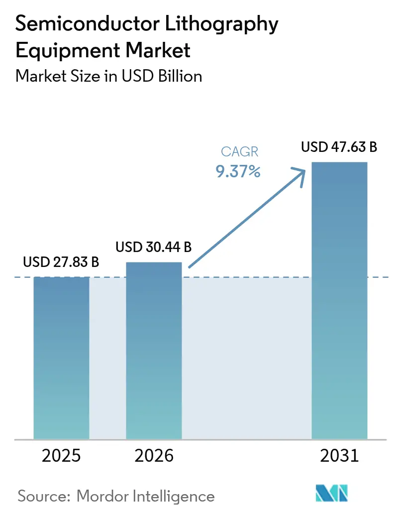
| Market Size (2026) | USD 30.44 Billion |
| Market Size (2031) | USD 47.63 Billion |
| Growth Rate (2026 - 2031) | 9.37% CAGR |
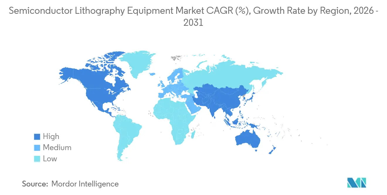
| Fastest Growing Market | North America |
| Largest Market | Asia Pacific |
| Market Concentration | High |
Major Players*Disclaimer: Major Players sorted in no particular order Image © Mordor Intelligence. Reuse requires attribution under CC BY 4.0. | |
Semiconductor Lithography Equipment Market Analysis by Mordor Intelligence
The semiconductor lithography equipment market size is projected to expand from USD 27.83 billion in 2025 and USD 30.44 billion in 2026 to USD 47.63 billion by 2031, registering a CAGR of 9.37% between 2026-2031. Rising allocations toward extreme ultraviolet (EUV) and high-numerical-aperture (High-NA) scanners, sustained demand for deep ultraviolet (DUV) tools at 28-180 nanometer nodes, and large-scale regional subsidy programs are together reshaping capital-spending priorities. Device makers are front-loading orders for High-NA platforms that shorten process flows to a single exposure, even as DUV immersion scanners preserve cost leadership for power and automotive chips. Equipment lifecycles are compressing as logic foundries race to introduce 2-nanometer and 1.4-nanometer nodes before 2029, redirecting vendor roadmaps toward service-driven revenue, adaptive optics, and closed-loop metrology. Geopolitical bifurcation is fragmenting customer portfolios, forcing suppliers to balance compliance risk with growth in China-restricted regions. At the same time, advanced-packaging investments are spawning a parallel tool segment that values throughput and large-panel formats over absolute resolution, broadening addressable demand beyond front-end fabs.
Key Report Takeaways
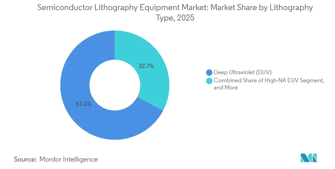
- By lithography type, deep ultraviolet lithography led with 67.31% of the semiconductor lithography equipment market share in 2025, while High-NA EUV is projected to advance at a 10.12% CAGR through 2031.
- By application, advanced packaging captured 36.74% of 2025 revenue, and research and development prototyping is forecast to expand at a 10.39% CAGR over 2026-2031.
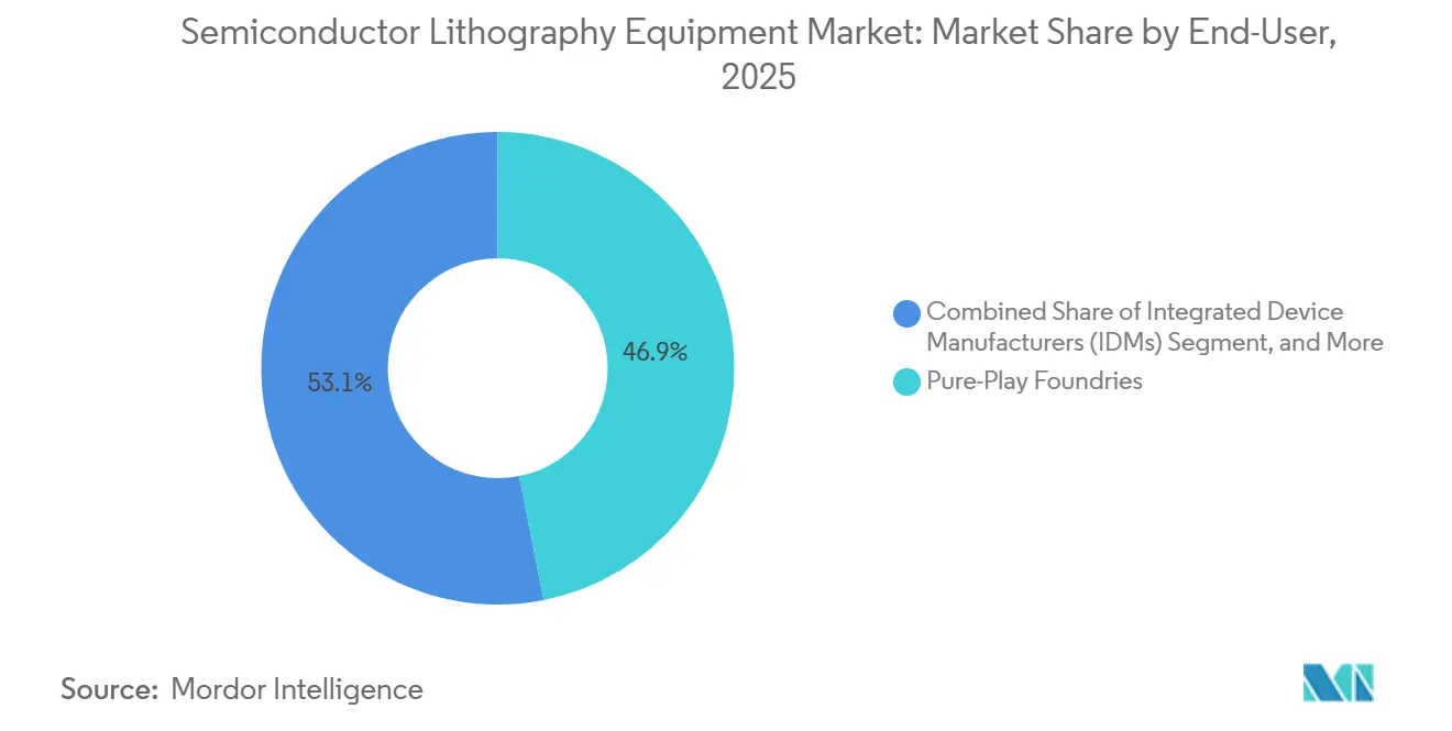
- By end-user, pure-play foundries accounted for 46.89% of the semiconductor lithography equipment market share in 2025, whereas outsourced semiconductor assembly and test providers are expected to register the fastest growth at a 9.96% CAGR during the forecast period.
- By wafer size, 300 millimeter substrates dominated with 72.67% of the semiconductor lithography equipment market share in 2025, while the emerging 450 millimeter segment is anticipated to grow at a 9.91% CAGR to 2031.
- By geography, Asia-Pacific accounted for 63.58% of 2025 revenue, and North America is set to post the fastest regional pace with a 10.33% CAGR through 2031.
Note: Market size and forecast figures in this report are generated using Mordor Intelligence’s proprietary estimation framework, updated with the latest available data and insights as of 2026.
Global Semiconductor Lithography Equipment Market Trends and Insights
Drivers Impact Analysis*
| Driver | (~) % Impact on CAGR Forecast | Geographic Relevance | Impact Timeline |
|---|---|---|---|
| Shrinking Process Nodes Driving EUV Adoption | +2.6% | Global, concentrated in Taiwan, South Korea, United States | Medium term (2-4 years) |
| Surging AI and Data Center Demand for Advanced Logic Chips | +2.3% | Global, led by North America and Asia-Pacific | Short term (≤ 2 years) |
| Government Fab Subsidies such as CHIPS and EU Chips Acts | +1.7% | North America and Europe, spillover to Asia-Pacific partnerships | Medium term (2-4 years) |
| Expansion of 3D Heterogeneous Integration and Advanced Packaging | +1.4% | Asia-Pacific core, expanding to North America and Europe | Long term (≥ 4 years) |
| Metal Oxide Photoresists Reducing Stochastic Defects Below 2 nm | +0.5% | Global, early adoption in Taiwan and United States | Long term (≥ 4 years) |
| EUV Pellicle Commercialization Shortening Tool Downtime | +0.3% | Global, concentrated in leading-edge fabs | Short term (≤ 2 years) |
| Source: Mordor Intelligence | |||
Shrinking Process Nodes Driving EUV Adoption
Multi-patterning with DUV immersion scanners now fails internal cost targets once half-pitch features drop below 16 nanometers. Intel validated single-exposure High-NA throughput of 175-220 wafers per hour for its 18A process, eliminating quadruple-patterning overlay losses.[1]Intel Corporation, “Intel Completes High-NA EUV Acceptance Testing,” INTEL.COM Samsung secured High-NA slots in late 2025 to accelerate its 2-nanometer gate-all-around roadmap. TSMC, by contrast, is stretching 0.33 NA EUV with hybrid pellicles and advanced resist chemistries that safeguard its installed base. This phased adoption concentrates pricing power in ASML, whose EUV backlog reached EUR 38.8 billion at year-end 2025.
Surging AI and Data Center Demand for Advanced Logic Chips
Generative-AI accelerators require up to 3× as many lithography steps as traditional CPUs, expanding logic-foundry tool budgets. Deloitte projects AI-chip revenue of roughly USD 500 billion in 2026, or half of total semiconductor sales. TSMC plans to quadruple CoWoS substrate capacity to 130,000 wafers per month, with each line requiring sub-1-micrometer overlay on 600 × 600 millimeter panels. OSATs are adding advanced steppers to support through-silicon-via (TSV) stacking for HBM3E devices, whose 16-layer stacks increase lithography intensity. The interplay of EUV compute tiles with DUV I/O dies sustains parallel demand across equipment generations.
Government Fab Subsidies such as CHIPS and the EU Chips Acts
The CHIPS and Science Act assigned approximately USD 34 billion to 40 projects by late 2025, lowering equity hurdles for eight leading-edge fabs and dozens of supply-chain plants. Europe’s Chips Act steers EUR 43 billion (USD 45.9 billion) into incentives, including more than EUR 5 billion for a Dresden joint venture between TSMC, Bosch, Infineon, and NXP.[2]European Commission, “European Chips Act: Commission Approves EUR 5 Billion German Aid,” EUROPA.EU Japan earmarked JPY 2.9 trillion (USD 18.1 billion) to bankroll Rapidus and lure High-NA allocations. Subsidy tranches unlock only when construction milestones are met, aligning tool deliveries with domestic-content goals.
Expansion of 3D Heterogeneous Integration and Advanced Packaging
Advanced-packaging fabs are migrating from 300-millimeter wafers to 600 × 600 millimeter panels that triple-die-image per exposure. Applied Materials’ PLP2 direct-laser tool patterns sub-1 micrometer redistribution layers on full-size panels, cutting cycle time by 25% versus reticle-based exposure.[3]Applied Materials, “Applied Materials Introduces PLP2 for Advanced Packaging,” APPLIEDMATERIALS.COM Onto Innovation’s JetStep X500 addresses mid-tier panel geometries where cost per square millimeter dominates. EV Group’s maskless platform eliminates photomask expenses for rapid-turn fan-out prototypes. The shift draws OSATs into direct competition with logic foundries for lithography capital.
Restraints Impact Analysis*
| Restraint | (~) % Impact on CAGR Forecast | Geographic Relevance | Impact Timeline |
|---|---|---|---|
| Export-Control Restrictions to China | -1.8% | Asia-Pacific, concentrated in China | Short term (≤ 2 years) |
| Ultra-High Capex of EUV Scanners | -1.2% | Global, acute in emerging fab regions | Medium term (2-4 years) |
| Helium Supply Volatility Raising Operating Costs | -0.5% | Global, most acute where recycling is limited | Short term (≤ 2 years) |
| Cleanroom Carbon Footprint Limits from ESG Mandates | -0.3% | Europe and North America, emerging in Asia-Pacific | Long term (≥ 4 years) |
| Source: Mordor Intelligence | |||
Export-Control Restrictions to China
Dutch rules enacted in 2024 block ASML’s NXT:2050i and NXT:2100i immersion systems from unlicensed shipment to China, trimming ASML’s regional revenue share from 33% in 2024 to 20% in 2026. Japan mirrored limits on Nikon and Canon DUV tools, while Washington studies service-ban scenarios. SMIC’s 7-nanometer output, achieved via DUV multi-patterning, trails TSMC yields by up to 30 percentage points and is viable only for low-margin niches. Domestic subsidies channel orders to Shanghai Micro Electronics Equipment, yet gaps in lens coatings and stage metrology suggest a five-year lag behind Western peers.
Ultra-High Capex of EUV Scanners
High-NA scanners list above USD 400 million per unit, equivalent to eight DUV immersion tools, and require annual service contracts of USD 15-25 million. Smaller semiconductor fabrication plants (fabs) are strategically extending the lifecycle of their 7-nanometer nodes by implementing design-rule modifications, rather than transitioning to the more advanced 3-nanometer nodes. This approach has effectively placed a limitation on unit demand within the market. Furthermore, the requirement for deposits to be made 12-18 months prior to delivery has significantly heightened the strain on working capital, particularly during periods of macroeconomic uncertainty.
*Our forecasts treat driver/restraint impacts as directional, not additive. The impact forecasts reflect baseline growth, mix effects, and variable interactions.
Segment Analysis
By Lithography Type: Dual Demand for EUV and DUV Shapes Spending
Deep ultraviolet systems generated 67.31% of the semiconductor lithography equipment market share in 2025, reflecting continued demand from power, analog, and automotive devices that run on mature-node flows. Extreme ultraviolet platforms, particularly High-NA tools, are projected to post a 10.12% CAGR during 2026-2031 as leading-edge fabs target single-exposure patterning at 2 nanometers and below. Intel validated 0.55 NA throughput of 175-220 wafers per hour on its first High-NA scanner in January 2026, proving that overlay-error accumulation can be eliminated without costly multi-patterning. TSMC is stretching 0.33 NA EUV with hybrid pellicles and computational lithography to preserve capital efficiency until 2027-2028, illustrating how customer roadmaps dictate tool-mix pacing.
Maskless digital lithography remains confined to prototyping and advanced packaging, where EV Group’s LITHOSCALE XT achieves sub-2-micrometer resolution on 300-millimeter wafers. DUV immersion scanners will therefore coexist with EUV throughout the forecast, as 28-180 nanometer nodes still account for half of global wafer starts. Vendors are layering adaptive optics and service analytics onto installed DUV bases, converting legacy fleets into recurring revenue engines. The resulting dual-track spending keeps the semiconductor lithography equipment market size diversified across both high-resolution and cost-optimized platforms.


By Application: Packaging Upswing Redefines Tool Mix
Advanced packaging captured 36.74% of the semiconductor lithography equipment market size in 2025, propelled by chiplet integration and fan-out wafer-level processing that require <2 micrometer overlay across heterogeneous die stacks. High-bandwidth-memory assemblies drive multiple redistribution-layer exposures, thereby amplifying the number of stepper cycles per unit substrate. Research and development prototyping shows the fastest trajectory at a 10.39% CAGR, as iwithc’s 300-millimeter gallium line and Rapidus’s 2-nanometer line require 2-nanometer multi-configuration exposure stages. TSMC, meanwhile, is quadrupling CoWoS capacity to 130,000 wafers per month, spurring fresh panel-level orders for 600 × 600 millimeter substrates.
MEMS sensors and LED producers seek mid-resolution scanners that balance price with moderate overlay, sustaining DUV sales even as EUV dominates logic. Power and compound-semiconductor makers demand tools that are tolerant of thick GaN and SiC wafers, prompting Veeco to launch the Propel300 in November 2025 for automotive power modules. As toolmakers tailor optics for diverse substrates, the semiconductor lithography equipment market share fragments along application-specific performance lines. Hybrid lines that couple EUV front-end patterning with panel-level packaging exposure emerge as the mainstream configuration for AI accelerators and premium mobile chipsets.
By End-User: Foundry Leadership Faces OSAT Acceleration
Pure-play foundries accounted for 46.89% of spending in 2025, underpinned by TSMC’s USD 52-56 billion capital budget and Samsung’s early High-NA allocations. Outsourced semiconductor assembly and test providers are forecast to grow at a 9.96% CAGR through 2031, the fastest end-user pace, as chiplet architectures redirect lithography intensity toward redistribution-layer patterning and interposer fabrication. SJ Semiconductor’s USD 700 million fundraise for 2.5D and 3D packaging exemplifies OSAT's ambitions to run lithography lines comparable to those of logic fabs. This downstream surge expands the customer base for large-panel tools and erodes the historical dominance of front-end fabs.
Integrated device manufacturers now split into two camps: Intel and Samsung add EUV capacity to regain process leadership, while analog specialists such as Texas Instruments extend 110-nanometer nodes with incremental design rules. ACM Research’s February 2026 sales of 310 × 310- and 600 × 600-millimeter panel-stepper systems confirm OSAT interest in large-area exposure. As foundries, IDMs, and OSATs converge on overlapping lithography needs, equipment suppliers must customize optics, automation, and service bundles for a broader operational spectrum, preserving growth momentum across the semiconductor lithography equipment market.
By Wafer Size: 300 mm Entrenchment vs. 450 mm Trials
The 300-millimeter format accounted for 72.67% of the semiconductor lithography equipment market share in 2025, reflecting entrenched fab investments and supply-chain standardization. Most leading-edge EUV installations and all panel-level advanced-packaging lines currently rely on 300 millimeter wafer logistics. Prototype 450-millimeter activities are projected to grow at a 9.91% CAGR over 2026-2031, but these efforts remain limited to research consortia because high-volume economics are unproven and EUV compatibility remains unresolved. Tool vendors therefore downprioritize 450-millimeter optics in favor of software and metrology upgrades for existing fleets.
Meanwhile, 600 × 600 millimeter panel-level substrates in advanced packaging outpace wafer-scale scaling by offering triple-die yield per exposure without retooling front-end cleanrooms. Veeco’s USD 35 million order book for 200 millimeter steppers in May 2025 demonstrates ongoing demand for niche formats in MEMS, SiC, and GaN lines. The semiconductor lithography equipment market thus remains anchored to 300-millimeter wafers while expanding sideways into large-area panels, underscoring that heterogeneous integration, not larger wafers, holds the next cost-reduction frontier.
Geography Analysis
Asia-Pacific accounted for 63.58% of 2025 revenue, keeping the region at the center of the semiconductor lithography equipment market. Taiwan anchors this lead through TSMC’s high-volume EUV factories, while South Korea accelerates High-NA deployments to narrow yield gaps with TSMC at the 2-nanometer node. Japan’s JPY 2.9 trillion Rapidus program schedules 2-nanometer production in 2026, with imec support and pre-allocated High-NA scanners. India’s USD 11 billion Tata-PSMC joint venture targets 28-110 nanometer automotive and industrial chips, adding mature-node lithography demand in South Asia. China faces reduced tool inflows after Dutch export controls, yet domestic subsidies expand Shanghai Micro Electronics Equipment’s installed base inside legacy fabs.
North America is forecast to record the fastest regional growth, advancing at a 10.33% CAGR through 2031, as CHIPS Act incentives de-risk eight leading-edge fabs and dozens of supply-chain projects. TSMC’s Arizona complex has expanded to six fabs and two advanced-packaging plants, totaling more than USD 165 billion in planned spending. Intel validated its first High-NA scanner in Oregon in January 2026, confirming domestic access to the newest patterning platform. Micron’s New York DRAM project and Samsung’s Texas logic fab add DUV immersion demand at mature and specialty nodes. Corning’s photomask-blank facility and Edwards’ vacuum-pump expansion localize critical consumables, tightening regional supply loops for the semiconductor lithography equipment market size.
Europe mobilizes EUR 43 billion in public and private funding under the Chips Act, highlighted by the EUR 10 billion Dresden joint venture that will start 28-12 nanometer output in 2027. Intel’s Magdeburg plan, backed by EUR 9.9 billion in German support, awaits 18A yield maturity before full construction ramps. Infineon opened a EUR 5 billion power semiconductor fab in Dresden in 2026, using DUV scanners optimized for silicon carbide devices. The Middle East and Africa, and South America, remain exploratory, with Gulf states evaluating foundry partnerships but no confirmed leading-edge projects. Regional incentives, export-control compliance, and workforce readiness will ultimately dictate how quickly each geography can convert subsidies into sustainable lithography demand.

Competitive Landscape
ASML dominates extreme-ultraviolet systems and holds more than 85% of DUV immersion shipments, backed by a EUR 38.8 billion backlog that locks in multi-year revenue visibility. High-NA roadmaps that aim to reach 0.75 numerical aperture by 2030 require USD 1-2 billion per generation, reinforcing entry barriers that only a near-monopoly can afford. ASML also layers subscription analytics and wafer-stage upgrades onto its installed fleet, turning service into a stable profit engine.
Nikon and Canon retreat to niche segments rather than contest EUV, focusing on cost-sensitive DUV steppers and nanoimprint systems. Canon’s 2025 factory expansion boosts nanoimprint capacity for 5-nanometer patterning, offering a lower-cost alternative to EUV’s USD 200-million price tags that deter buyers. Nikon addresses legacy analog and MEMS markets with mid-resolution scanners that emphasize cycle-time efficiency. White-space innovators such as Onto Innovation, EV Group, and Applied Materials attack advanced-packaging workflows with panel-level tools that bypass masks, patterning 600 × 600 millimeter substrates at sub-1 micrometer overlay.
Chinese vendors focus on mature nodes under domestic-preference mandates. Shanghai Micro Electronics Equipment remains limited to 90-nanometer steppers but expands installations through state procurement budgets. ACM Research captured February 2026 panel-level orders from OSATs, signaling momentum for indigenous large-area exposure platforms. Export controls carve the market into Western-aligned, leading-edge demand and China-centric, legacy demand, forcing global suppliers to diversify their customer mixes. As advanced-packaging spending rises, competition shifts from resolution leadership to total cost of ownership, service responsiveness, and substrate flexibility, preserving growth for challengers while maintaining ASML’s primary hold on the semiconductor lithography equipment market share.
Semiconductor Lithography Equipment Industry Leaders
ASML Holding N.V.
Nikon Corporation
Canon Inc.
SÜSS MicroTec SE
Veeco Instruments Inc.
- *Disclaimer: Major Players sorted in no particular order

Recent Industry Developments
- February 2026: ACM Research received multiple panel-level lithography system orders for 310 × 310 mm, 510 × 515 mm, and 600 × 600 mm formats aimed at redistribution-layer capacity expansion among OSATs.
- February 2026: EV Group introduced the EVG120 resist processing system for 200-300 mm wafers and 600 × 600 mm panels, cutting cycle time by 25% over prior tools.
- January 2026: Intel completed acceptance testing of the first High-NA EUV scanner, the ASML EXE:5200B, validating 0.55 NA throughput for 18A and 14A nodes.
- November 2025: Veeco Instruments launched the Propel300 MOCVD system for 300 mm GaN-on-silicon power devices targeting automotive modules.


Global Semiconductor Lithography Equipment Market Report Scope
The Semiconductor Lithography Equipment Market Report is Segmented by Lithography Type (Deep Ultraviolet (DUV), Extreme Ultraviolet (EUV), High-NA EUV, Maskless Digital Lithography), Application (Advanced Packaging, MEMS Devices, LED Devices, Power and Compound Semiconductors, Research and Development Prototyping), End-User (Pure-Play Foundries, Integrated Device Manufacturers (IDMs), Outsourced Semiconductor Assembly and Test (OSAT)), Wafer Size (200 mm, 300 mm, 450 mm), and Geography (North America, South America, Europe, Asia-Pacific, Middle East and Africa). The Market Forecasts are Provided in Terms of Value (USD).
| Deep Ultraviolet (DUV) |
| Extreme Ultraviolet (EUV) |
| High-NA EUV |
| Maskless Digital Lithography |
| Advanced Packaging |
| MEMS Devices |
| LED Devices |
| Power and Compound Semiconductors |
| Research and Development Prototyping |
| Pure-Play Foundries |
| Integrated Device Manufacturers (IDMs) |
| Outsourced Semiconductor Assembly and Test (OSAT) |
| 200 mm |
| 300 mm |
| 450 mm |
| North America | United States | |
| Canada | ||
| Mexico | ||
| South America | Brazil | |
| Argentina | ||
| Rest of South America | ||
| Europe | United Kingdom | |
| Germany | ||
| France | ||
| Italy | ||
| Rest of Europe | ||
| Asia-Pacific | China | |
| Japan | ||
| India | ||
| South Korea | ||
| Rest of Asia-Pacific | ||
| Middle East and Africa | Middle East | United Arab Emirates |
| Saudi Arabia | ||
| Rest of Middle East | ||
| Africa | South Africa | |
| Egypt | ||
| Rest of Africa | ||
| By Lithography Type | Deep Ultraviolet (DUV) | ||
| Extreme Ultraviolet (EUV) | |||
| High-NA EUV | |||
| Maskless Digital Lithography | |||
| By Application | Advanced Packaging | ||
| MEMS Devices | |||
| LED Devices | |||
| Power and Compound Semiconductors | |||
| Research and Development Prototyping | |||
| By End-User | Pure-Play Foundries | ||
| Integrated Device Manufacturers (IDMs) | |||
| Outsourced Semiconductor Assembly and Test (OSAT) | |||
| By Wafer Size | 200 mm | ||
| 300 mm | |||
| 450 mm | |||
| By Geography | North America | United States | |
| Canada | |||
| Mexico | |||
| South America | Brazil | ||
| Argentina | |||
| Rest of South America | |||
| Europe | United Kingdom | ||
| Germany | |||
| France | |||
| Italy | |||
| Rest of Europe | |||
| Asia-Pacific | China | ||
| Japan | |||
| India | |||
| South Korea | |||
| Rest of Asia-Pacific | |||
| Middle East and Africa | Middle East | United Arab Emirates | |
| Saudi Arabia | |||
| Rest of Middle East | |||
| Africa | South Africa | ||
| Egypt | |||
| Rest of Africa | |||


Key Questions Answered in the Report
How fast is demand for High-NA EUV tools expected to grow?
High-NA EUV equipment revenue is projected to rise at a 10.12% CAGR between 2026-2031 as leading-edge fabs migrate to sub-2 nanometer nodes.
Which region is expanding lithography spending the quickest?
North America shows the fastest regional pace, with a 10.33% CAGR through 2031, driven by CHIPS Act incentives and multiple new fab projects.
Why do OSATs matter to lithography suppliers now?
Chiplet architectures push redistribution-layer patterning downstream, enabling OSATs to invest in panel-level steppers and capture a 9.96% CAGR through 2031.
What keeps 300 mm wafers dominant despite 450 mm pilots?
Legacy fab infrastructure and the pivot toward 600 mm panel-level packaging deliver superior cost scaling without massive 450 mm capital outlays.
How are export controls influencing Chinese lithography demand?
Restrictions on DUV immersion tools cut China’s share of ASML revenue to about 20% in 2026, steering domestic fabs toward mature nodes and indigenous equipment.
Which application segment leads revenue today?
Advanced packaging holds the largest share at 36.74% of 2025 revenue, fueled by chiplet integration and fan-out wafer-level processing requirements.
Page last updated on:


