Chiplet Market Size and Share
Market Overview
| Study Period | 2020 - 2031 |
|---|---|
| Market Size (2026) | USD 65.31 Billion |
| Market Size (2031) | USD 188.79 Billion |
| Growth Rate (2026 - 2031) | 23.65% CAGR |
| Fastest Growing Market | North America |
| Largest Market | Asia-Pacific |
| Market Concentration | Medium |
Major Players *Disclaimer: Major Players sorted in no particular order Image © Mordor Intelligence. Reuse requires attribution under CC BY 4.0. | |
Chiplet Market Analysis by Mordor Intelligence
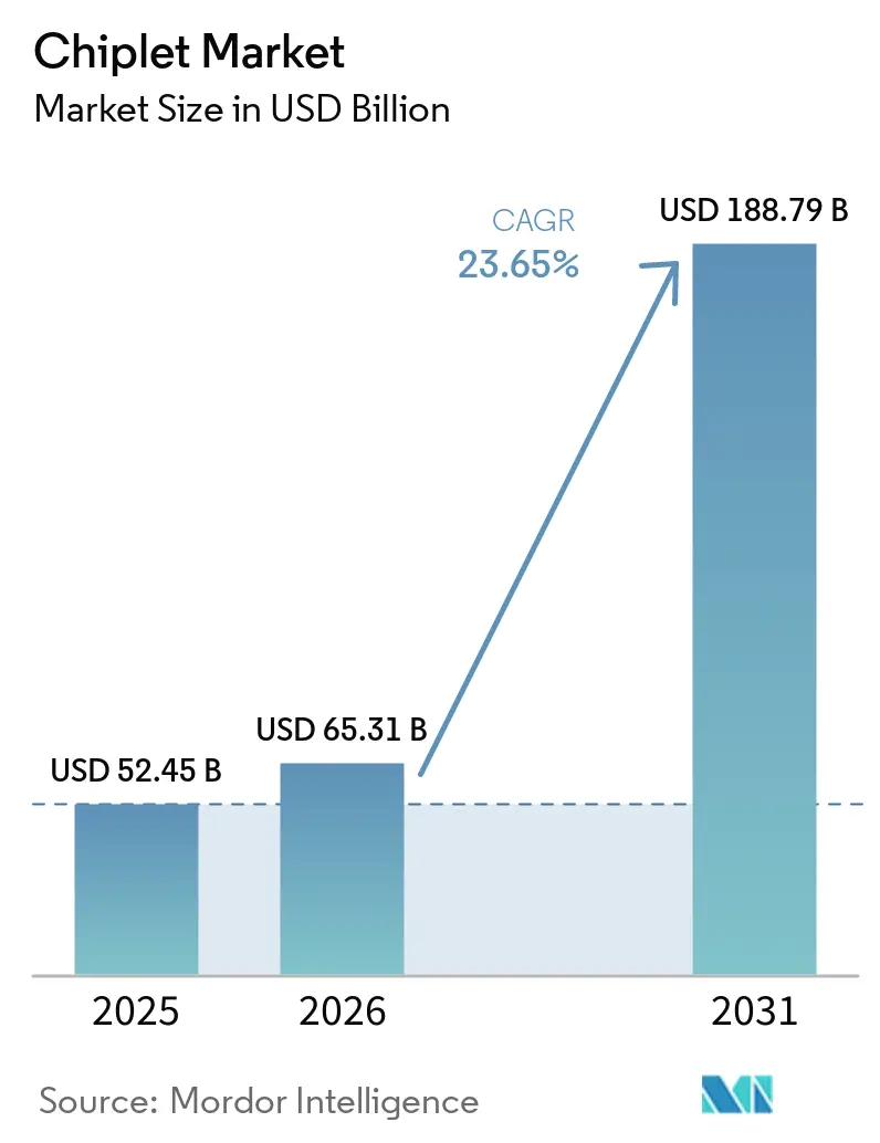
The chiplet market size is projected to be USD 52.45 billion in 2025, USD 65.31 billion in 2026, and reach USD 188.79 billion by 2031, growing at a CAGR of 23.65% from 2026 to 2031. Growth is being shaped by a structural change in semiconductor design economics, as very large leading-edge dies are becoming harder and more expensive to build as single pieces of silicon. Chiplet-based design is also gaining support from faster interconnect standards, especially after the UCIe 3.0 release raised supported data rates and improved manageability for multi-die systems. Demand is strongest where computing density matters most, particularly in AI infrastructure, cloud platforms, and high-performance systems that need more bandwidth and more flexible packaging options. Hybrid bonding and advanced 2.5D and 3D packaging are moving from specialist use toward broader production, which is widening the performance gap between chiplet designs and monolithic alternatives. At the same time, thermal stress, interoperability gaps, and packaging capacity constraints are still slowing deployment in parts of the enterprise market even as long-term demand remains firm.
Key Report Takeaways
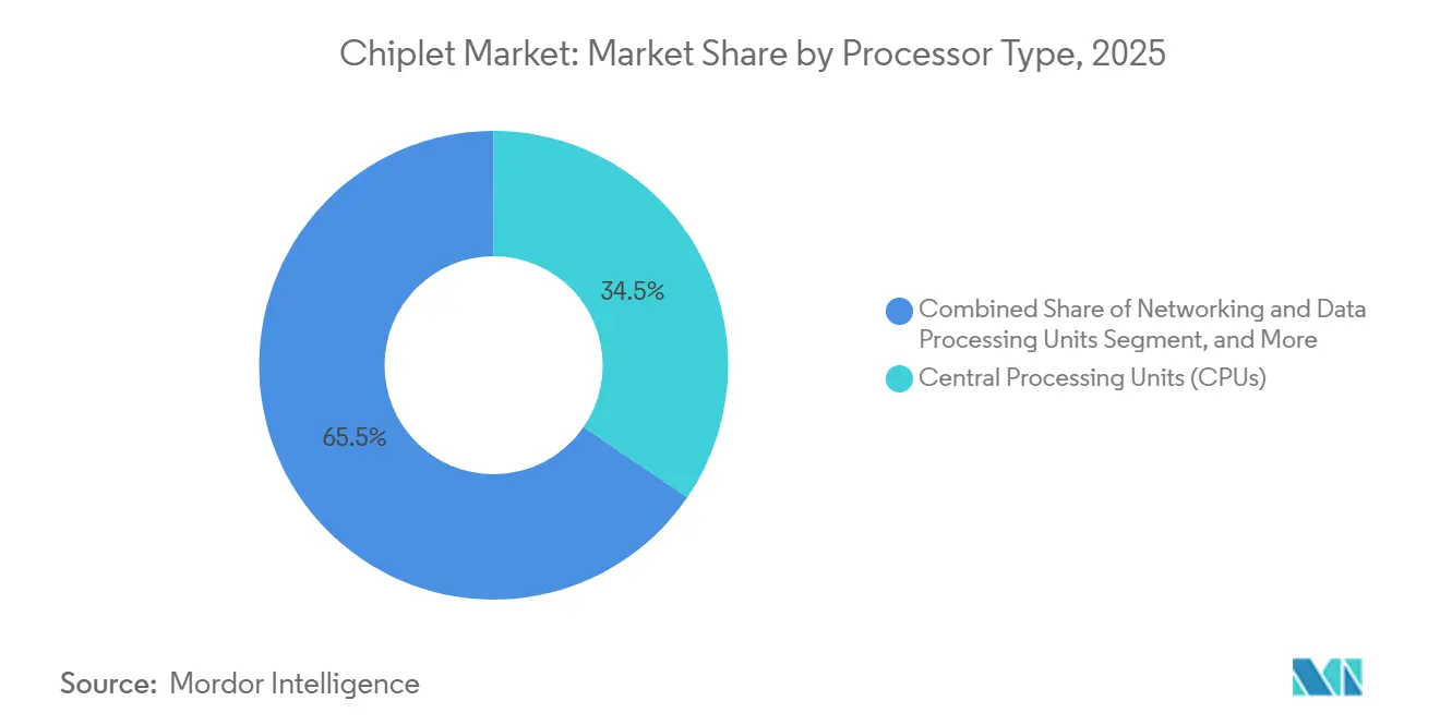
- By processor type, CPUs held 34.54% share of the chiplet market in 2025, while AI accelerator ASICs are projected to expand at a 25.43% CAGR through 2031.
- By packaging technology, 2.5D Interposer and Bridge-Based Packaging accounted for 37.71% share of the chiplet market in 2025, while 3D Stacked and Hybrid-Bonded Packaging is projected to grow at a 24.76% CAGR through 2031.
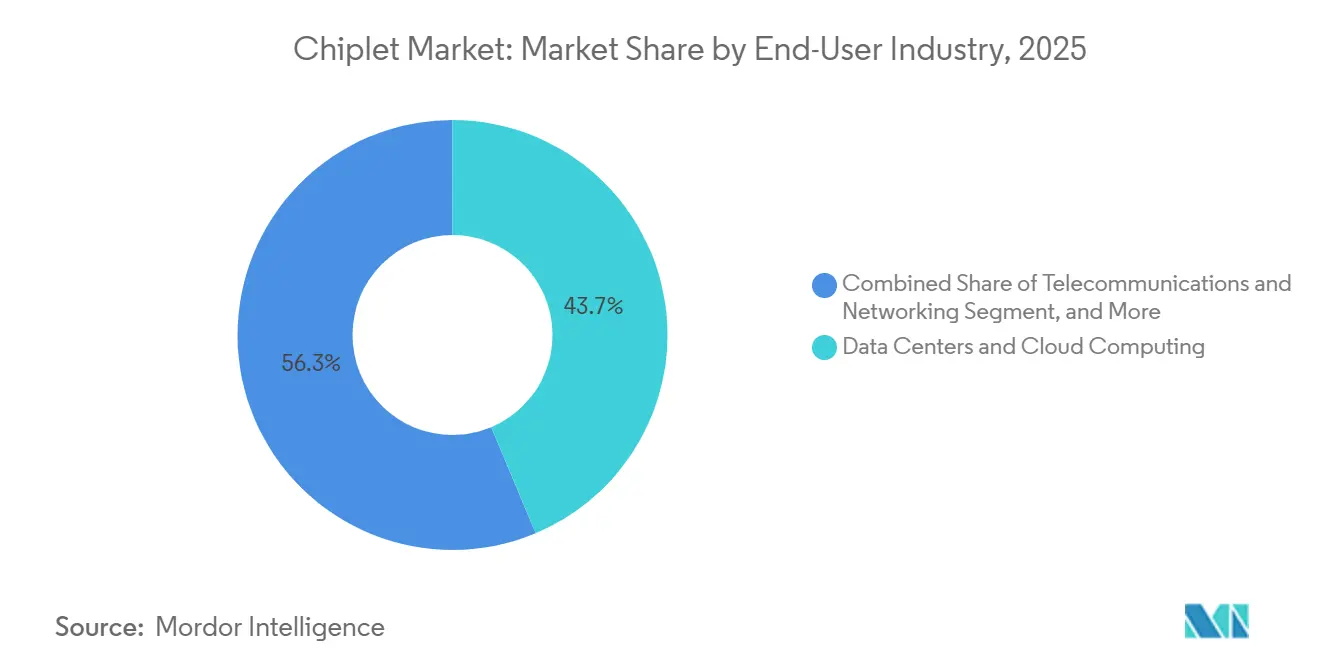
- By end-user industry, Data Centers and Cloud Computing captured 43.67% share of the chiplet market in 2025 and are projected to expand at a 25.92% CAGR through 2031.
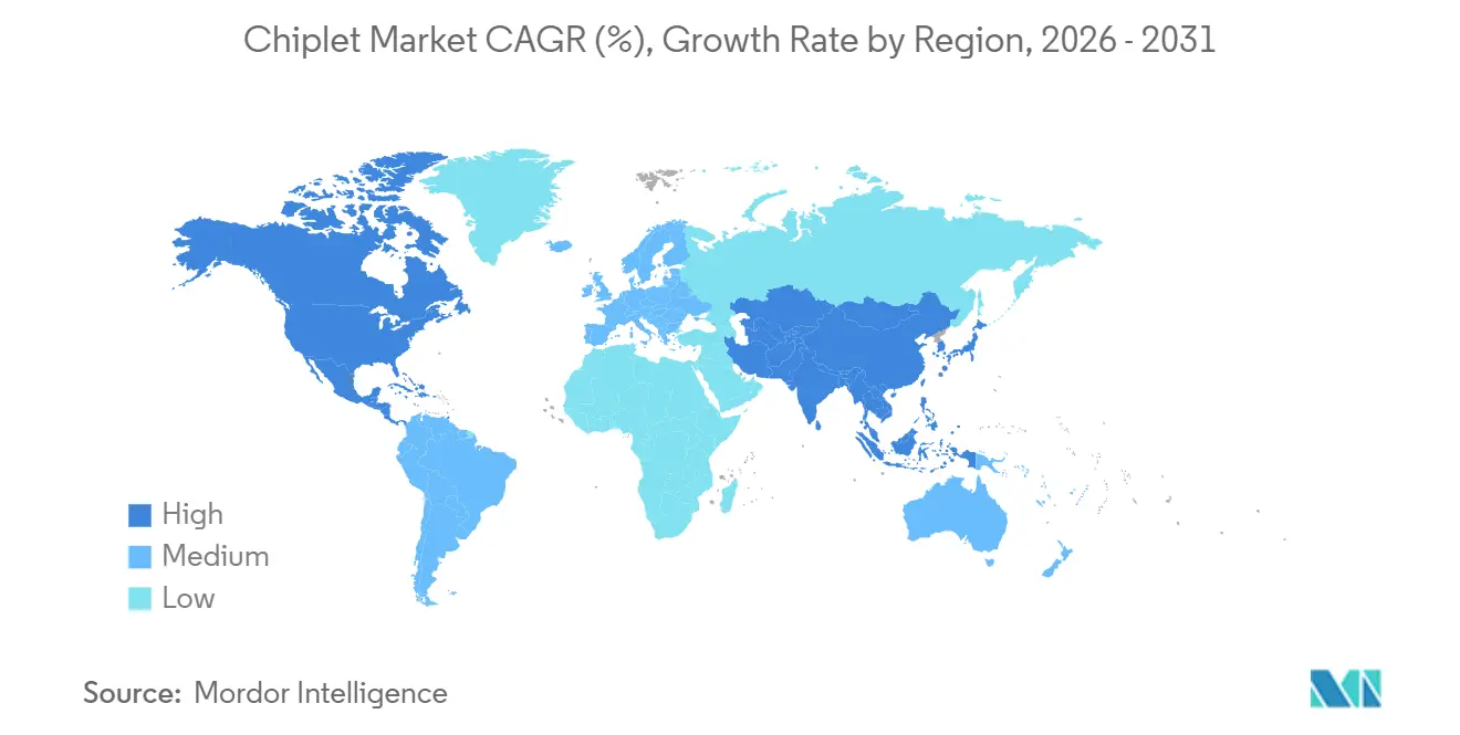
- By geography, Asia-Pacific held 35.93% of the chiplet market share in 2025, while North America is projected to record the highest CAGR at 26.41% through 2031.
Note: Market size and forecast figures in this report are generated using Mordor Intelligence’s proprietary estimation framework, updated with the latest available data and insights as of January 2026.
Global Chiplet Market Trends and Insights
Drivers Impact Analysis*
| Driver | (~) % Impact on CAGR Forecast | Geographic Relevance | Impact Timeline |
|---|---|---|---|
| AI And HPC Reticle-Limit Escape | +6.0% | Global, concentrated in North America and Asia-Pacific | Short term (≤ 2 years) |
| HBM-Centered 2.5D and 3D Package Adoption | +4.5% | Asia-Pacific core, spill-over to North America and Europe | Short term (≤ 2 years) |
| Advanced-Node NRE Reduction Through IP Reuse | +4.0% | Global | Medium term (2-4 years) |
| 5G, Cloud, And Networking Demand For Disaggregated Silicon | +3.0% | Global, early gains in North America and East Asia | Medium term (2-4 years) |
| Optical I/O Chiplets For Rack-Scale AI Scale-Up | +2.5% | North America and Asia-Pacific | Medium term (2-4 years) |
| KGD Testing And UCIe Alliances De-Risk Merchant Chiplets | +1.5% | Global | Long term (≥ 4 years) |
| Source: Mordor Intelligence | |||
AI And HPC Reticle-Limit Escape
The chiplet market is being pushed forward by the simple fact that very large AI and HPC processors are no longer practical as single monolithic dies at the leading edge. As compute demand rises, multi-die integration gives designers a way to scale logic, memory access, and I/O without forcing every function onto one oversized piece of silicon. This is why the chiplet market is now closely tied to the server CPU and AI accelerator road map, not just to packaging innovation. AMD said in May 2026 that its 6th Gen EPYC Venice processor entered production on TSMC 2nm technology, which confirms that chiplet-based CPU design remains the proven path into next-generation server silicon.[1]Advanced Micro Devices, “AMD Announces Production Ramp of Next-Generation AMD EPYC Processor ‘Venice’ on TSMC 2nm Process Technology,” AMD Investor Relations, ir.amd.com The chiplet market also benefits because smaller reusable dies lower the economic barrier for companies that cannot fund a full leading-edge system-on-chip program. That cost and yield advantage is turning chiplet design from a high-end option into a core product strategy across advanced compute programs.
HBM-Centered 2.5D And 3D Package Adoption
The chiplet market is also being lifted by the way AI systems now combine compute logic with stacked memory in dense package-level designs. In practice, that means advanced packages are no longer a supporting feature, they are becoming the performance center of the full device. The chiplet market gains from this shift because package architecture now decides bandwidth, latency, and scaling efficiency as much as transistor density does. The UCIe 3.0 specification released in August 2025 doubled supported data rates to 48 GT/s and 64 GT/s, extended sideband reach, and added new manageability features, which makes more demanding multi-die package designs easier to support over time. That improvement matters because memory and logic are increasingly being designed together at package level rather than selected separately late in the process. As a result, the chiplet market is moving toward deeper co-development between accelerator designers, packaging specialists, and memory suppliers.
Advanced-Node NRE Reduction Through IP Reuse
The chiplet market is expanding because modular design reduces the cost of reaching advanced nodes. Instead of building a full custom system-on-chip, vendors can reuse CPU, I/O, security, or interface dies and combine them with a smaller custom accelerator die. That lowers non-recurring engineering pressure and makes the chiplet market more accessible to firms outside the largest hyperscaler and processor groups. Tenstorrent announced its Open Chiplet Atlas Ecosystem in October 2025 as a royalty-free interoperability framework with more than 50 partners, which signals growing support for shared building blocks and more open design entry points.[2]Tenstorrent, “Tenstorrent Announces Open Chiplet Atlas Ecosystem,” Tenstorrent Newsroom, tenstorrent.com The chiplet market should also widen into regulated verticals because reusable validated blocks fit more naturally with structured verification and qualification work. That combination of lower design cost and better reuse is making multi-die development more commercially realistic across a broader customer base.
5G, Cloud, And Networking Demand For Disaggregated Silicon
The chiplet market is not being driven by compute alone, because networking and cloud infrastructure also need disaggregated silicon with high-bandwidth die-to-die links. Modern AI systems depend on GPUs, CPUs, DPUs, switches, NICs, and memory subsystems working together inside one broader platform. That system-level requirement is widening the chiplet market beyond classic processor categories and into rack-scale architecture. NVIDIA introduced the Vera Rubin platform in March 2026 with 7 new chips spanning GPU, CPU, switching, networking, and other functions, showing how chiplet-style system decomposition is moving into full AI infrastructure design. NVIDIA and Marvell also announced an NVLink Fusion partnership in March 2026, with NVIDIA committing USD 2 billion to Marvell, which underlines the commercial value of custom networking and XPU integration inside next-generation AI factory deployments.[3]Marvell Technology, “NVIDIA AI Ecosystem Expands as Marvell Joins Forces Through NVLink Fusion,” Marvell Investor Relations, investor.marvell.com The chiplet market therefore has a strong second demand engine in network fabrics and cloud infrastructure, not only in general-purpose compute.
Restraints Impact Analysis*
| Restraint | (~) % Impact on CAGR Forecast | Geographic Relevance | Impact Timeline |
|---|---|---|---|
| Thermal And Power-Delivery Bottlenecks In Dense Packages | -3.0% | Global | Short term (≤ 2 years) |
| Immature Cross-Vendor Interoperability And IP Liability | -2.5% | Global | Medium term (2-4 years) |
| Yield Compounding And Test-Cost Inflation In KGD Flows | -2.0% | Global, concentrated in Asia-Pacific fab hubs | Medium term (2-4 years) |
| CoWoS, Interposer, Substrate, And Optical-Packaging Bottlenecks | -1.5% | Asia-Pacific core, spill-over to North America | Short term (≤ 2 years) |
| Source: Mordor Intelligence | |||
Thermal And Power-Delivery Bottlenecks In Dense Packages
The chiplet market faces a clear engineering limit in thermal management as more compute and memory are packed into the same footprint. Dense 2.5D and 3D package designs create heat loads that standard cooling approaches struggle to handle outside the largest data center environments. This is a direct restraint on the chiplet market because deployment can be delayed even when the silicon itself is ready for shipment. A February 2026 study in Materials showed that intelligent thermal optimization for chiplet-based heterogeneous packages improved thermal resistance by 31% and pressure drop by 42% at 500 W/cm², but it still depended on embedded microfluidic structures rather than conventional cooling methods.[4]Xiaoming Li et al., “Research on Intelligent Thermal Optimization for Chiplet-Based Heterogeneously Integrated AI Chip Embedded With Leaf-Vein-Inspired Fractal Microchannels,” Materials, mdpi.com A July 2025 paper in Scientific Reports also showed that electrothermal co-optimization in 2.5D power networks can cut error rates below 4%, though it adds significant manufacturing complexity and cost.[5]Haoran Zhang et al., “Electrothermal Co-Optimization of 2.5D Power Distribution Network With TTSV Cooling,” Scientific Reports, nature.com The result is that the chiplet market remains strongest in hyperscale settings, while broader enterprise rollout still depends on better thermal and power-delivery solutions.
Immature Cross-Vendor Interoperability And IP Liability
The chiplet market is moving faster on electrical standards than on commercial accountability. Even when two chiplets can connect, buyers still need clarity on warranty responsibility, failure analysis, and IP exposure when different vendors are involved in the same package. That uncertainty slows adoption in the chiplet market because enterprise and regulated customers do not want technical openness without clear commercial ownership. UCIe 3.0 improved manageability, runtime recalibration, sideband reach, and emergency shutdown support, which helps the technical side of multi-vendor operation. The UCIe ecosystem now includes major companies such as AMD, Intel, Samsung, and TSMC, which shows strong strategic backing for common interoperability even if full merchant plug-and-play is still developing.[6]UCIe Consortium, “Chiplet Summit 2026, UCIe Momentum Across a Growing Ecosystem,” UCIe Consortium, uciexpress.org Until liability rules and qualification norms mature further, the chiplet market will continue to favor captive ecosystems and tightly managed partnerships over open mix-and-match deployments.
*Our forecasts treat driver/restraint impacts as directional, not additive. The impact forecasts reflect baseline growth, mix effects, and variable interactions.
Segment Analysis
By Processor Type: CPU Installed Base Anchors Share And ASICs Define The Growth Trajectory
CPUs held 34.54% of chiplet market share in 2025, while AI accelerator ASICs are projected to grow at a 25.43% CAGR through 2031. That leadership reflects the scale of the existing server CPU base and the fact that chiplet-based CPU layouts are already proven in cloud and enterprise deployments. The chiplet market has therefore leaned on CPUs for near-term revenue while using AI ASICs as the main forward growth engine. AMD’s continuing EPYC road map, including the May 2026 production ramp for Venice on TSMC 2nm, shows that advanced server CPUs still rely on chiplet partitioning to move into the next node generation. The chiplet market also benefits because CPU platforms give buyers a familiar validation path, which lowers adoption risk when compared with completely new accelerator categories.
AI accelerator ASICs are expanding faster because hyperscalers want silicon tuned for specific training and inference workloads rather than only general-purpose compute. That pushes the chiplet market toward custom compute tiles, specialized memory arrangements, and tighter package-level optimization for each deployment profile. GPUs still retain major revenue weight in AI training, yet the line between GPUs, CPUs, DPUs, LPUs, and other accelerators is becoming less distinct. NVIDIA’s Vera Rubin platform combines multiple processor classes inside one system architecture, which shows how heterogeneous integration is blurring the old processor type boundaries.[7]NVIDIA Corporation, “NVIDIA Vera Rubin Opens Agentic AI Frontier,” NVIDIA Newsroom, nvidianews.nvidia.com The chiplet industry is therefore moving toward mixed processor platforms rather than clean single-category products.



By Packaging Technology: 2.5D Interposer Retains Lead As Hybrid Bonding Reshapes The Next Wave
2.5D Interposer and Bridge-Based Packaging accounted for 37.71% of chiplet market size in 2025, while 3D Stacked and Hybrid-Bonded Packaging is projected to expand at a 24.76% CAGR through 2031. The current lead for 2.5D reflects its better commercial maturity, broader tooling base, and stronger fit for today’s AI accelerator and high-end CPU programs. In the chiplet market, 2.5D remains the practical volume platform because it balances performance with manufacturability better than more aggressive 3D schemes. The UCIe 3.0 release supports this position because higher supported data rates and improved manageability extend what designers can do inside advanced multi-die package layouts before needing a full shift to more complex 3D logic stacking. That means the chiplet market should continue to rely on 2.5D as the main assembly path even while the next generation of package formats gains momentum.
At the same time, hybrid bonding is reshaping the long-term direction of packaging because it supports tighter vertical integration and better interconnect density. This gives the chiplet market a path toward lower latency and higher bandwidth without simply enlarging interposers or substrate footprints. Optical and high-speed die-to-die links are also widening the role of advanced package design in future scale-up systems. Ayar Labs said in September 2025 that it partnered with Alchip Technologies to integrate TeraPHY UCIe optical I/O chiplets into Alchip’s high-performance ASIC designs, which shows how advanced packaging is extending beyond electrical interconnects alone.[8]Ayar Labs, “Ayar Labs and Alchip to Scale AI Infrastructure With Co-Packaged Optics,” Ayar Labs News, ayarlabs.com The chiplet industry is therefore keeping 2.5D as the present workhorse while preparing 3D and optical package models for the next performance step.
By End-User Industry: Data Centers Command Share And Speed
Data Centers and Cloud Computing held 43.67% of the chiplet market size in 2025 and are projected to grow at a 25.92% CAGR through 2031. This rare combination of largest share and fastest growth shows that AI infrastructure spending still has room to expand rather than merely replace older systems. The chiplet market is centered on data centers because that is where buyers are willing to pay for higher bandwidth density, larger memory pools, and more advanced cooling solutions. NVIDIA said in March 2026 that major cloud providers and AI developers were lined up for Vera Rubin deployments, which confirms that next-generation chiplet-heavy systems are being absorbed first by large-scale compute operators. The chiplet market also gains from a dual-track sourcing model in which hyperscalers buy merchant platforms while funding their own custom ASIC programs.
That same concentration creates allocation risk for smaller end users because premium advanced packaging capacity tends to be claimed first by the largest AI infrastructure buyers. High-performance computing remains an important second demand pool, especially in science, defense, and simulation workloads where compute density and memory proximity matter. Automotive and mobility are still earlier-stage users, but chiplet architectures fit the move toward more centralized vehicle electronics and stricter validation requirements. Industrial, edge AI, and aerospace applications are smaller by volume, yet they stay attractive in the chiplet market because they reward known good die discipline, long qualification cycles, and specialized performance targets.[9]JEDEC Solid State Technology Association, “Procurement Standard for Known Good Die,” JEDEC, jedec.org The chiplet market is therefore broadening by application, but its value base remains firmly anchored in cloud and data center demand.
Geography Analysis
Asia-Pacific held 35.93% of chiplet market share in 2025, which made it the largest regional base for the chiplet market. The region leads because Taiwan remains central to advanced foundry output and package integration, while South Korea adds major memory and packaging capability. The chiplet market also depends on the depth of Asia-Pacific’s OSAT and substrate ecosystem, which supports scale production in ways few other regions can match. AMD’s May 2026 update on Venice production at TSMC 2nm reinforces Taiwan’s role as the core execution hub for advanced server chip programs. Japan is strengthening its position in the chiplet market through equipment, materials, and packaging capacity as the regional supply chain moves deeper into advanced-node manufacturing. SEAJ projected that Japan’s domestic semiconductor equipment market would grow 22% in fiscal 2026, which points to a stronger local pipeline for future packaging and chip fabrication capability.[10]Japan Semiconductor Equipment Association, “Semiconductor and FPD Manufacturing Equipment Forecast,” SEAJ, seaj.or.jp
North America is projected to expand at a 26.41% CAGR through 2031, making it the fastest-growing geography in the chiplet market. Growth is being driven by the concentration of hyperscalers, fabless chip companies, advanced system designers, and policy-led investment in domestic semiconductor capacity. The chiplet market is especially active in North America because many of the companies defining AI system architecture are based there, even when manufacturing still spans Asia-Pacific. Ayar Labs closed a USD 500 million Series E round in March 2026 and said it would use the funding to accelerate production of co-packaged optics and expand operations in Taiwan, which captures the region’s role as a design and capital center connected to Asian manufacturing execution. The NVIDIA and Marvell NVLink Fusion partnership announced in March 2026 also highlights how the chiplet market in North America is being shaped by platform alliances around custom XPUs, networking, and photonics.
Europe holds a smaller position in the chiplet market, yet it is becoming more relevant through automotive, industrial, aerospace, and secure-compute use cases. The region’s demand profile favors validated and application-specific multi-die solutions rather than sheer shipment scale. South America and the Middle East and Africa remain early-stage participants in the chiplet market, with demand tied mostly to imported AI infrastructure and cloud data center build-outs. These regions are still modest today, but they should become more visible as hyperscaler reach expands and advanced compute platforms spread into more end markets.

Competitive Landscape
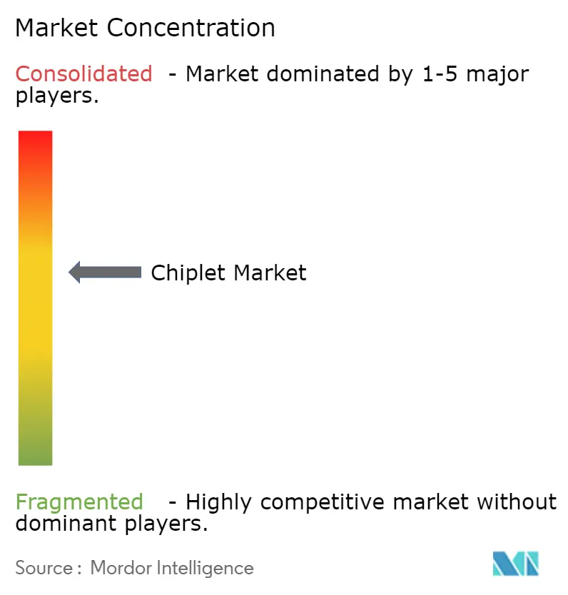
The chiplet market is moderately concentrated in manufacturing and advanced packaging, but much more fragmented in design, IP, and system integration. A small group of companies still controls the most critical execution layers, especially where leading-edge foundry capacity and advanced package assembly are involved. At the same time, the chiplet market includes a wide field of fabless designers, ASIC specialists, interface IP providers, and platform startups competing around different parts of the value chain. This split explains why pricing power and capacity control remain concentrated even as product innovation is widely distributed. It also means the chiplet market can look concentrated from a manufacturing view and fragmented from a product-development view without any contradiction.
Large incumbents such as AMD, Intel, NVIDIA, and Broadcom still operate mainly through captive or tightly managed architectures, which protects performance and integration quality but limits open silicon reuse. The chiplet market therefore remains shaped by proprietary fabrics and internal design rules even while open standards continue to mature. AMD’s 2026 Venice production ramp on TSMC 2nm is one example of a strategic move centered on sustained leadership in chiplet-based server CPUs. NVIDIA’s March 2026 Vera Rubin launch is another example, because it showed how the company is expanding beyond GPUs into a broader rack-scale architecture that combines multiple specialized chips in one platform. Marvell’s NVLink Fusion partnership with NVIDIA added a third example, showing how the chiplet market is opening room for custom XPU and networking suppliers inside larger AI infrastructure ecosystems.
Open ecosystem challengers are becoming more important because they lower the entry barrier for customers that do not want fully captive stacks. Tenstorrent’s Open Chiplet Atlas Ecosystem and Ayar Labs’ optical I/O partnerships both point to a chiplet market that is trying to build reusable building blocks around interfaces, packaging, and subsystem integration. UCIe is also becoming a de facto qualification signal because buyers increasingly want some path toward interoperability even when they still choose curated multi-vendor combinations. The chiplet market should stay moderately concentrated in supply execution, while competition remains intense in architecture, system design, and interface-led differentiation.
Chiplet Industry Leaders
Advanced Micro Devices, Inc.
Intel Corporation
NVIDIA Corporation
Taiwan Semiconductor Manufacturing Company Limited
Samsung Electronics Co., Ltd.
- *Disclaimer: Major Players sorted in no particular order

Recent Industry Developments
- May 2026: AMD announced the production ramp of its 6th Gen EPYC "Venice" processor on TSMC's 2nm technology, marking the first HPC product to enter production at the 2nm node. Future production plans include TSMC's Arizona facility, signaling AMD's commitment to US-based advanced-node chiplet fabrication as a supply-chain resilience strategy.
- May 2026: NVIDIA and Marvell Technology announced a strategic partnership via NVLink Fusion, with NVIDIA committing a USD 2 billion investment in Marvell. The collaboration enables Marvell custom XPUs and NVLink Fusion-compatible networking to integrate into NVIDIA AI factory infrastructure, and includes joint development in silicon photonics
- March 2026: Ayar Labs closed a USD 500 million Series E funding round led by Neuberger Berman, bringing total funding to USD 870 million and valuation to USD 3.75 billion. New investors include MediaTek, Alchip Technologies, and Qatar Investment Authority. The funds are earmarked for scaling TeraPHY UCIe optical chiplet production and expanding operations in Hsinchu, Taiwan.
- March 2026: NVIDIA launched the Vera Rubin platform at GTC 2026, comprising 7 new chips in full production, including the Vera CPU purpose-built for agentic AI. Initial deliveries of Vera CPUs went to Anthropic, OpenAI, SpaceXAI, and Oracle Cloud Infrastructure, with cloud availability from AWS, Google Cloud, Microsoft Azure, and others in the second half of 2026.


Global Chiplet Market Report Scope
The Chiplet Market Report is Segmented by Processor Type (Central Processing Units (CPUs), Graphics Processing Units (GPUs), AI Accelerator ASICs, Field-Programmable Gate Arrays (FPGAs) and Adaptive SoCs, Networking and Data Processing Units (NPUs/DPUs), and Other Chiplet-Based Processor Types), Packaging Technology (2.5D Interposer/Bridge-Based Packaging, 3D Stacked/Hybrid-Bonded Packaging, Fan-Out/RDL-Based Advanced Packaging, Organic Substrate-Based Multi-Die Packaging, and Other Packaging Technologies), End-user Industry (Data Centers and Cloud Computing, High-Performance Computing, Consumer Computing, Automotive and Mobility, Telecommunications and Networking, Industrial and Edge AI, Aerospace and Defense, and Other End-user Industries), and Geography (North America, Europe, Asia-Pacific, South America, and Middle East and Africa). The Market Forecasts in Provided in Terms of Value (USD).
| Central Processing Units (CPUs) |
| Graphics Processing Units (GPUs) |
| AI Accelerator ASICs |
| Field-Programmable Gate Arrays (FPGAs) and Adaptive SoCs |
| Networking and Data Processing Units (NPUs/DPUs) |
| Other Chiplet-Based Processor Types |
| 2.5D Interposer/Bridge-Based Packaging |
| 3D Stacked/Hybrid-Bonded Packaging |
| Fan-Out/RDL-Based Advanced Packaging |
| Organic Substrate-Based Multi-Die Packaging |
| Other Packaging Technologies |
| Data Centers and Cloud Computing |
| High-Performance Computing |
| Consumer Computing |
| Automotive and Mobility |
| Telecommunications and Networking |
| Industrial and Edge AI |
| Aerospace and Defense |
| Other End-user Industries |
| North America | United States |
| Canada | |
| Mexico | |
| Europe | Germany |
| United Kingdom | |
| France | |
| Italy | |
| Rest of Europe | |
| Asia-Pacific | China |
| Japan | |
| South Korea | |
| Taiwan | |
| India | |
| Rest of Asia-Pacific | |
| South America | Brazil |
| Argentina | |
| Rest of South America | |
| Middle East and Africa | United Arab Emirates |
| Saudi Arabia | |
| South Africa | |
| Rest of Middle East and Africa |
| By Processor Type | Central Processing Units (CPUs) | |
| Graphics Processing Units (GPUs) | ||
| AI Accelerator ASICs | ||
| Field-Programmable Gate Arrays (FPGAs) and Adaptive SoCs | ||
| Networking and Data Processing Units (NPUs/DPUs) | ||
| Other Chiplet-Based Processor Types | ||
| By Packaging Technology | 2.5D Interposer/Bridge-Based Packaging | |
| 3D Stacked/Hybrid-Bonded Packaging | ||
| Fan-Out/RDL-Based Advanced Packaging | ||
| Organic Substrate-Based Multi-Die Packaging | ||
| Other Packaging Technologies | ||
| By End-user Industry | Data Centers and Cloud Computing | |
| High-Performance Computing | ||
| Consumer Computing | ||
| Automotive and Mobility | ||
| Telecommunications and Networking | ||
| Industrial and Edge AI | ||
| Aerospace and Defense | ||
| Other End-user Industries | ||
| By Geography | North America | United States |
| Canada | ||
| Mexico | ||
| Europe | Germany | |
| United Kingdom | ||
| France | ||
| Italy | ||
| Rest of Europe | ||
| Asia-Pacific | China | |
| Japan | ||
| South Korea | ||
| Taiwan | ||
| India | ||
| Rest of Asia-Pacific | ||
| South America | Brazil | |
| Argentina | ||
| Rest of South America | ||
| Middle East and Africa | United Arab Emirates | |
| Saudi Arabia | ||
| South Africa | ||
| Rest of Middle East and Africa | ||


Key Questions Answered in the Report
What is the current and forecast value of the chiplet sector?
The chiplet market size is projected at USD 65.31 billion in 2026 and is forecast to reach USD 188.79 billion by 2031, growing at a 23.65% CAGR over 2026-2031.
Which processor category leads demand for chiplet-based products?
CPUs held the largest share at 34.54% in 2025 because server platforms already use chiplet-based CPU designs at scale, while AI accelerator ASICs are growing faster.
Which packaging technology is used the most today?
2.5D Interposer and Bridge-Based Packaging led with 37.71% share in 2025 because it offers the best balance of maturity, performance, and manufacturability for current AI and server products.
Why are data centers driving so much demand?
Data Centers and Cloud Computing held 43.67% share in 2025 and are projected to grow at a 25.92% CAGR because AI workloads need high bandwidth, dense memory integration, and advanced package designs.
Which region is growing the fastest for chiplet adoption?
North America is projected to post the fastest growth at a 26.41% CAGR through 2031, supported by hyperscaler demand, fabless design activity, and domestic semiconductor investment.
What are the main risks slowing broader adoption?
Thermal stress in dense packages, incomplete cross-vendor interoperability, and packaging supply constraints remain the main barriers, especially outside hyperscale deployments.
Page last updated on: