Advanced Packaging Market Size and Share
Market Overview
| Study Period | 2019 - 2030 |
|---|---|
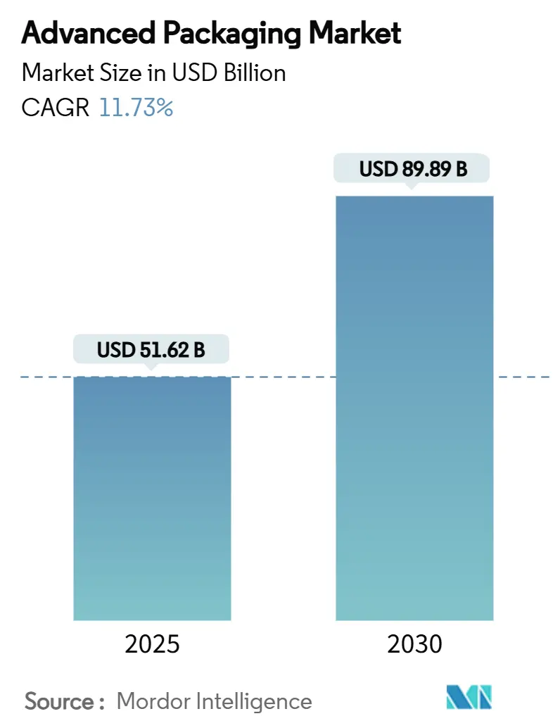
| Market Size (2025) | USD 51.62 Billion |
| Market Size (2030) | USD 89.89 Billion |
| Growth Rate (2025 - 2030) | 11.73% CAGR |
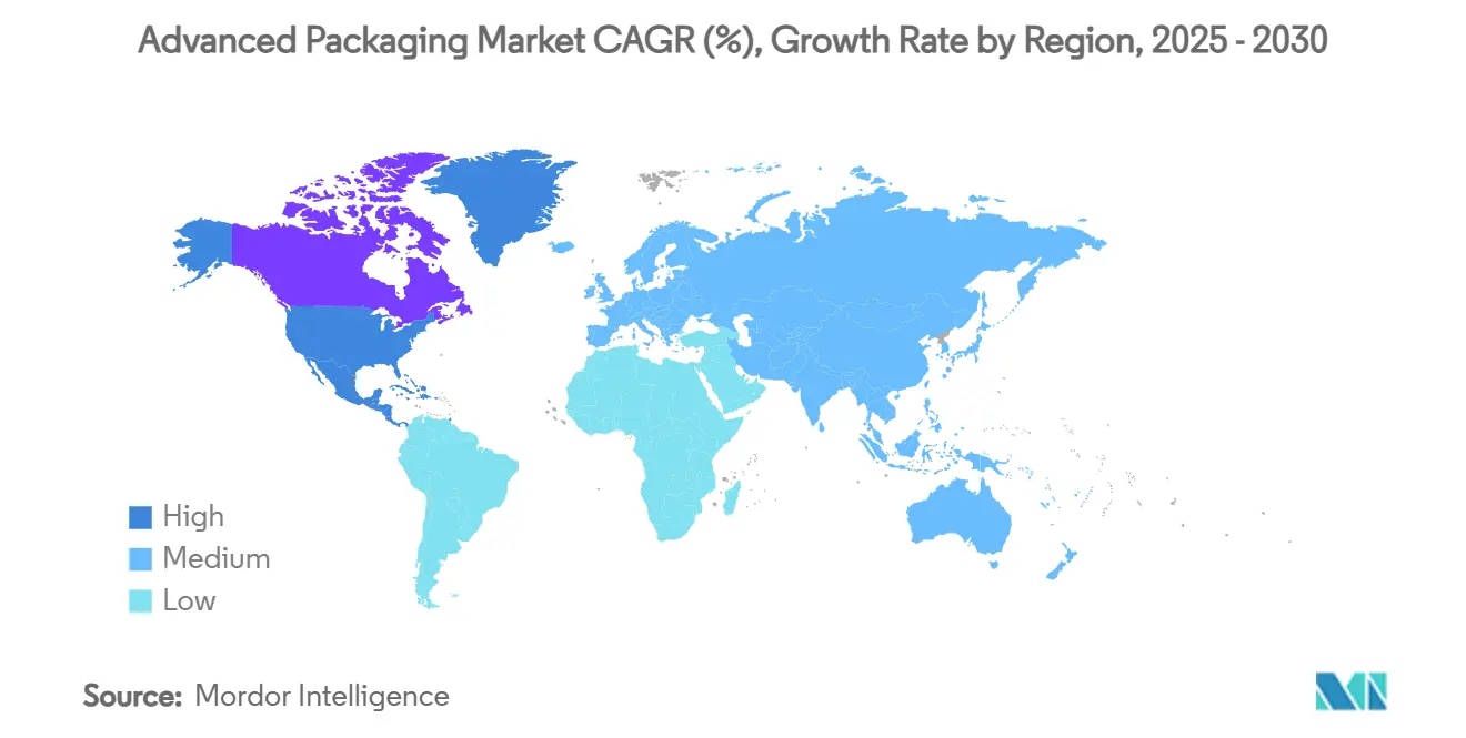
| Fastest Growing Market | North America |
| Largest Market | Asia Pacific |
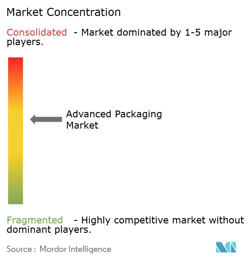
| Market Concentration | Medium |
Major Players
*Disclaimer: Major Players sorted in no particular order Image © Mordor Intelligence. Reuse requires attribution under CC BY 4.0. |
|
Advanced Packaging Market Analysis by Mordor Intelligence
The advanced packaging market size was valued at USD 51.62 billion in 2025 and is forecast to expand at an 11.73% CAGR to reach USD 89.89 billion by 2030. Demand outpaced earlier projections because heterogeneous integration became indispensable for artificial-intelligence (AI) processors that exceed the thermal and interconnect limits of conventional packages. In response, integrated-device manufacturers (IDMs) and outsourced semiconductor assembly and test (OSAT) providers accelerated capital spending, while governments earmarked large incentives to localize assembly capacity. The advanced packaging market also benefited from glass-core substrate R&D, panel-level processing pilots, and the rapid adoption of co-packaged optics in hyperscale data centers. Supply remained tight, however, as BT-resin substrate shortages and scarce engineering talent hindered timely capacity additions. Competitive intensity rose as foundries internalized packaging to secure end-to-end control of AI supply chains, squeezing traditional OSAT margins and prompting strategic specialization.
Key Report Takeaways
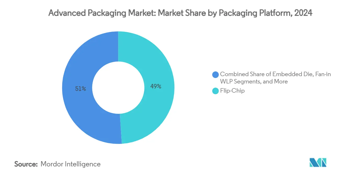
- By packaging platform, flip-chip technology led with 49.0% revenue in 2024, whereas 2.5D/3D solutions are projected to advance at a 13.2% CAGR through 2030.
- By end-user industry, consumer electronics held 40.0% of demand in 2024; automotive and electric-vehicle applications are poised for a 12.4% CAGR to 2030.
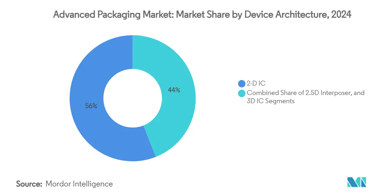
- By device architecture, 2D ICs accounted for a 56.0% share in 2024, while 3D IC technologies are forecast to grow at a 15.1% CAGR.
- By interconnect technology, solder bumps commanded 62.0% of the advanced packaging market share in 2024; hybrid bonding is expected to post a 17.5% CAGR.
- By geography, Asia-Pacific captured 75.0% of 2024 revenue; North America represents the fastest-growing region at a 12.5% CAGR, enabled by CHIPS Act funding.
Global Advanced Packaging Market Trends and Insights
Drivers Impact Analysis
| Driver | (~) % Impact on CAGR Forecast | Geographic Relevance | Impact Timeline |
|---|---|---|---|
| Rising demand for heterogeneous integration for AI and HPC | +3.2% | Global, concentrated in North America and Asia-Pacific | Medium term (2-4 years) |
| Miniaturization of consumer devices is boosting WLP adoption | +2.1% | Global, led by Asia-Pacific manufacturing hubs | Short term (≤ 2 years) |
| Government semiconductor subsidies (e.g., CHIPS, EU Chips Act) | +1.8% | North America, Europe, and select Asia-Pacific regions | Long term (≥ 4 years) |
| EV power-electronics reliability needs (advanced power packages) | +1.5% | Global, early gains in China, Germany, United States | Medium term (2-4 years) |
| Emerging glass-core substrates enabling panel-level packaging | +1.3% | Asia-Pacific core, spill-over to North America | Long term (≥ 4 years) |
| Co-packaged optics demand in hyperscale data centers | +1.8% | Global, concentrated in major datacenter regions | Medium term (2-4 years) |
| Source: Mordor Intelligence | |||
Rising demand for heterogeneous integration for AI and HPC
AI workloads require compute density and memory bandwidth unattainable with legacy packaging. TSMC’s CoWoS platform integrates chiplets and high-bandwidth memory in a single structure, gaining rapid adoption among leading AI accelerator vendors.[1]Taiwan Semiconductor Manufacturing Company Limited, “TSMC Intends to Expand Its Investment in the United States to US USD165 Billion to Power the Future of AI,” pr.tsmc.com Samsung’s SAINT technology achieved similar objectives using hybrid bonding that supports forthcoming HBM4 stacks, underscoring the strategic value of in-house advanced packaging. Thermal interface materials, specialized substrates, and active interposers raised package cost to 15–20% of the total semiconductor build-to-materials, up from 5–8% for mainstream CPUs. As a result, advanced packaging capacity became as critical as leading-edge fabs in determining time-to-market for AI systems. The advanced packaging market, therefore, grew in tandem with, rather than lagging, front-end process migrations.
Miniaturization of consumer devices boosting WLP adoption
Smartphones, wearables, and hearables consistently demand thinner profiles and higher functional density. Fan-out wafer-level packaging (FOWLP) enables multiple dies to be embedded in ultra-thin packages below 0.5 mm, supporting flagship mobile processors without compromising thermal performance. The shift from fan-in WLP to FOWLP reduced overall system cost by up to 25% because under-fill, wire-bonding, and laminate substrates were eliminated. Miniaturization also moved into implantable medical electronics, where dimensions are life-critical; leadless pacemakers benefited from WLP to cut device size by 93% while meeting stringent reliability targets. Consequently, consumer and medical demand created a recurring baseline that insulated the advanced packaging market from cyclical swings in PC end-markets.
Government semiconductor subsidies accelerating infrastructure development
Legislation such as the United States CHIPS and Science Act allocated USD 52.7 billion for domestic capability, with USD 1.6 billion reserved for advanced packaging. Amkor secured USD 407 million to build a USD 2 billion facility in Arizona, the largest OSAT investment on U.S. soil. Europe followed with a EUR 43 billion (~USD 48.6 billion) Chips Act, catalyzing onsemi’s USD 2 billion vertically integrated silicon-carbide packaging site in the Czech Republic. Singapore approved substantial incentives for Micron’s USD 7 billion high-bandwidth memory packaging plant, creating 3,000 jobs by 2027. Subsidies shifted comparative advantage away from the traditional low-cost hubs toward politically prioritized geographies, reshaping site-selection decisions for new lines in the advanced packaging market.
EV power-electronics reliability transforming packaging requirements
The migration to 800-volt vehicle architectures forced radical improvements in thermal, voltage, and mechanical robustness. JCET committed RMB 4.4 billion (USD 621 million) to build an automotive-grade packaging campus in Shanghai dedicated to silicon-carbide and high-temperature components. Packages designed for EV inverters must withstand −40 °C to +150 °C thermal cycling over 20 years, a requirement that dictates advanced materials, void-free sintering, and double-sided cooling topologies. Automotive silicon-carbide modules now carry package value three to four times that of traditional silicon devices, elevating packaging from commodity to differentiation. Tier-1 suppliers consequently entered co-development agreements with OSATs to secure proprietary designs, supporting sustained double-digit revenue growth for automotive lines within the advanced packaging market.
Restraints Impact Analysis
| Restraint | (~) % Impact on CAGR Forecast | Geographic Relevance | Impact Timeline |
|---|---|---|---|
| High capital intensity of advanced packaging lines | -2.1% | Global, particularly impacting smaller players | Short term (≤ 2 years) |
| Industry consolidation is squeezing outsourced margins | -1.8% | Global, concentrated in Asia-Pacific OSAT hubs | Medium term (2-4 years) |
| BT-resin substrate capacity bottlenecks | -1.5% | Global supply is concentrated in Japan and Taiwan | Short term (≤ 2 years) |
| Shortage of advanced assembly talent | -1.2% | Global, acute in North America and Europe | Long term (≥ 4 years) |
| Source: Mordor Intelligence | |||
High capital intensity constraining market entry
Tooling for 2.5D and 3D processes can cost USD 10–15 million per chamber, vastly exceeding the USD 3 million typical for legacy lines. TSMC budgeted USD 42 billion in 2025 capital outlays, of which a material share targeted advanced packaging expansions. Smaller OSATs, therefore, struggled to amortize investments across rapidly shrinking product life cycles, prompting niche specialization or defensive mergers. The elevated hurdle rate widened the technological gap between tier-one providers and regional followers, dampening fresh capacity in the advanced packaging market during 2024–2026.
BT-resin substrate bottlenecks limiting production capacity
High-density build-up substrates used in 2.5D interposers depend on BT resin supplied by a limited group of Japanese and Taiwanese firms. Lead times doubled to 24 weeks for the most advanced substrates, forcing package redesigns that sacrificed input/output density or increased bill-of-materials expense. To secure supply, leading OSATs structured multi-year purchase agreements and explored backward integration with substrate partners. Until new fabs reach volume in 2026, substrate scarcity remains a gating factor that tempers the otherwise robust growth trajectory of the advanced packaging market.
Segment Analysis
By Packaging Platform: AI workloads accelerate 2.5D/3D adoption
Flip-chip packages retained leadership with 49.0% revenue in 2024, anchored by high-volume consumer and industrial applications. Yet 2.5D/3D configurations delivered the fastest gains, achieving a 13.2% CAGR outlook as AI accelerators demanded logic-to-memory proximity beyond flip-chip limits. The advanced packaging market size for 2.5D/3D solutions is forecast to reach USD 34.1 billion by 2030, equal to 38% of total platform revenue.
Samsung’s SAINT platform attained sub-10 µm hybrid bonds, reducing signal latency by 30% and extending thermal headroom by 40% relative to wire-bonded stacks.[2]SEMI VISION, “Geopolitical Disruption to the Semiconductor Industry Ecosystem,” tspasemiconductor.substack.com TSMC’s CoWoS ramped three additional lines in 2025 to clear a 12-month backlog. Embedded-die and fan-out WLP progressed as complementary options: embedded packages suited space-constrained automotive domains, while fan-out WLP captured 5G base-station and mmWave radar designs. Collectively, these dynamics embedded 2.5D/3D packaging at the center of next-generation device roadmaps, guaranteeing its role as the prime value driver inside the advanced packaging market.
Note: Segment shares of all individual segments available upon report purchase
By End-User Industry: Vehicle electrification widens demand profile
Consumer electronics absorbed 40.0% of 2024 shipments, but its growth plateaued at single digits. In contrast, automotive and EV demand is projected to expand at a 12.4% CAGR, lifting its share of the advanced packaging market to 18% by 2030. The advanced packaging market size for automotive electronics is estimated to surpass USD 16 billion by the end of the forecast period.
EV traction inverters, on-board chargers, and domain controllers now specify automotive-grade fan-out, double-side cooled power modules, and over-molded system-in-package (SiP) assemblies. Data-center infrastructure provided another high-growth niche: AI servers utilize advanced packages with power densities reaching 1,000 W/cm², dictating innovative thermal lid and under-fill chemistries. Healthcare, meanwhile, requires biocompatible coatings and hermetic enclosures, attributes that carry premium average selling prices and stable replacement demand. Cumulatively, these segment trends diversified revenue streams and reduced dependence on cyclical smartphone refresh cycles within the advanced packaging market.
By Device Architecture: Vertical integration extends scaling
Two-dimensional ICs still comprised 56.0% of units in 2024, yet their share is projected to decline as 3D ICs scale at a 15.1% CAGR. The advanced packaging market share for 3D ICs is expected to reach 28% by 2030 as through-silicon-via (TSV) and hybrid-bonded stacks move into mainstream AI and networking devices.
Samsung demonstrated logic-to-memory hybrid cubes that achieved sub-10 µm TSV pitch, improving bandwidth and energy efficiency against 2.5D interposer solutions. At the same time, 2.5D interposers formed a transitional architecture for designers seeking higher performance without full TSV complexity. Foundries and OSATs collaborated on active-interposer programs that embed voltage regulation and photonic layers, signaling a gradual convergence of advanced packaging and system-on-substrate concepts. These architectural shifts ensure vertical integration remains the central lever for sustaining Moore-like progress, cementing its importance to the advanced packaging market.
Note: Segment shares of all individual segments available upon report purchase
By Interconnect Technology: Hybrid bonding overtakes pitch limits
Solder bumps held 62.0% revenue in 2024, reflecting their cost competitiveness for legacy nodes. Copper pillars gained share in performance-driven flip-chip devices, but the fastest acceleration came from hybrid bonds projected at a 17.5% CAGR. The advanced packaging market size attributable to hybrid bonding is expected to reach USD 18.2 billion by 2030, up from USD 6.6 billion in 2024.
Hybrid bonding enables direct metal-to-metal contacts below 10 µm, eliminating under-bump metallization and enhancing thermal paths. Samsung deployed the technique in HBM4 production, cutting signal latency by 40% and doubling bandwidth. Yield learning curves improved significantly in 2025, approaching mature flip-chip levels, which removed a key adoption barrier. As logic-to-memory and die-to-die interfaces climb into multiple terabits per second, hybrid bonding’s scalability positions it as the default choice for next-generation integration across the advanced packaging market.
Geography Analysis
Asia-Pacific generated 75.0% of 2024 revenue because Taiwan, South Korea, and mainland China house the bulk of front-end fabs and substrate suppliers. TSMC announced a USD 165 billion U.S. investment, reflecting a diversification strategy rather than the displacement of its Taiwan base, ensuring Asia retains leadership in the medium term. China’s domestic OSATs delivered double-digit sales gains and expanded into automotive packaging, but tight controls on extreme-ultraviolet (EUV) tools limited their move into leading-edge wafer-fab processes.
North America emerged as the fastest-growing region at a 12.5% CAGR thanks to the CHIPS Act incentives. Amkor’s USD 2 billion Arizona site will combine bump, wafer-level, and panel-level lines once fully ramped in 2027, providing the first large-scale outsourced option near U.S. system integrators. Intel, Apple, and NVIDIA pre-booked a portion of this capacity to de-risk geopolitical supply interruptions, redirecting meaningful volumes that historically flowed to East Asian OSATs. Consequently, the advanced packaging market now includes a credible North American supply node capable of high-volume AI product support.
Europe pursued specialization rather than volume leadership. onsemi’s Czech facility addressed silicon-carbide devices for automotive power, aligning with local OEM electrification targets. Germany’s Fraunhofer institutes led panel-level research, but manufacturers stayed cautious on green-field megasite commitments. Meanwhile, Singapore strengthened its hub role; Micron’s HBM plant and KLA’s process-control expansion created a vertically coherent ecosystem that supports AI memory and metrology under one jurisdiction.[3]Micron Technology, “Micron Breaks Ground on New HBM Advanced Packaging Facility in Singapore,” investors.micron.com India introduced a 50% capital cost-sharing scheme, attracting proposals for advanced packaging pilots that promise medium-term upside yet remain contingent on talent availability.
Collectively, these developments diversified geographic risk for system OEMs and rebalanced the advanced packaging market. Even so, Asia-Pacific is forecast to maintain more than 60% share in 2030 because existing infrastructure, supply clusters, and economies of scale still surpass new regional entrants.
Competitive Landscape
The market shifted from moderate to tight competition as foundries vertically integrated packaging to capture AI value pools. TSMC, Samsung, and Intel all promoted in-house 3D packaging as equal in strategic weight to sub-2 nm wafer technology, eroding the traditional boundary between front-end and back-end operations. OSATs responded by specializing: JCET concentrated on automotive-grade modules, while ASE invested in panel-level fan-out lines tuned for smartphone application processors.
Margin pressure intensified because the capital intensity of 2.5D lines compressed return on invested capital, especially for second-tier providers reliant on commoditized flip-chip revenue. Government grants partly offset capital needs, yet subsidy access favored large incumbents, accelerating consolidation. Several regional OSATs formed joint ventures with substrate manufacturers to lock in supply, illustrating a pivot to vertical control within the advanced packaging market.
Technological differentiation became the dominant competitive axis. Samsung leveraged hybrid bonding to secure HBM4 contracts, beating competitors still qualifying for copper pillar upgrades. Amkor emphasized geographic proximity to U.S. customers through its Arizona facility, trading some cost advantage for geopolitical assurance. JCET’s early-moving focus on automotive reliability standards delivered an 88% revenue jump in 2023 and positioned the company to influence future EV module standards.[4]JCET Group, “JCET's Automotive Chip Advanced Packaging Flagship Factory Project Gains Momentum,” jcetglobal.com These moves collectively raised the technology bar for new entrants, giving incumbents time to absorb their heavy 2024–2025 capex cycles.
Advanced Packaging Industry Leaders
-
Amkor Technology, Inc.
-
Taiwan Semiconductor Manufacturing Company Limited
-
Advanced Semiconductor Engineering Inc.
-
Intel Corporation
-
JCET Group Co. Ltd
- *Disclaimer: Major Players sorted in no particular order
Recent Industry Developments
- March 2025: TSMC announced a USD 165 billion U.S. expansion plan covering three fabs and two advanced packaging facilities.
- January 2025: Micron broke ground on a USD 7 billion high-bandwidth memory packaging plant in Singapore.
- October 2024: KLA completed Phase 1 of a USD 200 million Singapore expansion for process-control solutions.
- July 2024: Amkor received USD 407 million CHIPS Act support for its USD 2 billion Arizona site.
Global Advanced Packaging Market Report Scope
Advanced packaging refers to the aggregation and interconnection of components before traditional integrated circuit packaging. It allows multiple devices, such as electrical, mechanical, or semiconductor components, to be merged and packaged as a single electronic device. Unlike traditional integrated circuit packaging, advanced packaging employs processes and techniques at semiconductor fabrication facilities.
The advanced packaging market is segmented by packaging platform and geography. By packaging platform market is segmented into flip chip, embedded die, Fi-WLP, Fo-WLP, and 2.5D/3D. By geography, the market is segmented into North America, Europe, Asia Pacific, Latin America, and the Middle East and Africa.
The report offers market forecasts and size in value (USD) for all the above segments.
| Flip-Chip |
| Embedded Die |
| Fan-in WLP |
| Fan-out WLP |
| 2.5D / 3D |
| Consumer Electronics |
| Automotive and EV |
| Data Center and HPC |
| Industrial and IoT |
| Healthcare / Med-tech |
| 2D IC |
| 2.5D Interposer |
| 3D IC (TSV / Hybrid-Bond) |
| Solder Bump |
| Copper Pillar |
| Hybrid Bond |
| North America | United States | |
| Canada | ||
| Mexico | ||
| South America | Brazil | |
| Argentina | ||
| Rest of South America | ||
| Europe | Germany | |
| France | ||
| United Kingdom | ||
| Italy | ||
| Netherlands | ||
| Russia | ||
| Rest of Europe | ||
| Asia-Pacific | China | |
| Taiwan | ||
| South Korea | ||
| Japan | ||
| Singapore | ||
| Malaysia | ||
| India | ||
| Rest of Asia-Pacific | ||
| Middle East and Africa | Middle East | Israel |
| United Arab Emirates | ||
| Saudi Arabia | ||
| Turkey | ||
| Rest of Middle East | ||
| Africa | South Africa | |
| Nigeria | ||
| Rest of Africa | ||
| By Packaging Platform | Flip-Chip | ||
| Embedded Die | |||
| Fan-in WLP | |||
| Fan-out WLP | |||
| 2.5D / 3D | |||
| By End-User Industry | Consumer Electronics | ||
| Automotive and EV | |||
| Data Center and HPC | |||
| Industrial and IoT | |||
| Healthcare / Med-tech | |||
| By Device Architecture | 2D IC | ||
| 2.5D Interposer | |||
| 3D IC (TSV / Hybrid-Bond) | |||
| By Interconnect Technology | Solder Bump | ||
| Copper Pillar | |||
| Hybrid Bond | |||
| By Geography | North America | United States | |
| Canada | |||
| Mexico | |||
| South America | Brazil | ||
| Argentina | |||
| Rest of South America | |||
| Europe | Germany | ||
| France | |||
| United Kingdom | |||
| Italy | |||
| Netherlands | |||
| Russia | |||
| Rest of Europe | |||
| Asia-Pacific | China | ||
| Taiwan | |||
| South Korea | |||
| Japan | |||
| Singapore | |||
| Malaysia | |||
| India | |||
| Rest of Asia-Pacific | |||
| Middle East and Africa | Middle East | Israel | |
| United Arab Emirates | |||
| Saudi Arabia | |||
| Turkey | |||
| Rest of Middle East | |||
| Africa | South Africa | ||
| Nigeria | |||
| Rest of Africa | |||
Key Questions Answered in the Report
What is the projected size of the advanced packaging market by 2030?
The market is forecast to reach USD 89.89 billion in 2030, growing at an 11.73% CAGR from its 2025 base.
Which packaging platform is expected to grow the fastest?
2.5D/3D technologies are projected to post a 13.2% CAGR, outpacing flip-chip, fan-out, and embedded-die platforms.
Why is North America the fastest-growing regional market?
CHIPS Act incentives and large private investments such as Amkor’s USD 2 billion Arizona facility are fostering local capacity, driving a 12.5% regional CAGR through 2030.
How do automotive applications influence advanced packaging demand?
Electric-vehicle power electronics and domain controllers require high-reliability packages, resulting in a forecast 12.4% CAGR for automotive and EV applications.
What is hybrid bonding, and why is it important?
Hybrid bonding forms direct metal-to-metal links below 10 µm pitch, enabling higher bandwidth and better thermal performance than traditional solder bumps, making it the fastest-growing interconnect segment at a 17.5% CAGR.
What challenges could slow market growth?
High capital intensity and BT-resin substrate shortages create capacity constraints that could temper short-term expansion.
Page last updated on:


