MEMS Packaging Market Size and Share
Market Overview
| Study Period | 2020 - 2031 |
|---|---|
| Market Size (2026) | USD 8.51 Billion |
| Market Size (2031) | USD 11.99 Billion |
| Growth Rate (2026 - 2031) | 7.12% CAGR |
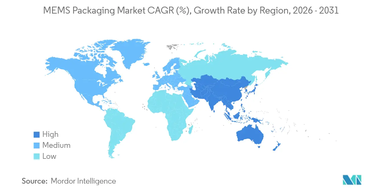
| Fastest Growing Market | Asia Pacific |
| Largest Market | Asia Pacific |
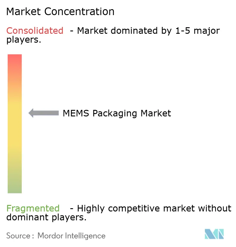
| Market Concentration | Medium |
Major Players *Disclaimer: Major Players sorted in no particular order Image © Mordor Intelligence. Reuse requires attribution under CC BY 4.0. | |
MEMS Packaging Market Analysis by Mordor Intelligence
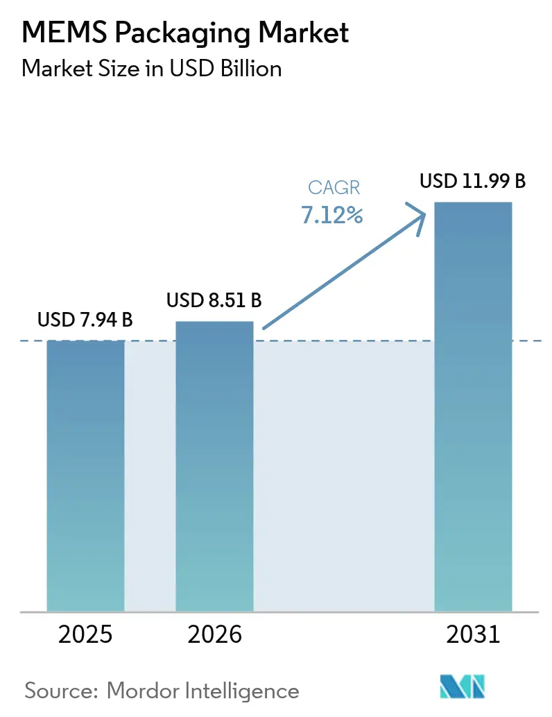
MEMS packaging market size in 2026 is estimated at USD 8.51 billion, growing from 2025 value of USD 7.94 billion with 2031 projections showing USD 11.99 billion, growing at 7.12% CAGR over 2026-2031. This expansion reflects the structural shift from cloud-centric data processing to edge intelligence, where latency-sensitive automotive safety features, on-device AI in smartphones, and hermetically sealed implantable monitors require sub-micron packaging tolerances. Growth is therefore driven less by unit volume and more by the complexity of co-packaging heterogeneous die such as MEMS accelerometers with ASIC signal processors or CMUT ultrasound arrays bonded to CMOS readout chips within footprints that automobile Tier-1 suppliers and phone OEMs now specify in single-digit millimeter dimensions. Asia Pacific leads adoption as 12-inch foundries ramp, while public subsidies in North America and Europe de-risk advanced-packaging investments. On the materials side, glass and ceramic substrates are gaining favor because they match silicon’s thermal expansion and sustain hermetic seals needed for RF MEMS and implantable medical devices.
Key Report Takeaways
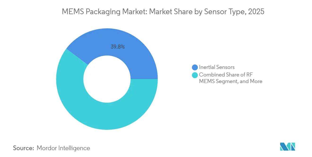
- By sensor type, inertial sensors led with 39.78% of 2025 revenue, while RF MEMS is forecast to grow at an 8.05% CAGR through 2031.
- By packaging platform, wafer-level chip-scale packages captured 44.25% revenue in 2025, and System-in-Package is advancing at a 9.22% CAGR to 2031.
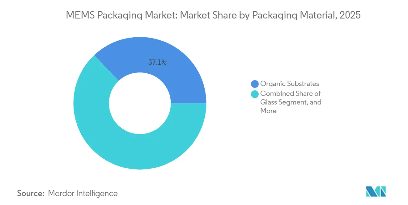
- By packaging material: organic substrates lead, glass substrates surge, and organic laminates captured 37.05% of 2025 revenue due to low material cost and compatibility with flip-chip flows. glass substrates are forecast to grow 10.3% through 2031.
- By geography, Asia Pacific commanded 47.30% of 2025 revenue; North America records the fastest projected CAGR at 9.78% through 2031.
- By end user, mobile phones held a 34.65% share in 2025, whereas medical systems are expanding at an 8.32% CAGR to 2031.
Note: Market size and forecast figures in this report are generated using Mordor Intelligence’s proprietary estimation framework, updated with the latest available data and insights as of 2026.
Global MEMS Packaging Market Trends and Insights
Drivers Impact Analysis*
| Driver | (~) % Impact on CAGR Forecast | Geographic Relevance | Impact Timeline |
|---|---|---|---|
| Growing Smart Automotive Market | +1.8% | Global, early adoption in North America, Europe, China | Medium term (2-4 years) |
| Increasing Smartphone Adoption and Connected Devices | +1.5% | Asia Pacific core, spill-over to Middle East and Africa | Short term (≤ 2 years) |
| Expanding Sensor Usage in Industrial Automation | +1.2% | Europe and North America, expanding to Asia Pacific | Medium term (2-4 years) |
| Demand for IoT-Enabled Consumer Electronics | +1.0% | Global, led by Asia Pacific manufacturing hubs | Short term (≤ 2 years) |
| Adoption of Heterogeneous Integration in MEMS to Reduce Footprint | +1.3% | Global, concentrated in Taiwan, South Korea, United States | Long term (≥ 4 years) |
| Rise of MEMS in Implantable Medical Devices Requiring Hermetic Vacuum Packaging | +0.9% | North America and Europe, emerging Asia Pacific | Long term (≥ 4 years) |
| Source: Mordor Intelligence | |||
Growing Smart Automotive Market
Automotive OEMs are embedding multi-axis inertial units, pressure sensors, and optical stabilization modules that must meet AEC-Q100 Grade 1 from −40 °C to +125 °C. Bosch introduced the BHI385 sensor in 2024, an integrated 6-axis IMU with on-chip AI that enables predictive vehicle-dynamics analysis.[1]Robert Bosch GmbH, “BHI385 Smart Connected Sensor,” bosch.com Murata expanded Finnish and Japanese lines to supply hermetically sealed accelerometers that survive chassis vibration. Automakers now specify sensor fusion at the package level, pushing System-in-Package modules combining gyroscopes, magnetometers, and pressure sensors into zone-controller PCBs. Infineon’s XENSIV and STMicroelectronics’ LIS2DU12 families illustrate this shift toward pre-calibrated modules. Qorvo’s 77 GHz radar modules integrate MEMS-based phase shifters to enable 4D imaging in premium sedans. As vehicle platforms move to centralized compute, packaging suppliers that deliver edge-ready, automotive-qualified MEMS assemblies are capturing design wins that elevate the MEMS packaging market.
Adoption of Heterogeneous Integration in MEMS to Reduce Footprint
Smartphone and wearable designers demand sub-5 mm² sensor modules. The IEEE International Roadmap projects flip-chip bumps shrinking to 10-20 µm by 2030, enabling MEMS die to be hybrid-bonded directly onto CMOS readouts. STMicroelectronics has committed new back-end capex in Calamba, Kirkop, Shenzhen, and Muar to scale this capability. Fraunhofer ENAS demonstrated silicon-to-glass bonding with 5 µm pitches, validating process paths to sub-1 µm interconnects for next-gen RF MEMS. U.S. federal strategy now channels USD 3 billion into advanced packaging, focusing on 3D stacking and chiplet ecosystems that trim latency and power for edge AI. Intel’s work on glass-core substrates and SCHOTT’s hermetic glass solutions both aim to resolve thermal-mismatch fatigue between silicon die and organic laminates. Collectively, these advances compress form factors and fuel long-run growth for the MEMS packaging market.
Expanding Sensor Usage in Industrial Automation
Industry 4.0 programs rely on MEMS accelerometers, gyroscopes, and environmental sensors for predictive maintenance. The IEC’s smart-sensing guidelines stress on-chip diagnostics, driving demand for System-in-Package MEMS nodes that include analog front-ends, DSPs, and wireless radios in single hermetic housings. NAMUR guidelines released in 2024 echo this push toward self-calibrating sensors that minimize downtime. Bosch and STMicroelectronics launched accelerometers with ATEX-rated ceramic packages for explosive atmospheres. TDK’s AXO314 digital accelerometer reached volume production in 2024, packaged in a hermetic ceramic J-LEAD housing and targeting industrial navigation. Rising brownfield retrofits create packaging challenges around energy harvesting and RF transparency, reinforcing long-term demand in the MEMS packaging market.
Rise of MEMS in Implantable Medical Devices Requiring Hermetic Vacuum Packaging
Implantable devices increasingly integrate MEMS pressure sensors, accelerometers, and CMUT ultrasound arrays. Infineon introduced CMUT technology co-packaged with CMOS readouts in glass or ceramic housings to block moisture ingress. Fraunhofer ENAS validated parylene encapsulation with leak rates below 10⁻⁷ mbar·ℓ/s, meeting ISO 13485 hermeticity targets. Analog Devices’ iSensor family delivers factory-calibrated IMUs in ceramic and wafer-level housings for pacemakers and neurostimulators. The FDA’s 510(k) requirements simulate 10 years of in-vivo exposure, encouraging glass-frit sealing and reactive bonding. Flexible hybrid electronics blend stretchable polymers with MEMS, necessitating atomic-layer-deposited alumina barriers that open new niches within the broader MEMS packaging market.
Restraints Impact Analysis*
| Restraint | (~) % Impact on CAGR Forecast | Geographic Relevance | Impact Timeline |
|---|---|---|---|
| Complex Manufacturing Process | −0.7% | Global, acute where advanced packaging is scarce | Medium term (2-4 years) |
| High Capital Expenditure for Advanced Packaging Lines | −0.9% | Global, affecting new entrants and smaller OSATs | Long term (≥ 4 years) |
| Reliability Challenges in Wafer-Level Vacuum Packaging for RF MEMS | −0.5% | North America, Europe, Asia Pacific centers | Medium term (2-4 years) |
| Supply Chain Bottlenecks for Specialty Low-CTE Packaging Materials | −0.6% | Global, shortages in glass and ceramic carriers | Short term (≤ 2 years) |
| Source: Mordor Intelligence | |||
High Capital Expenditure for Advanced Packaging Lines
A single MEMS packaging line can require more than USD 200 million for bonding, hybrid alignment, PECVD, and advanced inspection gear. Lam Research positions its SABRE, Syndion, and Coronus platforms expressly for these flows. ASE Technology raised 2025 capex by over 60% to expand bumping, flip-chip, and SiP capacity. Amkor’s Peoria, Arizona plant secured USD 400 million in CHIPS Act grants and USD 200 million in loans, underscoring the subsidy scale needed to localize such facilities. Treasury’s 48D tax credit lowers after-tax cost but excludes brownfield upgrades, leaving existing plants to self-fund retrofits. Reliance on a small pool of well-capitalized OSATs extends lead times and moderates growth for the MEMS packaging market.
Supply Chain Bottlenecks for Specialty Low-CTE Packaging Materials
Borosilicate glass wafers, alumina substrates, and kovar lids remain concentrated among a few suppliers. SCHOTT’s capacity additions trail demand, stretching lead times beyond 20 weeks in 2024. LPKF’s laser-etched through-glass vias are still pilot-scale, not yet replacing incumbents. Intel’s data-center glass-core roadmap consumes the same borosilicate feedstock that MEMS packages require, tightening availability. Ceramic substrate providers Kyocera and Murata must pass lengthy reliability screening, limiting throughput. Export controls complicate Chinese expansions, forcing Shenzhen and Suzhou foundries to import glass from Japan and Germany, inflating costs across the MEMS packaging market.
*Our forecasts treat driver/restraint impacts as directional, not additive. The impact forecasts reflect baseline growth, mix effects, and variable interactions.
Segment Analysis
By Sensor Type: Inertial Sensors Anchor Volume, RF MEMS Capture Premium Growth
Inertial sensors accounted for 39.78% of 2025 revenue, underpinning smartphones, wearables, and automotive stability modules that demand high-volume, low-cost wafer-level housings. RF MEMS is forecast to expand at an 8.05% CAGR as 6G roadmaps incorporate MEMS phase shifters and tunable filters into multi-band antenna arrays, a trend lifting the MEMS packaging market size for high-frequency modules. The price premium associated with millimeter-wave hermeticity elevates average selling prices and offsets lower unit counts. Optical MEMS actuators for image stabilization and LiDAR mirrors add incremental share, while environmental sensors and ultrasonic devices broaden industrial and automotive opportunities. A strategic shift is emerging toward System-in-Package assemblies that integrate a 6-axis IMU, pressure sensor, and magnetometer on a single substrate, reducing PCB area by 60% and further expanding the MEMS packaging market.
Smartphone OEMs increasingly order combo-modules rather than discrete dies. Bosch and STMicroelectronics both released wafer-level optical image-stabilization actuators with z-heights below 2.5 mm, illustrating how tight form-factor constraints steer demand toward advanced packaging. Qorvo’s phase-shifter SiP for automotive radar combines power amplifiers and MEMS tuning elements in one cavity, commanding a price premium that lifts MEMS packaging market share in RF front-ends. As integration deepens, package-level test complexity rises, nudging suppliers toward modular SiP architectures that streamline final test and burn-in.


By Packaging Platform: Wafer-Level Dominates, System-in-Package Accelerates
Wafer-level chip-scale packages held 44.25% of 2025 revenue thanks to size-on-die efficiency and cost leadership in wearables and phones. System-in-Package is set to grow 9.22% through 2031 as co-integration of MEMS die, ASICs, passives, and antennas becomes essential for edge-AI and automotive safety. STMicroelectronics’ planned USD 950 million purchase of NXP’s MEMS operations adds SiP know-how and underscores industry appetite for vertically integrated solutions. Flip-chip BGAs maintain relevance in under-hood automotive environments where copper-pillar bumps enable -40 °C to +150 °C performance and bolster MEMS packaging market share in safety-critical modules.
Package-in-Package formats serve telecom infrastructure, stacking MEMS oscillators atop RF amplifiers to trim signal paths. Ceramic packages remain the gold standard for implantables and aerospace; Kyocera and Murata supply gold-plated alumina lids that meet 1,000-hour high-temperature life tests. Fraunhofer ENAS demonstrated glass-frit bonding for CMUT arrays with leak rates below 10⁻⁷ mbar·ℓ/s, signaling future cost reductions once scaled. The bifurcation is clear: consumer electronics prize wafer-level cost efficiency, while medical and automotive markets justify higher SiP and ceramic outlays, collectively expanding the MEMS packaging market size across varied performance tiers.
By Packaging Material: Organic Substrates Lead, Glass Substrates Surge
Organic laminates captured 37.05% of 2025 revenue due to low material cost and compatibility with flip-chip flows. Glass substrates are forecast to grow 10.3% through 2031 as their thermal expansion aligns with silicon and their low dielectric loss improves RF performance, fueling incremental MEMS packaging market growth. Intel’s glass-core adoption in data-center CPUs validates scale potential. LPKF’s laser-induced deep etching reached 50 µm via diameters with 10:1 aspect ratios, enabling vertical routing without wire bonds.
Ceramic substrates dominate implantable and aerospace segments, offering hermetic seals and high-temperature resilience. Kyocera and Murata remain principal suppliers, but competition from glass-based lids is intensifying. Silicon interposers enable 2.5D stacking of MEMS with processors for automotive radar, while Kovar and copper-tungsten alloys serve as lids and heat spreaders. DuPont’s ElectronicsCo spin-off supplies die-attach films and underfills optimized for low-CTE assemblies, strengthening supply-chain depth. Material choice thus maps directly to the target market, reinforcing the stratification of the MEMS packaging market.
By End User Industry: Mobile Phones Dominate, Medical Systems Accelerate
Mobile phones held 34.65% of 2025 demand, driven by multi-axis IMUs, MEMS microphones, and OIS actuators that rely on high-volume wafer-level production. Medical systems are projected to grow 8.32% through 2031 as implantable glucose monitors and neurostimulators demand leak-rate guarantees below 10⁻⁷ mbar·ℓ/s, expanding the MEMS packaging market size for hermetic solutions. Syntiant’s 2024 acquisition of Knowles’ microphone business highlights vertical integration around voice-AI modules for wearables.
Automotive applications span stability control, TPMS, radar, and LiDAR, each adding to MEMS packaging market share for ceramic and SiP solutions. Industrial users adopt closed-loop accelerometers like TDK’s AXO314 for vibration monitoring, increasing demand for ATEX-qualified ceramic packages. Aerospace and defense rely on radiation-hard ceramic packages that survive >10,000 g shock loads. The correlation between end-user reliability needs and package cost defines revenue pools within the broader MEMS packaging market.
Geography Analysis
Asia Pacific controlled 47.30% of 2025 revenue and is forecast to grow at 9.78% through 2031 as China ramps 12-inch MEMS foundries and Japan funds the Kyushu cluster. Beijing Silex hit 20,000 wafers per month after a RMB 7 billion investment. Sony earmarked ¥1.5 trillion for CMOS and MEMS packaging lines. South Korea and Taiwan host ASE and Amkor, providing wafer-level and SiP capacity that sustains the MEMS packaging market.
North America’s share is rising as the CHIPS and Science Act channels USD 3 billion into the National Advanced Packaging Manufacturing Program, de-risking hybrid bonding and glass-core flows. Rogue Valley Microdevices will ship 300 mm MEMS wafers from Florida in early 2025, diversifying supply. Europe leverages Bosch, STMicroelectronics, and Infineon leadership but depends on Taiwan OSATs; Amkor’s Porto facility opens in 2025 to localize some capacity. South America and the Middle East, and Africa remain nascent, importing packaged sensors from Asia Pacific and North America. Policy and capacity moves, therefore, redraw regional contributions to the MEMS packaging market. The geographic landscape is bifurcating: Asia Pacific will retain volume leadership through foundry scale and cost competitiveness, while North America and Europe leverage public subsidies and regulatory mandates to build domestic advanced-packaging capacity that reduces supply-chain risk and secures access to automotive and defense applications.

Competitive Landscape
The MEMS packaging market is moderately fragmented. ASE Technology and Amkor hold significant wafer-level and SiP volume, yet face potential backward integration from Bosch, STMicroelectronics, and TDK, each with captive lines.[3]Amkor Technology Inc., “CHIPS Act Funding for Peoria Plant,” amkor.com STMicroelectronics’ USD 950 million bid for NXP’s MEMS unit underscores the premium on automotive-qualified packaging IP. Emerging disruptors include Syntiant, integrating edge-AI into MEMS audio modules post-acquisition of Knowles, and Rogue Valley Microdevices, building 300 mm capacity in Florida.
Technology differentiation now centers on hybrid bonding, TSVs, and glass-core interposers enabling <5 µm pitches. ASE filed 6,433 patents by 2024, spanning wafer-level MEMS to fan-out Sip. Lam Research supports the ecosystem with SABRE plating and Syndion DRIE systems tailored for MEMS, posting USD 14.9 billion revenue in fiscal year 2024. Ceramic-package incumbents face competition from glass and parylene encapsulation, validated by Fraunhofer ENAS.
Consumer devices still emphasize cost and scale, rewarding OSATs, while automotive and medical clients prize vertical integration that streamlines compliance with AEC-Q100 and ISO 13485, allowing IDMs to command higher margins. This bifurcation informs strategic positioning across the MEMS packaging market.
MEMS Packaging Industry Leaders
AAC Technologies Holdings Inc.
Robert Bosch GmbH
Infineon Technologies AG
Texas Instruments Incorporated
Analog Devices Inc.
- *Disclaimer: Major Players sorted in no particular order

Recent Industry Developments
- August 2025: STMicroelectronics announced the acquisition of NXP Semiconductors’ MEMS sensor business for USD 950 million.
- September 2025: Syntiant completed the acquisition of Knowles’ consumer MEMS microphone business for USD 150 million.
- September 2025: TDK entered volume production of the AXO314 closed-loop digital accelerometer.
- June 2024: Qorvo unveiled RF multi-chip modules integrating MEMS phase shifters for 4D imaging radar.


Global MEMS Packaging Market Report Scope
MEMS packaging refers to a set of methods and packaging techniques used to enclose MEMS devices to protect them from the external environment. As different types of MEMS sensors offered have various applications, they are used across multiple industries such as automotive, mobile phones, consumer electronics, healthcare, etc. the packaging is designed to meet the requirements of specific industries.
The MEMS Packaging Market Report is Segmented by Sensor Type (Inertial Sensors, Optical Sensors, Environmental Sensors, Ultrasonic Sensors, RF MEMS, Other Sensors), Packaging Platform (Wafer-Level Chip-Scale Package, System-in-Package, Package-in-Package, Flip-Chip Ball Grid Array, Ceramic Packages), Packaging Material (Organic Substrates, Ceramics, Silicon, Glass, Metals and Alloys), End User Industry (Automotive, Mobile Phones, Consumer Electronics, Medical Systems, Industrial, Other End Users), and Geography (North America, South America, Europe, Asia-Pacific, Middle East and Africa). The Market Forecasts are Provided in Terms of Value (USD).
| Inertial Sensors |
| Optical Sensors |
| Environmental Sensors |
| Ultrasonic Sensors |
| RF MEMS |
| Other Sensor Types |
| Wafer-Level Chip-Scale Package (WLCSP) |
| System-in-Package (SiP) |
| Package-in-Package (PiP) |
| Flip-Chip Ball Grid Array (FC-BGA) |
| Ceramic Packages |
| Organic Substrates |
| Ceramics |
| Silicon |
| Glass |
| Metals and Alloys |
| Automotive |
| Mobile Phones |
| Consumer Electronics |
| Medical Systems |
| Industrial |
| Other End User Industries |
| North America | United States | |
| Canada | ||
| Mexico | ||
| South America | Brazil | |
| Argentina | ||
| Chile | ||
| Rest of South America | ||
| Europe | United Kingdom | |
| Germany | ||
| France | ||
| Italy | ||
| Spain | ||
| Rest of Europe | ||
| Asia-Pacific | China | |
| Japan | ||
| India | ||
| South Korea | ||
| Australia and New Zealand | ||
| Rest of Asia-Pacific | ||
| Middle East and Africa | Middle East | United Arab Emirates |
| Saudi Arabia | ||
| Turkey | ||
| Rest of Middle East | ||
| Africa | South Africa | |
| Kenya | ||
| Nigeria | ||
| Rest of Africa | ||
| By Sensor Type | Inertial Sensors | ||
| Optical Sensors | |||
| Environmental Sensors | |||
| Ultrasonic Sensors | |||
| RF MEMS | |||
| Other Sensor Types | |||
| By Packaging Platform | Wafer-Level Chip-Scale Package (WLCSP) | ||
| System-in-Package (SiP) | |||
| Package-in-Package (PiP) | |||
| Flip-Chip Ball Grid Array (FC-BGA) | |||
| Ceramic Packages | |||
| By Packaging Material | Organic Substrates | ||
| Ceramics | |||
| Silicon | |||
| Glass | |||
| Metals and Alloys | |||
| By End User Industry | Automotive | ||
| Mobile Phones | |||
| Consumer Electronics | |||
| Medical Systems | |||
| Industrial | |||
| Other End User Industries | |||
| By Geography | North America | United States | |
| Canada | |||
| Mexico | |||
| South America | Brazil | ||
| Argentina | |||
| Chile | |||
| Rest of South America | |||
| Europe | United Kingdom | ||
| Germany | |||
| France | |||
| Italy | |||
| Spain | |||
| Rest of Europe | |||
| Asia-Pacific | China | ||
| Japan | |||
| India | |||
| South Korea | |||
| Australia and New Zealand | |||
| Rest of Asia-Pacific | |||
| Middle East and Africa | Middle East | United Arab Emirates | |
| Saudi Arabia | |||
| Turkey | |||
| Rest of Middle East | |||
| Africa | South Africa | ||
| Kenya | |||
| Nigeria | |||
| Rest of Africa | |||


Key Questions Answered in the Report
How large is the MEMS packaging market in 2026 and what is its growth rate?
The market stands at USD 8.51 billion in 2026 and is on track to grow at a 7.12% CAGR to 2031.
Which region contributes the most revenue to MEMS packaging?
Asia Pacific accounts for 47.30% of 2025 revenue and is expanding faster than any other region at a 9.78% CAGR.
What packaging platform is gaining momentum beyond wafer-level solutions?
System-in-Package configurations are forecast to expand at a 9.22% CAGR as designers co-package MEMS, ASICs, and passives in compact modules.
Which sensor category is expected to grow fastest?
RF MEMS devices, used in emerging 6G and automotive radar systems, are projected to grow at an 8.05% CAGR through 2031.
What is the main supply-chain bottleneck for MEMS packaging materials?
Limited capacity for borosilicate glass and alumina ceramic substrates, both essential for hermetic sealing, has stretched lead times beyond 20 weeks.
How are public policies influencing MEMS packaging capacity in North America?
The CHIPS and Science Act directs USD 3 billion toward advanced packaging programs, subsidizing hybrid bonding, TSVs, and glass-core interposers to localize production.
Page last updated on:


