Panel Level Packaging Market Size and Share
Market Overview
| Study Period | 2020 - 2031 |
|---|---|
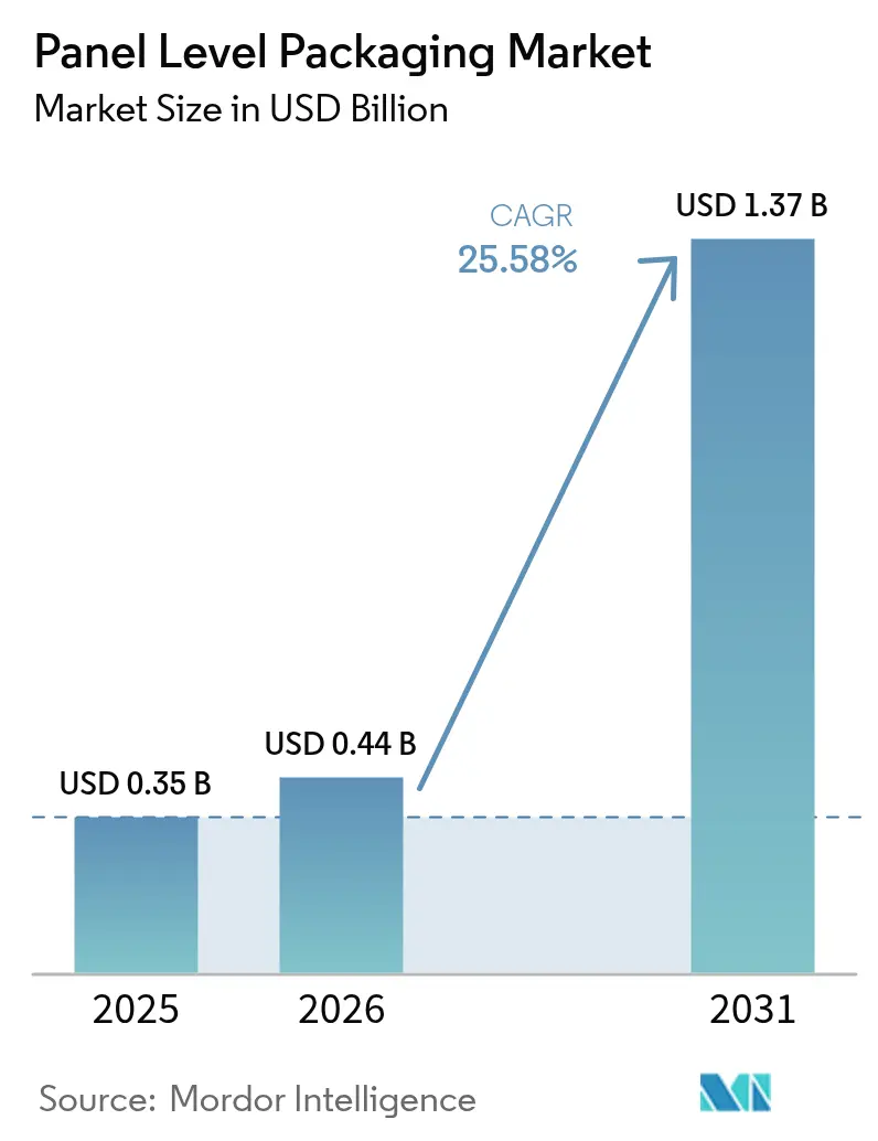
| Market Size (2026) | USD 0.44 Billion |
| Market Size (2031) | USD 1.37 Billion |
| Growth Rate (2026 - 2031) | 25.58% CAGR |
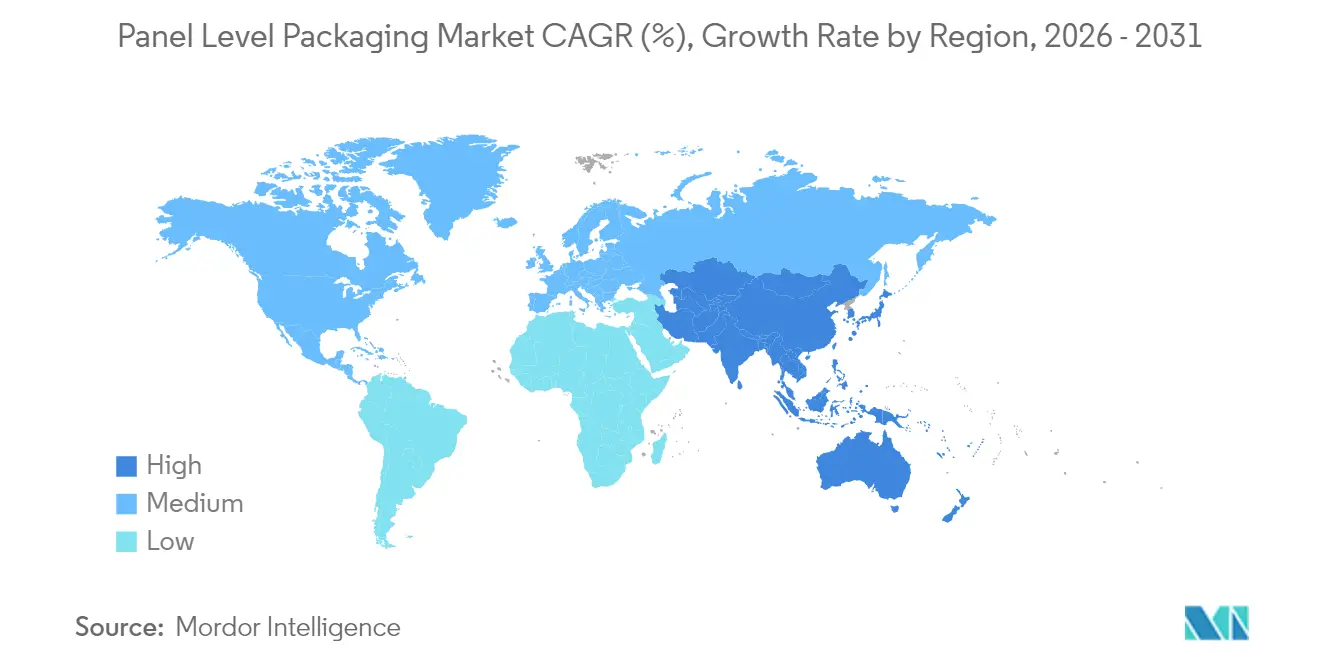
| Fastest Growing Market | Asia Pacific |
| Largest Market | Asia Pacific |
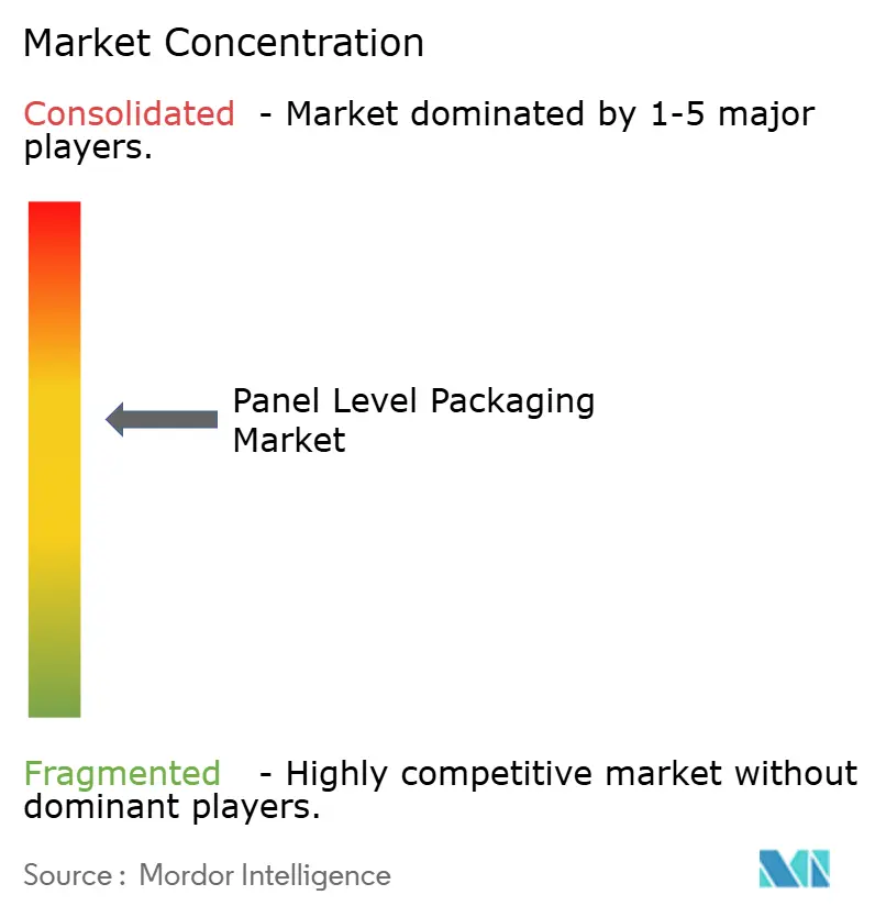
| Market Concentration | Medium |
Major Players *Disclaimer: Major Players sorted in no particular order Image © Mordor Intelligence. Reuse requires attribution under CC BY 4.0. | |
Panel Level Packaging Market Analysis by Mordor Intelligence
The panel-level packaging market size is expected to grow from USD 0.35 billion in 2025 to USD 0.44 billion in 2026 and is forecast to reach USD 1.37 billion by 2031 at 25.58% CAGR over 2026-2031. The steep trajectory mirrors the semiconductor sector’s shift from wafer-centric to panel-centric architectures, a move that unlocks scale advantages and aligns with burgeoning AI and high-performance computing demand. Panel formats deliver up to 40% better substrate utilization for multi-die designs, easing cost pressure as logic and memory nodes scale below 5 nm. Substrate innovation, notably the transition toward glass cores, promises tighter dimensional control and improved thermal stability, which together support rising input/output counts. Equipment vendors have responded with 600 mm × 600 mm lithography systems capable of sub-10 µm features, erasing a former resolution ceiling and widening the addressable market for next-generation integration. Supply-chain coordination is intensifying, illustrated by vertically integrated strategies from leading foundries and by cooperative capacity expansions between foundry and OSAT partners.
Key Report Takeaways
- By packaging technology, fan-out panel level packaging held 44.60% of the panel level packaging market share in 2025; 2.5D/3D panel integration is projected to grow at a 29.20% CAGR to 2031.
- By industry application, consumer electronics accounted for 40.30% of the panel-level packaging market size in 2025, while automotive ADAS and EV power applications are advancing at a 27.90% CAGR through 2031.
- By geography, Asia-Pacific captured 69.20% revenue share in 2025, and the region is set to expand at a 27.60% CAGR through 2031.
- By panel size, ≤300 mm × 300 mm commanded 58.90% of the panel level packaging market size in 2025, whereas panels ≥511 mm × 600 mm are forecast to post a 28.60% CAGR to 2031.
- By substrate material, Organic Laminate commanded 56.10% of the panel-level packaging market size in 2025, whereas Glass Core is forecast to post a 28.90% CAGR to 2031.
Note: Market size and forecast figures in this report are generated using Mordor Intelligence’s proprietary estimation framework, updated with the latest available data and insights as of 2026.
Global Panel Level Packaging Market Trends and Insights
Drivers Impact Analysis*
| Driver | (~) % Impact on CAGR Forecast | Geographic Relevance | Impact Timeline |
|---|---|---|---|
| Cost reduction versus wafer-level packaging | +4.2% | Global, APAC hubs | Medium term (2–4 years) |
| AI/HPC chip demand surge | +6.8% | North America, Asia-Pacific | Short term (≤2 years) |
| 5G/6G and edge-device proliferation | +5.1% | Global | Medium term (2–4 years) |
| Adoption of 600 mm × 600 mm digital lithography | +2.9% | Asia-Pacific, North America | Long term (≥4 years) |
| Transition to glass-core substrates ≥2026 | +3.7% | Taiwan, South Korea, U.S. | Long term (≥4 years) |
| EU/US reshoring subsidies for advanced packaging | +2.4% | North America, Europe | Medium term (2–4 years) |
| Source: Mordor Intelligence | |||


Cost Reduction Versus Wafer-Level Packaging
Moving to panel formats yields up to 40% better substrate utilization for multi-die designs, cutting cost per placement even after accounting for expensive tooling. ASE’s USD 200 million investment in 310 mm × 310 mm lines signals a commitment to volume scaling, and high-volume consumer devices supply the wafer starts needed to amortize tools across short life cycles. Asian contract manufacturers gain further leverage by clustering substrate fabrication, redistribution-layer processing, and final test inside single campuses, reducing logistics overhead. Western houses with lower volumes face a steeper cost curve, widening the competitiveness gap. As a result, panel-first strategies increasingly determine win rates in turnkey package bids[1]Norio Tanaka, “Fan-Out Panel Production Lines,” ASE Technology Holding, aseglobal.com .
Surge of AI/HPC Chip Demand
Large language-model inference and training floors require ever-denser GPU clusters, driving packaging toward larger interposer-free footprints that sustain bandwidth. TSMC’s Chip-on-Panel-on-Substrate (CoPoS) roadmap, slated for 2027 risk production, doubles reticle-limited dimensions of CoWoS while holding thermal resistance steady[2]T. Liu, “CoPoS Integration Strategy,” Taiwan Semiconductor Manufacturing Company, tsmc.com. The foundry is expanding CoWoS capacity more than 60% annually through 2026, yet still projects backlog in high-bandwidth memory (HBM) lines, pushing Tier-1 customers to evaluate panel-level packaging market alternatives for next-generation accelerator cards. Early movers able to demonstrate >20 kW shelf-level cooling in panel packages are best positioned to secure multi-year supply agreements.
Proliferation of 5G/6G and Edge Devices
Emerging radios integrate mm-wave front-ends with digital baseband and power-management units on shared substrates. Panel architectures better dissipate localized hotspots while supporting the ultra-tight pitch needed for co-packaged optics. For edge servers, designers embrace heterogeneous die layouts that fuse low-power AI cores with memory and SerDes in space-constrained enclosures; panel fan-out improves thermal spread and signal integrity, boosting field reliability when deployed in industrial or outdoor settings.
Nikon 600 × 600 mm digital lithography adoption
The DSP-100 tool brings maskless digital lithography to full 600 mm × 600 mm substrates, printing sub-10 µm lines while trimming cycle time versus step-and-repeat scanners[3]Nikon 600 × 600 mm digital lithography adoption Nikon 600 × 600 mm digital lithography adoption . OSATs that install first-wave systems gain the capacity to fabricate ultra-high-I/O redistribution layers in a single shot, removing stitch errors that plagued earlier panel experiments. Capital outlay remains heavy, topping USD 80 million per chamber, and only top-tier packaging houses with AI-grade order books can clear hurdle rates. Nevertheless, pilot yields above 95% after three months of ramp point to a durable learning curve advantage for adopters.
Restraints Impact Analysis*
| Restraint | (~) % Impact on CAGR Forecast | Geographic Relevance | Impact Timeline |
|---|---|---|---|
| High capital intensity and warpage issues | -3.1% | Global, small OSATs | Short term (≤2 years) |
| Process-integration complexity beyond 300 mm | -2.8% | Asia-Pacific, Global | Medium term (2–4 years) |
| Sub-1 µm lithography yield cliff on large panels | -2.4% | Advanced foundries | Medium term (2–4 years) |
| ABF-GCP dielectric film bottleneck | -1.9% | High-volume fabs | Short term (≤2 years) |
| Source: Mordor Intelligence | |||
High Capital Intensity and Warpage Issues
A full 600 mm line demands more than USD 500 million in deposition, patterning, and metrology gear. Panel substrates expand under thermal load, generating a bow that can exceed 2 mm if not compensated. SK Key Foundry and LB Semicon’s Direct-RDL flow clamps panel edges during cure to limit deflection, but equipment retrofits add 15% to tool cost.[4]Dr. Y. C. Kim, “Direct-RDL for Automotive,” SK Key Foundry, skkeyfoundry.com Smaller OSATs struggle to finance those upgrades, constraining global supply expansion. Until low-modulus dielectrics or active warp-compensation chucks mature, yield drag remains a check on near-term penetration of the panel-level packaging market.
Process-Integration Complexity Beyond 300 mm
Uniformity windows tighten sharply as panels grow. Temperature gradients as small as 2 °C can skew copper thickness by 8%, driving impedance drift. Tool vendors now pair multi-zone heaters with laser-based thickness monitors, but recipe qualification stretches over quarters rather than weeks. Firms with deep process-engineering benches can tune dozens of parameters in parallel; second-tier players must accept lower throughput or outsource early learning to equipment partners, blunting margins. The result is a steep capability hierarchy that hinders ecosystem diversity and slows the diffusion rate of panel-level packaging industry know-how.
*Our forecasts treat driver/restraint impacts as directional, not additive. The impact forecasts reflect baseline growth, mix effects, and variable interactions.
Segment Analysis
By Packaging Technology: Balancing Fan-Out Scale and 3D Bandwidth
Fan-Out Panel Level Packaging commanded 44.60% of 2025 revenue, making it the workhorse for consumer and mobile devices where moderate I/O density is sufficient. The panel-level packaging market size for this segment reached USD 0.16 billion and is projected to grow at 19.80% through 2031. Large OSATs leverage mature die-face-down flows to drive yields above 97%, beating wafer fan-out costs by double-digit margins on runs above 20,000 panels per month. Nevertheless, bandwidth-hungry accelerators are stretching the approach’s pad pitch limits, pressing innovators toward 2.5D/3D panel solutions.
2.5D/3D panel integration, while holding only 19.10% of 2025 sales, is the fastest mover at a 29.20% CAGR. Heterogeneous stacking places compute, memory, and analog tiles on passive glass carriers, cutting interconnect length by up to 70%. Early commercial wins center on AI inference cards where a single package hosts >16 chiplets. The panel-level packaging market share for 2.5D/3D approaches is expected to hit 31.80% by 2031 as the technique escapes datacenter niches and filters into automotive domain controllers.


By Substrate Material: Organic Leadership Faces Glass Momentum
Organic laminate retained a 56.10% share in 2025, valued at USD 0.20 billion, benefiting from low-cost resin systems and entrenched supply chains. However, the segment’s 20.40% CAGR lags the overall panel-level packaging market, reflecting physical limits on layer count and CTE mismatch. Glass cores, in contrast, posted only an 12.30% share last year but will grow at a 28.90% CAGR to 2031. Samsung’s H-glass roadmap targets volume ramp in 2026, offering 0.3 ppm/°C dimensional drift, one-tenth that of organics, unlocking sub-5 µm line-width redistribution layers. Silicon and molded reconstituted panels remain niche, serving high-power or ultra-low-cost corners.
By Panel Size: Small-Format Maturity Meets Large-Panel Upside
Panels ≤300 mm × 300 mm account for 58.90% of revenue yet trail in growth at 18.60% CAGR. The widely available 320 mm exposure tools and standard pick-and-place heads favor this footprint for smartphones and wearables. The panel-level packaging market size for large-format ≥511 mm × 600 mm panels, though minor today, is climbing 28.60% annually as HPC firms chase more dies per substrate. Nikon’s DSP-100 removes lithography bottlenecks, while new laser-dicing systems keep singulation yield above 99% even on 600 mm glass.

By Industry Application: Consumer Base Anchors, Automotive Gains Velocity
Consumer electronics led with a 40.30% share in 2025, translating to USD 0.14 billion. Smartphones, tablets, and AR headsets adopt a fan-out panel to shave the motherboard area and thickness. The automotive slice, covering ADAS radars and SiC power modules, is on course for a 27.90% CAGR as OEMs electrify fleets and demand 15-year reliability. Telecommunications infrastructure holds a mid-teens share, buoyed by massive MIMO radios that require integrated RF-digital modules. Aerospace, defense, industrial, and IoT applications together occupy the remainder, each valuing specific thermal or ruggedization benefits.
Geography Analysis
Asia-Pacific captured 69.20% of 2025 revenue and continues to lead the panel-level packaging market at a 27.60% CAGR through 2031. China funnels state incentives toward panel packaging lines aligned with sovereign AI chip programs, and Japan’s equipment outlays rose 82% in 2024 to USD 7 billion, underpinning domestic process capability. South Korea advances glass-core substrates, while Taiwan’s TSMC pushes integrated foundry-packaging flows that bundle CoWoS, CoPoS, and testing in a single fab cluster.
North America follows, anchored by CHIPS-Act funding of USD 1.6 billion earmarked for advanced packaging. Amkor’s USD 400 million Arizona plant comes online in 2026, co-located with TSMC’s new Fab 21 to shorten cycle times for U.S. customers. SK Hynix likewise has earmarked USD 450 million for HBM packaging in Indiana, demonstrating that states are bidding aggressively for high-value backend operations.
Europe’s share remains single-digit but is rising as sovereignty concerns spur local OSAT formation. Foxconn and Thales committed EUR 250 million to a new fan-out facility aimed at aerospace and defense, while Infineon partnered with Amkor to add panel capacity in Portugal that comes online mid-2025. Middle East and Africa and South America remain consumption-centric, with limited assembly footprints yet, though incentive schemes in Saudi Arabia and Brazil could shift that balance later in the decade.

Competitive Landscape
Competition is intensifying as foundries integrate downstream processes and OSATs move upstream. TSMC’s Wafer Manufacturing 2.0 program unites lithography, packaging, and final test under a single scheduling system to shave weeks off delivery windows. Samsung counters via internal glass-substrate production to secure a materials moat, while Intel applies its embedded multi-die interconnect bridge (EMIB) to compete on system-level performance.
Equipment vendors carve out defensible niches: Applied Materials leads in copper-barrier deposition for 1 µm redistribution layers, whereas Tokyo Electron ships spin-on dielectric coaters optimized for low-warpage glass. Nikon’s first-mover maskless lithography expands its influence beyond wafer fabs into the panel-level packaging industry. Vertical tie-ups are growing: ASE’s strategic alignment with TSMC on 310 mm panels pools capex to accelerate learning curves, foreshadowing more collaborative megaprojects.
White-space opportunities persist in ultra-reliable sectors. Micro-System Engineering exploits its medical-device pedigree to deliver hermetic ceramic-glass hybrids, and Micross has bolstered defense offerings via strategic acquisitions. Nonetheless, high capex thresholds deter greenfield entrants, setting the stage for gradual consolidation once initial demand spikes normalize.
Panel Level Packaging Industry Leaders
ASE Technology Holding Co., Ltd.
Taiwan Semiconductor Manufacturing Company Limited (TSMC)
Samsung Electronics Co., Ltd.
Amkor Technology, Inc.
Intel Corporation
- *Disclaimer: Major Players sorted in no particular order

Recent Industry Developments
- July 2025: Nikon released the DSP-100 direct-write lithography platform for 600 mm × 600 mm panels, delivering sub-10 µm resolution and enabling high-I/O fan-out packages.
- July 2025: SK Key Foundry and LB Semicon completed development of warpage-mitigating “Direct RDL” technology aimed at automotive semiconductor reliability standards.
- June 2025: TSMC and ASE Holdings agreed to co-develop a 310 mm × 310 mm panel flow, aligning layouts with forthcoming AI accelerators that outgrow wafer reticles.
- May 2025: Foxconn and Thales committed EUR 250 million to a European OSAT plant employing fan-out technology for defense and space applications.


Global Panel Level Packaging Market Report Scope
Panel-level packaging is one of the following steps for fan-out wafer-level packaging. Vendors worldwide are focusing on upscaling PLP instead of drawing a roadmap to 450 mm fan-out wafer-level packaging. PLP is expected to offer significant cost advantages by parallelizing process steps and allowing higher area utilization of packages in rectangular panel formats rather than round wafer shapes to lower material waste.
The panel level packaging market is segmented by industry application (consumer electronics, automotive, telecommunication, and other industry applications) and geography (United States, China, Korea, Taiwan, Japan, Europe, Rest of the World). The report offers the market size in value terms in USD for all the abovementioned segments.
| Fan-Out Panel Level Packaging (FOPLP) |
| Embedded Bridge (eBridge) |
| 2.5D/3D Panel Integration |
| Fan-In Panel Level Packaging |
| Organic Laminate |
| Glass Core |
| Silicon |
| Molded Reconstituted Panel |
| ≤300 mm × 300 mm |
| 301 – 510 mm × 510 mm |
| ≥511 mm × 600 mm |
| Consumer Electronics |
| Automotive (ADAS, EV Power) |
| Telecommunications (5G/6G Infrastructure) |
| Aerospace and Defense |
| Industrial and IoT |
| North America | United States |
| Canada | |
| Mexico | |
| South America | Brazil |
| Argentina | |
| Rest of South America | |
| Europe | Germany |
| United Kingdom | |
| France | |
| Italy | |
| Rest of Europe | |
| Asia-Pacific | China |
| Japan | |
| South Korea | |
| India | |
| Rest of Asia-Pacific | |
| Middle East | Saudi Arabia |
| United Arab Emirates | |
| Rest of Middle East | |
| Africa | South Africa |
| Rest of Africa |
| By Packaging Technology | Fan-Out Panel Level Packaging (FOPLP) | |
| Embedded Bridge (eBridge) | ||
| 2.5D/3D Panel Integration | ||
| Fan-In Panel Level Packaging | ||
| By Substrate Material | Organic Laminate | |
| Glass Core | ||
| Silicon | ||
| Molded Reconstituted Panel | ||
| By Panel Size | ≤300 mm × 300 mm | |
| 301 – 510 mm × 510 mm | ||
| ≥511 mm × 600 mm | ||
| By Industry Application | Consumer Electronics | |
| Automotive (ADAS, EV Power) | ||
| Telecommunications (5G/6G Infrastructure) | ||
| Aerospace and Defense | ||
| Industrial and IoT | ||
| By Geography | North America | United States |
| Canada | ||
| Mexico | ||
| South America | Brazil | |
| Argentina | ||
| Rest of South America | ||
| Europe | Germany | |
| United Kingdom | ||
| France | ||
| Italy | ||
| Rest of Europe | ||
| Asia-Pacific | China | |
| Japan | ||
| South Korea | ||
| India | ||
| Rest of Asia-Pacific | ||
| Middle East | Saudi Arabia | |
| United Arab Emirates | ||
| Rest of Middle East | ||
| Africa | South Africa | |
| Rest of Africa | ||


Key Questions Answered in the Report
How fast is the panel level packaging market expected to grow to 2031?
It is forecast to post a 25.58% CAGR, rising from USD 0.35 billion in 2025 to USD 1.37 billion by 2031.
Which region leads panel level packaging revenue today?
Asia-Pacific holds 69.20% of 2025 revenue and remains the fastest-expanding area through 2031.
What application segment shows the highest future growth?
Automotive ADAS and EV power modules are projected to advance at a 27.90% CAGR to 2031.
Why are glass substrates gaining attention in packaging?
Glass cores offer superior dimensional stability and lower dielectric loss, enabling tighter routing for AI and 6G devices.
What is the biggest technical hurdle for very-large panels?
Warpage control and sub-micron lithography yield cliffs present the main manufacturing challenges above 300 mm formats.
How will U.S. CHIPS Act funding influence the sector?
Federal incentives accelerate domestic panel capacity, tightening supply resilience for North American defense and cloud customers.
Page last updated on:


