High-End Semiconductor Packaging Market Size and Share
Market Overview
| Study Period | 2020 - 2031 |
|---|---|
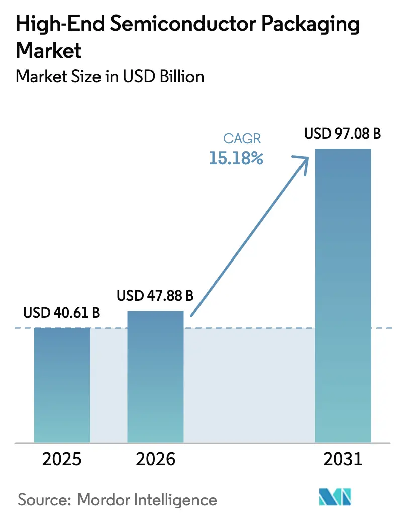
| Market Size (2026) | USD 47.88 Billion |
| Market Size (2031) | USD 97.08 Billion |
| Growth Rate (2026 - 2031) | 15.18% CAGR |
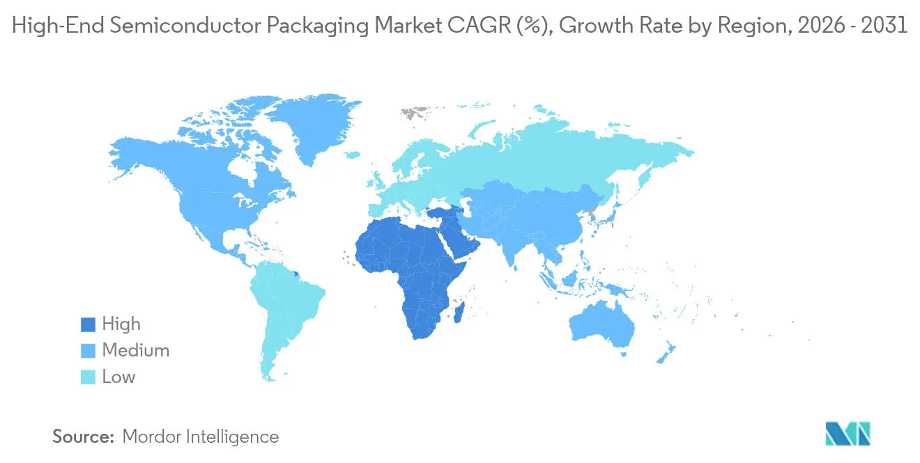
| Fastest Growing Market | Middle East |
| Largest Market | Asia Pacific |
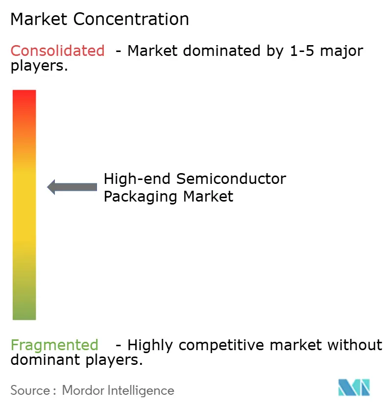
| Market Concentration | Medium |
Major Players *Disclaimer: Major Players sorted in no particular order Image © Mordor Intelligence. Reuse requires attribution under CC BY 4.0. | |
High-End Semiconductor Packaging Market Analysis by Mordor Intelligence
The high-end semiconductor packaging market size is expected to increase from USD 40.61 billion in 2025 to USD 47.88 billion in 2026 and reach USD 97.08 billion by 2031, growing at a CAGR of 15.18% over 2026-2031. Surging artificial-intelligence workloads are lifting demand for high-bandwidth memory stacks that rely on through-silicon vias, while smartphone original-equipment manufacturers have shifted flagship application processors to 3-nanometer nodes that require advanced flip-chip and fan-out architectures. Data-center operators are pre-ordering HBM3E supply eighteen months in advance, prompting memory makers to re-tool DRAM lines for vertically stacked products. Panel-level processes on glass substrates promise scale economies, yet yield challenges constrain near-term adoption and sustain flip-chip leadership. Investment intensity above USD 500 million per line is concentrating capacity among a handful of outsourced semiconductor assembly and test providers and vertically integrated foundries.
Key Report Takeaways
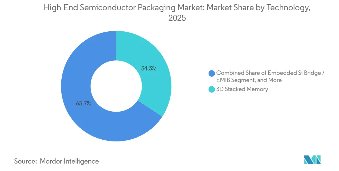
- By technology, 3D stacked memory led with 34.28% revenue share in 2025, while embedded silicon bridge architectures are projected to expand at a 16.01% CAGR through 2031.
- By packaging platform, flip-chip BGA captured 38.53% of 2025 revenue, whereas panel-level packaging is the fastest growing platform at a 16.16% CAGR to 2031.
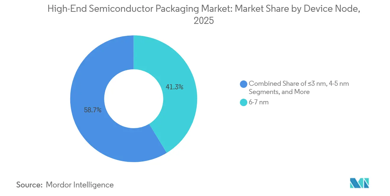
- By device node, the 6-7 nanometer segment held 41.27% of 2025 revenue, but sub-3 nanometer devices are advancing at a 15.97% CAGR over the forecast period.
- By end user, consumer electronics accounted for 29.81% of 2025 revenue, and automotive and ADAS applications are forecast to grow at a 15.91% CAGR through 2031.
- By geography, Asia-Pacific generated 53.73% of 2025 revenue, while the Middle East is set to expand at a 15.89% CAGR to 2031.
Note: Market size and forecast figures in this report are generated using Mordor Intelligence’s proprietary estimation framework, updated with the latest available data and insights as of 2026.
Global High-End Semiconductor Packaging Market Trends and Insights
Driver Impact Analysis*
| Driver | (~) % Impact on CAGR Forecast | Geographic Relevance | Impact Timeline |
|---|---|---|---|
| Rising Demand for AI/ML Accelerators | +3.20% | Global, with concentration in North America and Asia-Pacific | Medium term (2-4 years) |
| Demand Spike from Data-Center HBM3E Roll-Outs | +2.80% | North America, Asia-Pacific | Short term (≤ 2 years) |
| Smartphone Migration to Advanced Nodes | +2.40% | Asia-Pacific, spillover to Europe and North America | Medium term (2-4 years) |
| Thermal-Embedded Interposers Improving Yield at ≤3 nm | +2.10% | Asia-Pacific core, expanding to North America | Long term (≥ 4 years) |
| Adoption of Chiplets for LEO Satellite Payloads | +1.60% | North America, Europe | Long term (≥ 4 years) |
| Government-Funded More-than-Moore Pilot Lines in Europe | +1.40% | Europe, with technology transfer to Middle East | Long term (≥ 4 years) |
| Source: Mordor Intelligence | |||
Rising Demand For AI/ML Accelerators
Hyperscale operators deployed more than 2 million AI accelerators in 2025, each integrating four to eight HBM3E stacks that depend on 3D through-silicon-via bonding, converting what was a niche configuration into a mainstream requirement for the high-end semiconductor packaging market.[1]ASE invested USD 1.2 billion in a fan-out facility in Penang, Malaysia, set to open in 2027. Memory vendors introduced 12-layer devices delivering over 1 terabyte-per-second bandwidth, a milestone unattainable with planar DRAM interfaces.[2]Samsung Electronics, “Samsung Electronics Begins Mass Production of Industry's First 12-Layer HBM3E,” news.samsung.com Edge-AI inference is creating secondary demand for lower-power HBM variants, broadening addressable volume beyond cloud servers. The driver carries medium-term weight because model sizes continue to rise and data-sovereignty regulation favours on-premises acceleration. Packaging houses that can meet micro-bump pitches below 40 µm are best placed to capture this growth.
Demand Spike from Datacenter HBM3E Rollouts
Data-center capital expenditure climbed to USD 250 billion in 2025, with AI-optimized servers representing 38% of unit shipments, up from 22% in 2024.[3]Financial Times, “Data Center Capex AI Servers 2025,” ft.com Memory makers diverted half of total DRAM capacity to HBM fabrication, signalling structural reallocation away from commodity products. Single-socket systems, each fed by multi-terabyte-per-second HBM3E, have replaced multi-node clusters for inference, compressing rack counts and elevating package-level thermal density. Short-term impact is high because hyperscalers secure allocations 12-18 months ahead, locking in demand visibility for advanced packaging lines.
Smartphone Migration to Advanced Nodes
Apple’s A18 and Qualcomm’s Snapdragon 8 Gen 4 were taped out on 3-nanometer nodes in 2025, pushing localized heat flux above 200 W/cm², which necessitates flip-chip BGA packages with integrated heat spreaders. The packaging bill-of-materials per flagship handset doubled to USD 12, yet brands accept the premium to unlock on-device generative-AI features. Mid-tier devices are now migrating to 4-5 nanometer nodes, trickling advanced packaging demand into higher-volume price bands. Asia-Pacific remains the primary production hub, but thermal-performance requirements are driving collaborative development between material suppliers in Europe and design houses in North America.
Thermal-Embedded Interposers Improving Yield At ≤3 nm
Pilot data from IMEC shows micro-channel-cooled interposers raise parametric yield by 8-12 percentage points at 3 nanometer logic densities. Intel’s EMIB-T integrates thermal and electrical vias, cutting junction temperature by 15 °C during sustained workloads. Automotive Tier-1 suppliers demand these solutions to meet AEC-Q100 Grade 1 temperature windows, yet qualification cycles of 24-36 months mean volume revenue arrives later, giving this driver a long-term profile.
Restraints Impact Analysis*
| Restraint | (~) % Impact on CAGR Forecast | Geographic Relevance | Impact Timeline |
|---|---|---|---|
| Escalating Capital Intensity | -2.50% | Global, acute in Europe and North America | Medium term (2-4 years) |
| Substrate Supply Bottlenecks for Organic Interposers | -2.20% | Asia-Pacific, spillover to North America | Short term (≤ 2 years) |
| Yield-Management Complexity Beyond 5 nm | -1.80% | Asia-Pacific core, expanding to North America | Long term (≥ 4 years) |
| Non-Uniform Thermal Dissipation in 3D-SoC Stacks | -1.30% | Global, critical for automotive and aerospace | Long term (≥ 4 years) |
| Source: Mordor Intelligence | |||
Escalating Capital Intensity
Hybrid-bonding, laser debonding and sub-micron metrology tools lift panel-level line costs beyond USD 500 million, three times higher than legacy flip-chip tooling. Amkor’s USD 2 billion Arizona project illustrates the scale barriers for mid-tier entrants. Equipment lead times of up to 18 months force early volume commitments that heighten financial risk, especially in Europe and North America where subsidies cover only a quarter of project outlays.
Substrate Supply Bottlenecks for Organic Interposers
Lead times for Ajinomoto Build-up Film substrates stretched to 26 weeks in late 2025, double the prior year, after capacity expansion lagged AI-accelerator demand. Unimicron and Ibiden plan a combined 15% capacity lift by 2026, but output will not reach economic yield until late 2027. Tight supply elevates allocation risk for North American fabless firms and can delay revenue from early-adopter product launches.
*Our forecasts treat driver/restraint impacts as directional, not additive. The impact forecasts reflect baseline growth, mix effects, and variable interactions.
Segment Analysis
By Technology: Memory Stacks Drive Revenue, Bridges Capture Margin
3D stacked memory held the largest share of 2025 revenue, a position sustained by HBM adoption in AI accelerators that require vertical DRAM integration to exceed 1 TB/s per stack. Embedded silicon bridge solutions are forecast to outpace all other technologies at a 16.01% growth rate as Universal Chiplet Interconnect Express enables sub-10 ns latency between heterogeneous dies.
The high-end semiconductor packaging market rewards bridge architectures with premium pricing because they replace costly full-interposer designs and offer better thermal paths. Low-earth-orbit satellite operators value chiplet modularity because individual tiles can be swapped without retiring entire payload modules, keeping lifecycle costs in check. Compliance with the JEDEC HBM3 standard increases vendor interchangeability, nudging margin capture toward packaging houses that can guarantee high-reliability micro-bump formations.


By Packaging Platform: Flip-Chip Dominates, Panels Promise Scale
Flip-chip BGA controlled 38.53% of platform revenue in 2025, underlining its entrenched role in high-performance computing, networking and automotive domains where electrical parasitic must be minimal. Panel-level packaging is projected to post the fastest growth at 16.16% because larger glass panels dilute lithography costs, yet warpage during reflow has prevented large-scale migration of high-pin-count devices.
Automotive qualification cycles remain a gating factor; no panel-level package has yet completed 1 000-hour high-temperature operating life at −40 °C to 150 °C, prolonging flip-chip dominance. The high-end semiconductor packaging market size for panel-level solutions will expand as substrate suppliers refine glass-core dimensional stability, but a decisive shift requires die-attach yields above 98%, a level still elusive in 2026 trials.
By Device Node: Sub-3 nm Adoption Accelerates
Devices fabricated on 6-7 nanometer processes accounted for 41.27% of 2025 revenue, but sub-3 nanometer products are forecast to post the highest 15.97% growth as smartphone processors and AI accelerators push for power efficiency. Thermal-embedded interposers are essential at these geometries because power density exceeds 150 W/cm², challenging conventional heat-sink solutions.
Known-good-die testing adds 15-20% to production cost at sub-5-nanometer nodes, yet customers accept the premium to secure the performance edge. Export controls on extreme-ultraviolet lithography tools restrict regional capacity additions, indirectly tightening the supply of advanced packaging services tied to leading-edge nodes.
By End User: Automotive Gains Share
Consumer electronics generated 29.81% of 2025 revenue, but growth is moderating as refresh cycles lengthen and differentiation shifts toward software features. Automotive and ADAS demand is rising at a 15.91% CAGR, with each Level 3 autonomous vehicle embedding 8-12 high-performance SoCs that require thermally optimized system-in-package modules.
Telecom infrastructure is stabilizing after the first wave of 5G base-station roll-outs, yet Open RAN adoption spurs demand for modular chiplet designs. Aerospace and defense users pay premium pricing for hermetic and radiation-hardened packages that comply with MIL-STD-883, but volumes remain niche.
Geography Analysis
Asia-Pacific captured 53.73% of 2025 market revenue, buoyed by Taiwan Semiconductor Manufacturing Company’s planned 60% CoWoS capacity expansion and South Korea’s 90% share of global HBM3E supply. China’s JCET and Tongfu Microelectronics scaled fan-out lines to serve domestic fabless firms despite export-control constraints on leading-edge equipment.
The Middle East is the fastest-growing region, projected at a 15.89% CAGR as the United Arab Emirates and Saudi Arabia deploy sovereign wealth to attract back-end assembly projects; the EUR 43 billion (USD 46.4 billion) European Chips Act model is guiding subsidy design. North America accounts for roughly 18% of revenue, anchored by CHIPS Act-backed plants in Arizona and Texas.
Europe holds 8% of the market, limited by higher labour costs, but pilot lines at IMEC and Fraunhofer are advancing More-than-Moore interposer concepts, with rollout contingent on long-term offtake deals. South America and Africa together remain below 2%, importing most advanced-packaged devices and lacking substrate supply chains.

Competitive Landscape
The top five outsourced semiconductor assembly and test companies ASE, Amkor Technology, JCET Group, Siliconware Precision Industries and Powertech Technology control about 60% of global advanced-packaging capacity, giving the high-end semiconductor packaging market a moderate concentration profile. Taiwan Semiconductor Manufacturing Company is blurring front-end and back-end boundaries by internalizing CoWoS and system-on-wafer services, offering single-vendor accountability for yield.
Intel and Samsung are piloting glass-core substrates that promise lower loss and finer linewidths than organic interposers, but tooling costs above USD 100 million per line limit near-term adoption. Substrate makers such as Unimicron are forward integrating into assembly to leverage control over Ajinomoto Build-up Film allocation, thereby securing long-term contracts with fabless firms facing supply uncertainty.
Hybrid-bonding platforms like Intel’s Foveros and Taiwan Semiconductor Manufacturing Company’s SoIC achieve sub-10 µm pitches and are becoming default choices for AI accelerators. Patent filings in thermal-via integration grew 34% year-over-year in 2025, signalling industry emphasis on heat-management innovation.
High-End Semiconductor Packaging Industry Leaders
Intel Corporation
Taiwan Semiconductor Manufacturing Company
Advanced Semiconductor Engineering, Inc
Samsung Electronics Co. Ltd
Amkor Technology Inc.
- *Disclaimer: Major Players sorted in no particular order

Recent Industry Developments
- February 2026: Taiwan Semiconductor Manufacturing Company committed USD 5 billion to enlarge CoWoS capacity by 60% for AI accelerator demand.
- January 2026: SK Hynix ramped 16-layer HBM4 with 1.5 TB/s bandwidth and 48 GB capacity.
- December 2025: Intel announced EMIB-T packaging will be offered as a foundry service from Q3 2026.
- November 2025: ASE invested USD 1.2 billion in a fan-out facility in Penang, Malaysia, set to open in 2027.


Global High-End Semiconductor Packaging Market Report Scope
The High-End Semiconductor Packaging Market Report is Segmented by Technology (3D System-on-Chip, 3D Stacked Memory, 2.5D Interposers, Ultra-High-Density Fan-Out, Embedded Si Bridge), Packaging Platform (Flip-Chip BGA, WLCSP, Panel-Level Packaging, System-in-Package), Device Node (≤3 nm, 4-5 nm, 6-7 nm, ≥10 nm), End User (Consumer Electronics, Telecom and 5G, Automotive and ADAS, Aerospace and Defense, Medical Devices), and Geography (North America, South America, Europe, Asia-Pacific, Middle East and Africa). Market Forecasts are Provided in Terms of Value (USD).
| 3D System-on-Chip (3D-SoC) |
| 3D Stacked Memory (HBM, HBM-PIM) |
| 2.5D Interposers |
| Ultra-High-Density Fan-Out (UHD-FO) |
| Embedded Si Bridge / EMIB |
| Flip-Chip Ball-Grid-Array (FC-BGA) |
| Wafer-Level Chip-Scale Package (WLCSP) |
| Panel-Level Packaging (PLP) |
| System-in-Package (SiP) |
| Less than 3 nm |
| 4-5 nm |
| 6-7 nm |
| More than equal to 10 nm |
| Consumer Electronics |
| Telecom and 5G Infrastructure |
| Automotive and ADAS |
| Aerospace and Defense |
| Medical Devices |
| North America | United States | |
| Canada | ||
| Mexico | ||
| South America | Brazil | |
| Argentina | ||
| Colombia | ||
| Rest of South America | ||
| Europe | United Kingdom | |
| Germany | ||
| France | ||
| Italy | ||
| Spain | ||
| Rest of Europe | ||
| Asia-Pacific | China | |
| Japan | ||
| South Korea | ||
| India | ||
| Rest of Asia-Pacific | ||
| Middle East and Africa | Middle East | Saudi Arabia |
| United Arab Emirates | ||
| Rest of Middle East | ||
| Africa | South Africa | |
| Egypt | ||
| Rest of Africa | ||
| By Technology | 3D System-on-Chip (3D-SoC) | ||
| 3D Stacked Memory (HBM, HBM-PIM) | |||
| 2.5D Interposers | |||
| Ultra-High-Density Fan-Out (UHD-FO) | |||
| Embedded Si Bridge / EMIB | |||
| By Packaging Platform | Flip-Chip Ball-Grid-Array (FC-BGA) | ||
| Wafer-Level Chip-Scale Package (WLCSP) | |||
| Panel-Level Packaging (PLP) | |||
| System-in-Package (SiP) | |||
| By Device Node | Less than 3 nm | ||
| 4-5 nm | |||
| 6-7 nm | |||
| More than equal to 10 nm | |||
| By End User | Consumer Electronics | ||
| Telecom and 5G Infrastructure | |||
| Automotive and ADAS | |||
| Aerospace and Defense | |||
| Medical Devices | |||
| By Geography | North America | United States | |
| Canada | |||
| Mexico | |||
| South America | Brazil | ||
| Argentina | |||
| Colombia | |||
| Rest of South America | |||
| Europe | United Kingdom | ||
| Germany | |||
| France | |||
| Italy | |||
| Spain | |||
| Rest of Europe | |||
| Asia-Pacific | China | ||
| Japan | |||
| South Korea | |||
| India | |||
| Rest of Asia-Pacific | |||
| Middle East and Africa | Middle East | Saudi Arabia | |
| United Arab Emirates | |||
| Rest of Middle East | |||
| Africa | South Africa | ||
| Egypt | |||
| Rest of Africa | |||


Key Questions Answered in the Report
What is the projected size of high-end semiconductor packaging by 2031?
The segment is forecast to reach USD 97.08 billion in 2031, up from USD 47.88 billion in 2026.
Which technology segment is set to expand the fastest?
Embedded silicon bridge architectures are projected to post the highest growth, advancing at a 16.01% CAGR through 2031.
How rapidly are panel-level packaging revenues expected to rise?
Panel-level solutions are on track for a 16.16% compound annual growth rate between 2026 and 2031.
Why are AI data centers fueling demand for high-bandwidth memory packages?
Each accelerator server now integrates multiple HBM3E stacks to achieve terabyte-per-second bandwidth, a configuration only possible with advanced 3D packaging.
Which geography is anticipated to record the quickest revenue growth?
The Middle East is expected to register the fastest pace, with a 15.89% CAGR projected through 2031.
What factors still limit panel-level adoption in automotive electronics?
Yield challenges from panel warpage and the need to complete AEC-Q100 reliability testing keep most vehicle programs on established flip-chip platforms for now.
Page last updated on:


