System In Package (SIP) Die Market Size and Share
Market Overview
| Study Period | 2020 - 2031 |
|---|---|
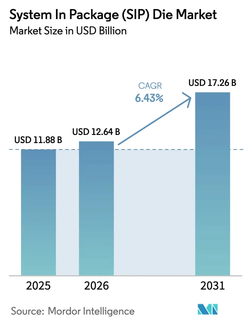
| Market Size (2026) | USD 12.64 Billion |
| Market Size (2031) | USD 17.26 Billion |
| Growth Rate (2026 - 2031) | 6.43% CAGR |
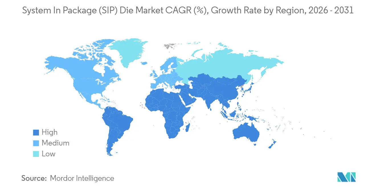
| Fastest Growing Market | South America |
| Largest Market | North America |
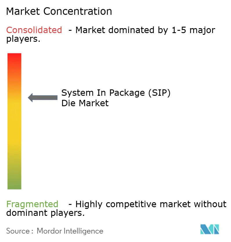
| Market Concentration | Medium |
Major Players *Disclaimer: Major Players sorted in no particular order Image © Mordor Intelligence. Reuse requires attribution under CC BY 4.0. | |
System In Package (SIP) Die Market Analysis by Mordor Intelligence
The System-in-Package die market size is expected to grow from USD 11.88 billion in 2025 to USD 12.64 billion in 2026 and is forecast to reach USD 17.26 billion by 2031 at 6.43% CAGR over 2026-2031. The expansion stems from rapid heterogeneous integration that lets designers combine logic, memory, photonics, and power devices inside one enclosure to meet artificial intelligence, 5G infrastructure, and vehicle electrification workloads. Robust demand for advanced chiplets, larger fan-out formats, and automotive-grade thermal solutions underpins a steady upgrade cycle across foundries, outsourced-semiconductor-assembly-and-test (OSAT) providers, and original-equipment manufacturers. Strategic government incentives in the United States, the European Union, and Japan are widening domestic capacity, while Asia-Pacific incumbents scale panel-level lines to maintain cost leadership. Supply-chain resilience, substrate innovation, and co-packaged optics prototypes further reinforce the long-term outlook for the System-in-Package die market. [1]TSMC, “2025 Capital Budget Highlights,” tsmc.com
Key Report Takeaways
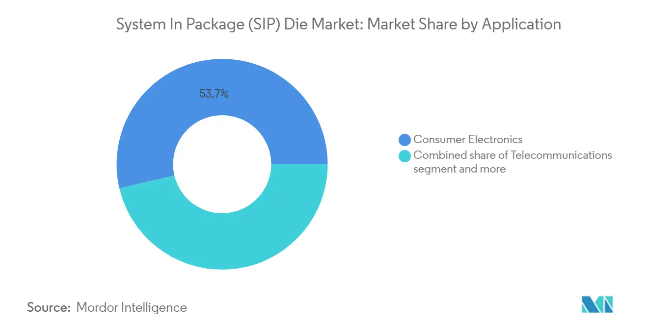
- By application, consumer electronics led with 53.68% of System-in-Package die market share in 2025; automotive is projected to grow at an 11.42% CAGR to 2031.
- By material type, silicon substrates commanded 84.35% share of the System-in-Package die market size in 2025, whereas glass substrates are set to expand at a 9.78% CAGR through 2031.
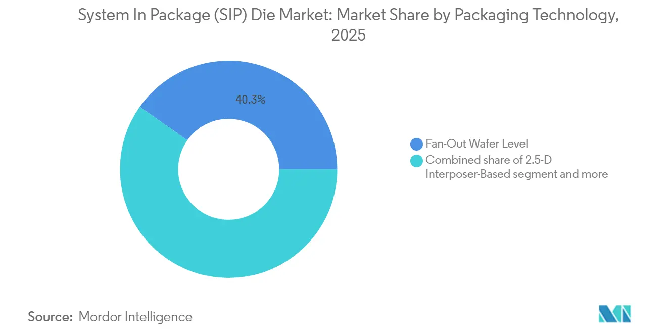
- By packaging technology, fan-out wafer-level packaging held 40.25% revenue share in 2025; fan-out panel-level packaging is the fastest-growing technology at a 12.05% CAGR to 2031.
- By end-use device, smartphones accounted for 46.10% of System-in-Package die market size in 2025, while wearables are advancing at a 14.08% CAGR through 2031.
- Asia-Pacific captured 62.10% of global revenue in 2025, reflecting dominant manufacturing ecosystems and multi-billion-dollar capital-expenditure programs.
Note: Market size and forecast figures in this report are generated using Mordor Intelligence’s proprietary estimation framework, updated with the latest available data and insights as of 2026.
Global System In Package (SIP) Die Market Trends and Insights
Drivers Impact Analysis*
| Driver | (~) % Impact on CAGR Forecast | Geographic Relevance | Impact Timeline |
|---|---|---|---|
| Advanced semiconductor node adoption (≤7 nm) | 1.80% | Global, concentrated in Taiwan, South Korea | Medium term (2-4 years) |
| Expansion of 5G/6G RF front-end content | 1.20% | Global, early adoption in North America, Asia-Pacific | Short term (≤ 2 years) |
| EV power-train integration needs | 1.50% | Global, led by China, Europe, North America | Medium term (2-4 years) |
| Government "Chip Acts" cap-ex incentives | 0.90% | North America, Europe, selective Asia-Pacific | Long term (≥ 4 years) |
| Edge-AI co-package optics prototypes | 0.40% | North America, selective Asia-Pacific markets | Long term (≥ 4 years) |
| Defense secure-packaging mandates | 0.30% | North America, Europe, selective allied nations | Medium term (2-4 years) |
| Source: Mordor Intelligence | |||
Advanced Semiconductor Node Adoption Drives Heterogeneous Integration
Migration below the 7 nm node pushes die cost curves sharply higher, making chiplet-based SiP designs the pragmatic path to sustain performance and yield learning curves. Taiwan Semiconductor Manufacturing Company doubled 2025 CoWoS capacity to alleviate AI-accelerator backlogs, while Intel expanded Foveros and EMIB roadmaps to secure enterprise-cloud design wins. These platforms enable logic, SRAM cache, and high-bandwidth-memory tiles fabricated on optimal process nodes to be stacked inside one package. Economic leverage grows because each successive node demands USD 10 billion-plus in R and D, whereas SiP approaches let designers reuse proven IP on mature nodes and reserve cutting-edge lithography only for power-hungry compute tiles.
5G/6G RF Front-End Content Expansion Multiplies Integration Complexity
Handsets moving from 4G to 5G add up to four times more RF switches, filters, and power amplifiers, making discrete layouts impractical. Skyworks and Qorvo therefore ship multilayer SiP modules that integrate LNAs, PAs, filters, and envelope trackers inside a single laminate to satisfy the height envelope of flagship smartphones. Early 6G prototypes already merge electronics and photonics in co-packaged optics, demonstrating terahertz beam-forming links that demand sub-picosecond signal skew. Tight integration minimizes insertion loss and improves thermal impedance, both critical to maintain radio efficiency while handset board area remains flat.
EV Power-Train Integration Demands Thermal-Aware SiP Solutions
Battery-electric vehicles consolidate traction inverters, gate drivers, and DC-DC converters inside compact housings that must survive 175 °C transient junction temperatures. Infineon combines CoolSiC MOSFET die with galvanic-isolated controllers in double-sided-cooling SiP modules that cut conduction losses by 80% versus discrete alternatives. Automotive OEMs also centralize zonal-controller compute into high-TOPS AI accelerators packaged beside memory and sensor-fusion ASICs, reducing legacy ECU counts and wiring complexity.
Government “Chip Acts” Catalyse Domestic SiP Capacity Expansion
The United States awarded Amkor USD 407 million to build an Arizona advanced-packaging line that covers wafer-reliability, panel-level, and reliability test flows, anchoring local server-CPU supply chains. In Europe, the European Commission cleared €1.3 billion state aid for Silicon Box to construct a Novara panel-level facility that targets 20% global share by 2030. These incentives de-risk upfront capital and shorten build cycles, accelerating regional diversity in the System-in-Package die market.
Restraints Impact Analysis*
| Restraint | (~) % Impact on CAGR Forecast | Geographic Relevance | Impact Timeline |
|---|---|---|---|
| Capital intensity and cleanroom scarcity | -1.10% | Global, acute in North America, Europe | Short term (≤ 2 years) |
| Thermal-mechanical reliability limits | -0.80% | Global, critical for automotive, aerospace | Medium term (2-4 years) |
| Skilled-labour bottleneck in APAC OSATs | -0.60% | Asia-Pacific, spillover effects globally | Short term (≤ 2 years) |
| ESG-driven supply chain audits | -0.40% | Global, stringent in Europe, North America | Long term (≥ 4 years) |
| Source: Mordor Intelligence | |||
Capital Intensity and Cleanroom Scarcity Constrain Expansion Velocity
State-of-the-art panel-level plants cost USD 3–5 billion, double the budget of legacy assembly lines, and require precision cleanrooms that face 18–24-month construction queues. Tight supply extends lead-times for AI accelerators to as long as 12 months, forcing customers to pre-pay for capacity and driving vertical integration among foundries and OSATs.[2]Sourceability, “Semiconductor Labor Shortage and Solutions,” sourceability.com
Thermal-Mechanical Reliability Limits Challenge High-Performance Applications
SiP structures that combine silicon-carbide power die with fine-pitch logic experience >100 °C thermal gradients across millimetre spans, stressing solder joints and under-fills. Automotive mission profiles mandate <10 ppb failure rates over 15 years, prompting vendors to adopt embedded liquid-cooling plates and new epoxy-based adhesives that add cost and testing complexity.
*Our forecasts treat driver/restraint impacts as directional, not additive. The impact forecasts reflect baseline growth, mix effects, and variable interactions.
Segment Analysis
By Application: Consumer Electronics Strength Holds, Automotive Surges
Consumer electronics generated the largest revenue in 2025 with a 53.68% System-in-Package die market share, reflecting years of smartphone miniaturization that depend on tight RF and power-management integration. Design wins from camera drones, tablets, and AR glasses sustain volume even as flagship handset demand plateaus. The automotive vertical, however, is forecast to post an 11.42% CAGR and command a growing slice of System-in-Package die market size as electric-vehicle penetration accelerates. Advanced driver-assistance systems require chiplet-level redundancy, while zonal architectures consolidate up to 80 legacy ECUs into a handful of SiP controllers.
Telecommunications infrastructure deploys massive-MIMO remote-radio heads that favour RF-optimized laminate SiP modules to lower insertion loss. Industrial IoT gateways adopt SiP to embed edge AI in harsh environments, and medical devices such as continuous glucose monitors leverage hermetic ceramic SiP to ensure biocompatibility. This demand diversity cushions the overall System-in-Package die market from single-segment cyclicality and expands average selling prices as functionality rises.


By Material Type: Silicon Rules, Glass Gains Traction
Silicon substrates retained 84.35% share of the System-in-Package die market size in 2025 due to established supply chains and low-risk processing. High volumetric thermal conductivity, mature TSV processes, and compatible CTE profiles keep silicon the substrate of choice for smartphones and tablets. Glass, however, is projected to grow at a 9.78% CAGR as AMD and Intel incorporate panel-scale glass interposers for high-bandwidth-memory complexes in 2025-26 server launches. Lower dielectric loss and near-perfect flatness support 112 Gbps signalling, unlocking package scaling that silicon can no longer economically match.
Ceramic substrates stay vital in 175 °C under-hood automotive zones and in L-band radar arrays that demand hermeticity. Polymer laminates cater to cost-sensitive wearables, providing flexible routing at sub-USD 0.20 per square centimetre. Substrate selection will remain application-specific as designers balance signal integrity, mechanical robustness, and cost in an era where package-level decisions dictate system power efficiency and bandwidth headroom.
By Packaging Technology: Fan-Out Evolves toward Panel-Level
Fan-out wafer-level packaging accounted for 40.25% of 2025 revenue thanks to mature equipment sets, predictable yields, and economic suitability for mid-range smartphones. Larger fan-out panel-level lines entering volume in 2025 promise step-function die-per-panel gains, driving a 12.05% CAGR for the format and positioning it as the mainstream path to integrate multiple logic and memory chiplets. 2.5-D interposer-based SiP dominates high-performance AI accelerators where >1 TB/s die-to-die bandwidth trumps cost, while RF System-in-Package remains the de-facto architecture for sub-6 GHz and mmWave modules used in base stations and automotive radar.
Investment is shifting toward panel-level sputtering, moulding, and lithography tools that process 510 mm square substrates, halving material waste compared with round wafers. Equipment vendors such as Applied Materials and Ushio report record tool orders, underscoring the secular move toward larger formats that balance performance and cost in the System-in-Package die market.
By End-Use Device: Smartphones Lead, Wearables Accelerate
Smartphones retained 46.10% of System-in-Package die market size in 2025 as OEMs pack RF, application processors, and battery-charging ICs into ultrathin stacks to maintain flagship form-factor targets below 7 mm thickness. Wearables represent the fastest-growing device class at a 14.08% CAGR, propelled by health-monitoring bands, smart-earbuds, and AR spectacles that rely on micro-LED displays and on-device AI.
Tablets and 2-in-1 notebooks adopt multi-die SiP motherboards that integrate memory and controllers on the backside of the PCB to free space for larger batteries. “Other devices” span automotive cockpit domains, industrial vision modules, and implantable neuro-stimulators—each demanding bespoke SiP builds that combine extreme reliability with low power. Wearables’ growth underscores a structural shift toward always-on sensing and contextual computing that must fit within 30-mm² footprints, an application sweet spot for advanced fan-out and moulded-embedded substrates.
Geography Analysis
Asia-Pacific commanded 62.10% of 2025 revenue, anchored by Taiwanese, South-Korean, and Chinese mega-fabs that scale CoWoS, SoIC, and panel-level lines. TSMC budgeted USD 37 billion capex for 2025, including a plan to double CoWoS monthly output and to ramp SoIC chiplet assembly lines that backstop global AI accelerator roadmaps. Mainland China is on track to raise monthly 300-mm wafer output capacity by 14% in 2025, while Japan’s JPY 3.9 trillion subsidy scheme sustains local substrate and resist supply chains. Skilled-labour scarcity, however, adds wage pressure across APAC OSATs and could temper near-term utilization gains.
North America intensifies reshoring with the CHIPS and Science Act funnelling USD 39 billion in grants and 25% investment tax credits to advanced-packaging nodes. Amkor’s new Arizona plant breaks ground in 2025 with 500,000 ft² of cleanroom space earmarked for panel-level lines, and Intel announced Ohio’s “Silicon Heartland” cluster that integrates fabs, SiP assembly, and substrate production. Mexico eyes near-shoring as automotive OEMs transition to EV electronics, leveraging proximity to United States supply chains and the USMCA trade framework. Key risk lies in an estimated 67,000-engineer gap by 2030 that could delay planned capacity.
South America is the fastest-growing territory at a 9.12% CAGR through 2031. Brazil attracted USD 120 million from Zilia to establish a die-prep and OSAT site aimed at automotive and smart-meter clients, supported by streamlined import-duty relief on tooling. Chile’s copper and lithium wealth draws battery-ecosystem players that in turn stimulate regional demand for power-SiP controllers, while Argentina’s Conicet partners with European equipment suppliers to upskill engineering talent. Infrastructure hurdles remain—namely logistics and power cost—but joint ventures with Korean and Taiwanese partners offer technology transfer pathways.

Competitive Landscape
The System-in-Package die market currently displays moderate concentration. ASE Technology, Amkor Technology, and Samsung Electronics together held an estimated 45-50% revenue share in 2024, leveraging end-to-end service portfolios from design enablement to board-level reliability test. ASE earmarked USD 1.6 billion for 2025 capital programs to extend moulded-embedded lines and glass build-up RDL flows. Amkor’s CHIPS-funded Arizona hub delivers domestic redundancy for high-performance compute packages, reducing OEM exposure to trans-Pacific logistics.
TSMC’s Wafer Manufacturing 2.0 initiative unifies front-end lithography, SiP assembly, and photomask services, challenging the classical split between foundry and OSAT tiers. Samsung pursues similar vertical integration, including a 2025 build-out of H-cut interposer technology and 2.5-D glass substrates. JCET Group focuses on automotive-grade SiP reliability, securing design wins with European Tier-1 suppliers for zonal controllers. Emerging players such as Silicon Box and Chipletz aim at panel-level niches, offering cost-competitive capacity outside East-Asia clusters.
Competitive intensity centers on IP for die-to-die interconnect, thermally enhanced mold compounds, and AI accelerator reference designs. Patent counts in chiplet bridge technology, fine-pitch micro-bump replacement, and under-fill void detection surged 18% year-over-year, underscoring the premium placed on differentiated reliability and performance. Customer-engagement models are also shifting from discrete packaging quotes to holistic platform collaborations that lock in multigenerational roadmaps and align capital commitments. [4]Micross Components, “Integra Technologies Acquisition,” integra-tech.com
System In Package (SIP) Die Industry Leaders
ASE Technology Holding Co., Ltd.
Amkor Technology, Inc.
JCET Group Co., Ltd.
Samsung Electronics Co., Ltd.
Shinko Electric Industries Co., Ltd.
- *Disclaimer: Major Players sorted in no particular order

Recent Industry Developments
- February 2025: 3M joined the US-JOINT Consortium to accelerate advanced-packaging material platforms, announcing a Silicon Valley R and D center focused on AI and high-performance-computing substrates.
- January 2025: SKC invested in Chipletz, acquiring 12% equity in a Series B round to advance glass-substrate panel lines for data-center processors.
- January 2025: Micross Components bought Integra Technologies, forming the largest U.S.-domiciled OSAT footprint that spans die-prep, radiation screening, and counterfeit detection.
- December 2024: Silicon Box received EU approval for €1.3 billion Italian state aid to build a Novara panel-level factory targeting 1,600 jobs.


Global System In Package (SIP) Die Market Report Scope
The System in Package (SIP) die market plays a crucial role in the evolution of modern electronics and semiconductor industries. The SIP technology integrates multiple semiconductor chips, passive components, and sometimes even sensors into a single package, which brings several key benefits and advancements. The research also examines underlying growth influencers and significant industry vendors, all of which help to support market estimates and growth rates throughout the anticipated period. The market estimates and projections are based on the base year factors and arrived at top-down and bottom-up approaches.
The system in package (SIP) die market is segmented by application (Consumer Electronics, Telecommunications, Automotive, Industrial and Medical), by material type (Silicon, Glass, Ceramics and Polymers), by end-use (Smartphones, Tablets, Wearables and Other End-Uses) and by geography (North America, Europe, Asia Pacific, South America and Middle East & Africa). The market sizing and forecasts are provided in terms of value (USD) for all the above segments.
| Consumer Electronics |
| Telecommunications |
| Automotive |
| Industrial |
| Medical |
| Silicon |
| Glass |
| Ceramics |
| Polymers |
| Fan-Out Panel Level |
| 2.5-D Interposer-Based |
| RF System-in-Package |
| Smartphones |
| Tablets |
| Wearables |
| Other Devices |
| North America | United States |
| Canada | |
| Mexico | |
| Europe | United Kingdom |
| Germany | |
| France | |
| Italy | |
| Rest of Europe | |
| Asia-Pacific | China |
| Japan | |
| India | |
| South Korea | |
| Rest of Asia | |
| Middle East | Israel |
| Saudi Arabia | |
| United Arab Emirates | |
| Turkey | |
| Rest of Middle East | |
| Africa | South Africa |
| Egypt | |
| Rest of Africa | |
| South America | Brazil |
| Argentina | |
| Rest of South America |
| By Application | Consumer Electronics | |
| Telecommunications | ||
| Automotive | ||
| Industrial | ||
| Medical | ||
| By Material Type | Silicon | |
| Glass | ||
| Ceramics | ||
| Polymers | ||
| By Packaging Technology | Fan-Out Panel Level | |
| 2.5-D Interposer-Based | ||
| RF System-in-Package | ||
| By End-Use Device | Smartphones | |
| Tablets | ||
| Wearables | ||
| Other Devices | ||
| By Geography | North America | United States |
| Canada | ||
| Mexico | ||
| Europe | United Kingdom | |
| Germany | ||
| France | ||
| Italy | ||
| Rest of Europe | ||
| Asia-Pacific | China | |
| Japan | ||
| India | ||
| South Korea | ||
| Rest of Asia | ||
| Middle East | Israel | |
| Saudi Arabia | ||
| United Arab Emirates | ||
| Turkey | ||
| Rest of Middle East | ||
| Africa | South Africa | |
| Egypt | ||
| Rest of Africa | ||
| South America | Brazil | |
| Argentina | ||
| Rest of South America | ||


Key Questions Answered in the Report
What does the current size of the System-in-Package die market?
The market is valued at USD 12.64 billion in 2026 and is projected to reach USD 17.26 billion by 2031.
Which segment will grow the fastest through 2031?
Automotive applications are forecast to expand at an 11.42% CAGR as electric-vehicle powertrain and autonomous-driving demands rise.
Why are glass substrates gaining popularity?
Glass offers lower dielectric loss and superior flatness, enabling 112 Gbps signalling for high-performance computing processors slated for 2025-26 launches.
How dominant is Asia-Pacific in this market?
Asia-Pacific accounts for 62.10% of 2025 revenue thanks to extensive manufacturing ecosystems in Taiwan, South Korea, China, and Japan.
What government policies are influencing market dynamics?
The U.S. CHIPS and Science Act and similar European initiatives provide multi-billion-dollar incentives for domestic advanced-packaging capacity, reducing reliance on overseas supply chains.
Which packaging technology is gaining momentum?
Fan-out panel-level packaging is the fastest-growing format, expected to post a 12.05% CAGR as larger substrates lower cost per die while enabling complex chiplet integration.
Page last updated on:


