Static Random Access Memory (SRAM) Market Size and Share
Market Overview
| Study Period | 2020 - 2031 |
|---|---|
| Market Size (2026) | USD 1.81 Billion |
| Market Size (2031) | USD 2.37 Billion |
| Growth Rate (2026 - 2031) | 5.56 % |
| Fastest Growing Market | Middle East and Africa |
| Largest Market | Asia Pacific |
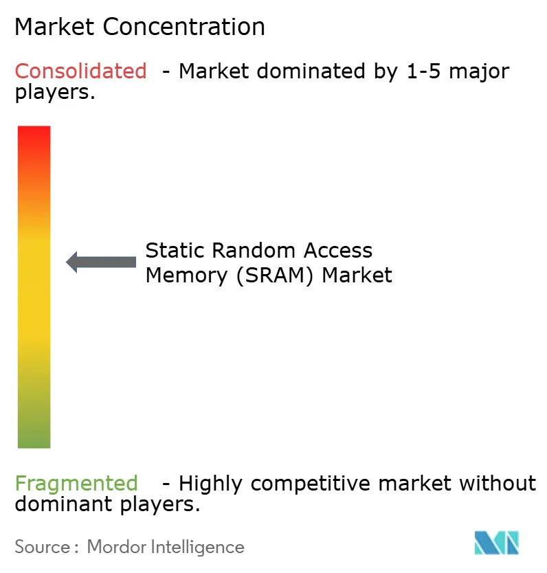
| Market Concentration | Medium |
Major Players *Disclaimer: Major Players sorted in no particular order Image © Mordor Intelligence. Reuse requires attribution under CC BY 4.0. | |
Static Random Access Memory (SRAM) Market Analysis by Mordor Intelligence
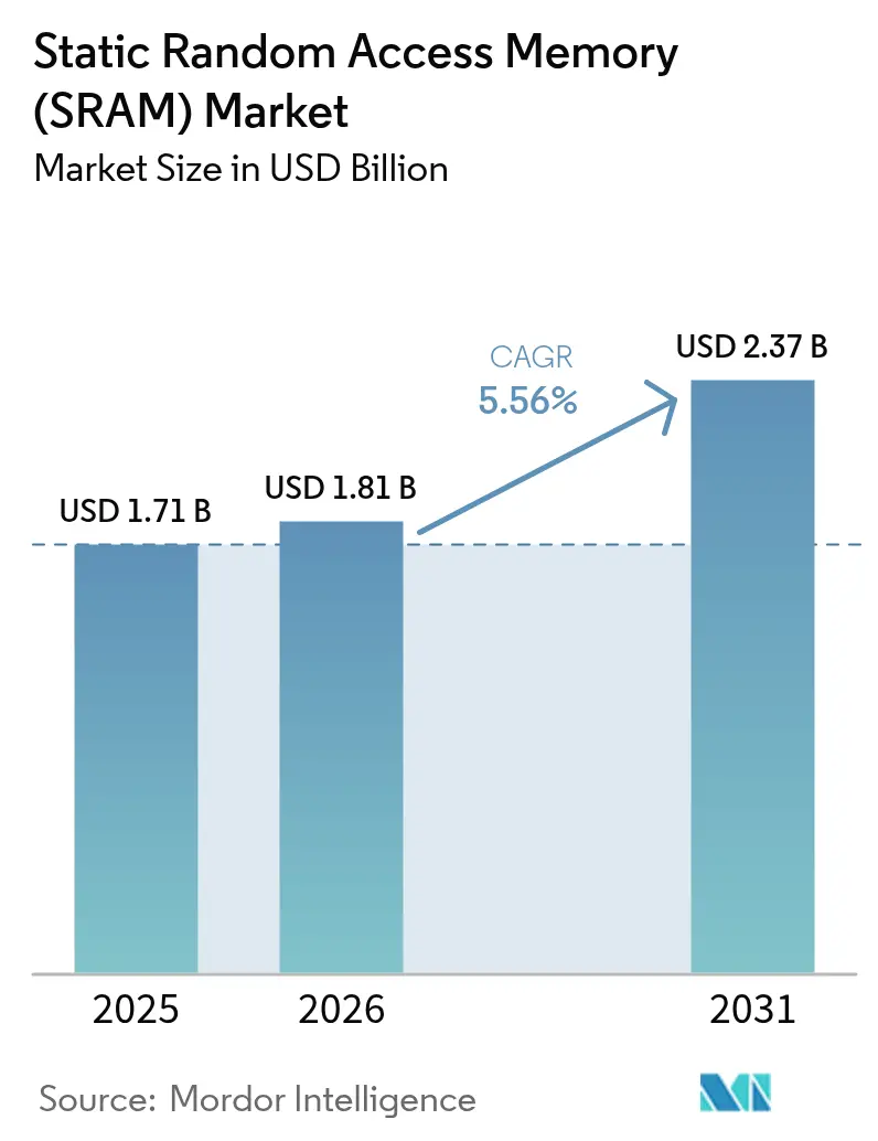
The Static Random Access Memory market size was valued at USD 1.71 billion in 2025 and estimated to grow from USD 1.81 billion in 2026 to reach USD 2.37 billion by 2031, at a CAGR of 5.56% during the forecast period (2026-2031). Growth reflected the transition toward AI-centric compute, 5G roll-outs, and real-time edge processing, all of which rely on SRAM’s ultra-low latency for cache hierarchies. Semiconductor vendors prioritized shrinking SRAM cells at 2 nm to support larger L2/L3 caches while keeping power budgets in check. Data-center modernization drove demand for high-speed buffers in switches and accelerators, whereas consumer device refresh cycles maintained a steady baseline. Supply-chain resilience became pivotal after the 2024 Taiwan earthquake disrupted foundry output, prompting geographic diversification initiatives. Meanwhile, emerging non-volatile memories such as MRAM intensified competitive pressure on conventional SRAM in battery-backed designs.[1]Everspin Technologies, “MRAM Replaces nvSRAM,” everspin.com
Key Report Takeaways
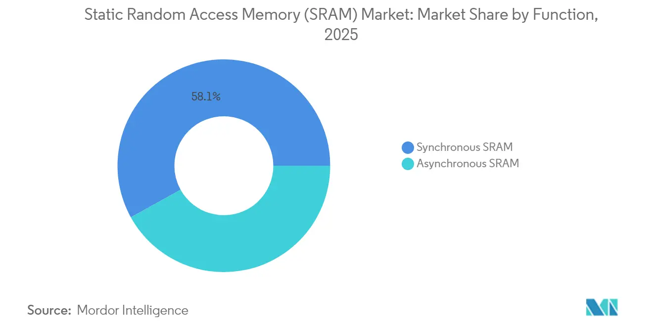
- By function, synchronous SRAM held 58.05% Static Random Access Memory market share in 2025; asynchronous SRAM posted the fastest 6.21% CAGR to 2031.
- By product type, pseudo-SRAM led with 54.02% revenue share in 2025, while non-volatile SRAM is projected to expand at an 8.42% CAGR.
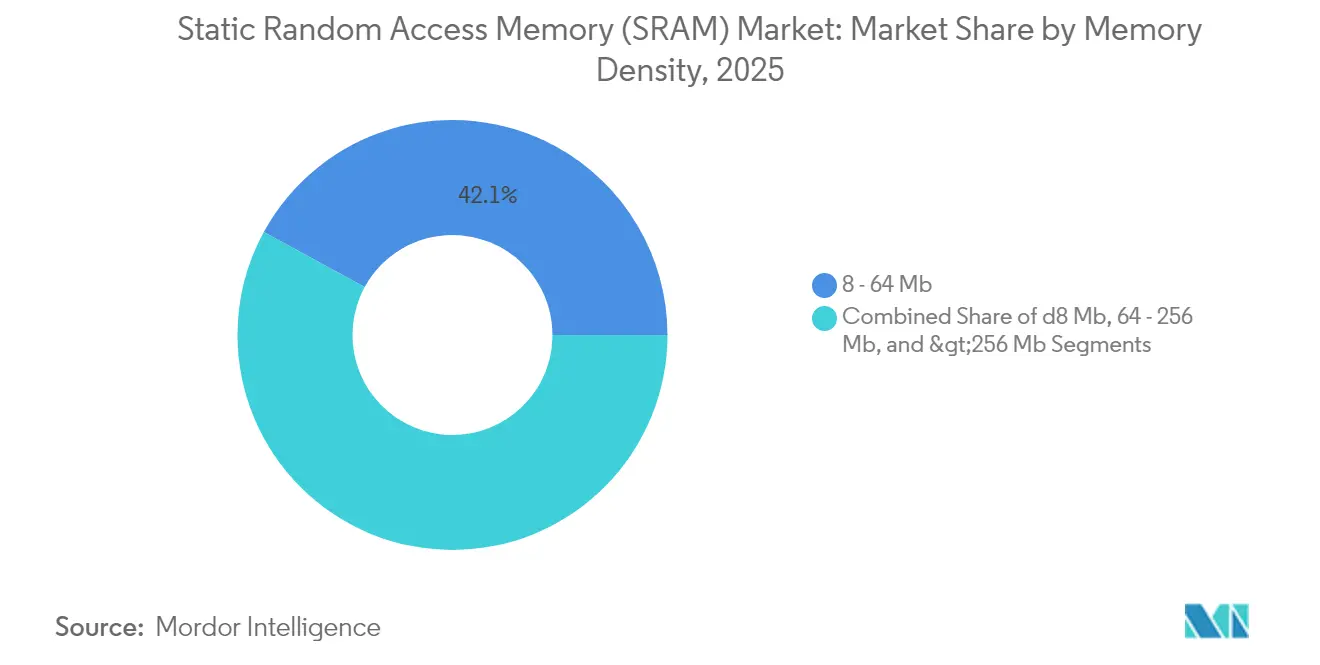
- By memory density, the 8–64 Mb tier accounted for 42.05% of the Static Random Access Memory market size in 2025; densities above 256 Mb are poised to grow at 7.26% CAGR.
- By end user, consumer electronics captured 45.92% revenue in 2025; automotive and aerospace are advancing at a 8.74% CAGR.
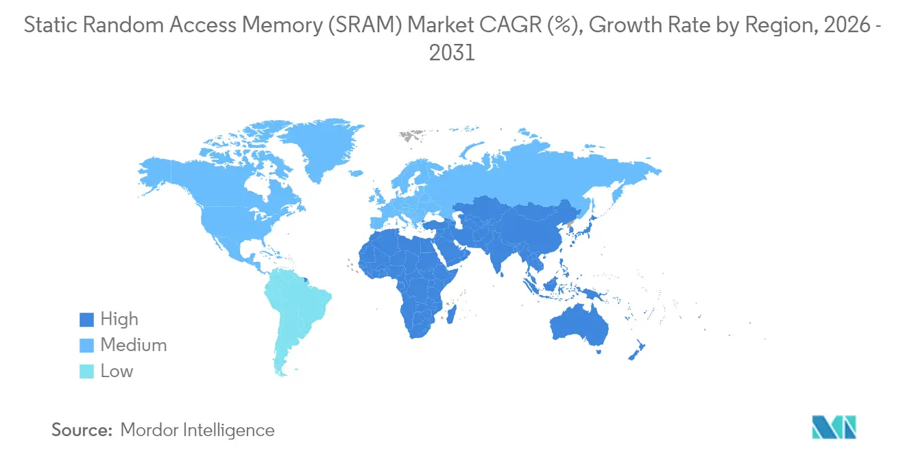
- By geography, Asia-Pacific commanded 61.02% share of the Static Random Access Memory market in 2025, whereas the Middle East and Africa are the fastest-growing regions at 7.23% CAGR.
Note: Market size and forecast figures in this report are generated using Mordor Intelligence’s proprietary estimation framework, updated with the latest available data and insights as of 2026.
Market Trends and Insights
Drivers Impact Analysis of Static Random Access Memory (SRAM) Market*
| Driver | (~) % Impact on CAGR Forecast | Geographic Relevance | Impact Timeline |
|---|---|---|---|
| Rising demand for faster cache memories | +1.2% | Global, concentrated in North America and Asia-Pacific | Medium term (2-4 years) |
| Data center and 5G network build-out | +1.0% | Global, with emphasis on Asia-Pacific and North America | Short term (≤ 2 years) |
| IoT and wearable device proliferation | +0.8% | Global, led by Asia-Pacific manufacturing hubs | Medium term (2-4 years) |
| 3D-integrated SRAM for chiplets | +0.6% | North America and Asia-Pacific advanced fabs | Long term (≥ 4 years) |
| Radiation-hardened SRAM for LEO satellites | +0.4% | Global, concentrated in North America and Europe | Long term (≥ 4 years) |
| In-memory AI accelerators adoption | +0.7% | Global, with North America and Asia-Pacific leadership | Medium term (2-4 years) |
| Source: Mordor Intelligence | |||
Rising demand for faster cache memories
Advanced CPUs and GPUs shipped in 2025 featured larger on-chip caches to cut inference latency, with Intel’s Xeon 6 showing a 1.4× performance lift tied to cache optimization. TSMC’s 2 nm platform delivered higher SRAM cell density than competing 18A nodes, giving hyperscale customers more L3 cache per watt. Marvell unveiled 2 nm custom SRAM that packs 6 Gb of low-power memory, reducing energy use by 66% versus prior nodes. Such innovations enabled AI accelerators to keep model parameters closer to compute units, sustaining throughput while containing DRAM traffic. Consequently, the Static Random Access Memory market benefited from recurring capacity upgrades across data-center and edge silicon.
Data-center and 5G network build-out
Cloud operators doubled rack densities to host AI servers, prompting wider use of SRAM-based packet buffers in top-of-rack switches. Microsoft tested 246–275 GHz wireless backplanes in server halls, where microsecond-scale buffering relied on high-speed SRAM. Cisco’s converged 5G transport promoted deterministic latency, necessitating deep SRAM queues in routers. Corning forecasts an 18× jump in fiber demand per AI rack, mirroring the scaling of switch buffers built on synchronous SRAM. This infrastructure wave reinforced near-term revenue visibility for the Static Random Access Memory market.
IoT and wearable device proliferation
Ultra-low-power edge chips powering health wearables adopted custom SRAM blocks that retained data at single-digit microwatts; Syntiant’s neural processors exemplified the trend. Edge2LoRa gateways embedded modest SRAM to preprocess sensor data, cutting backhaul bandwidth by 90%. Automotive MCUs such as Renesas R-Car integrate deterministic SRAM for over-the-air updates and ADAS workloads. Collectively, these deployments widened the customer base for asynchronous and pseudo-SRAM products tailored to energy constraints.
In-memory AI accelerators adoption
Research prototypes demonstrated photonic SRAM with embedded XOR logic executing at >10 GHz while consuming 13.2 fJ per bit, pointing to future compute-in-memory architectures. A 28 nm 36 Kb compute-in-memory SRAM reduced weight-update energy, paving the way for embedded AI inference engines. Everspin’s PERSYST positioned persistent memory for safety-critical AI workloads where data retention is required after power loss. These advances heightened interest in specialty SRAM that blends speed with programmability, further expanding the Static Random Access Memory market.
Restraints Impact Analysis of Static Random Access Memory (SRAM) Market*
| Restraint | (~) % Impact on CAGR Forecast | Geographic Relevance | Impact Timeline |
|---|---|---|---|
| High cost per bit vs. DRAM/NAND | -0.9% | Global, particularly impacting cost-sensitive applications | Short term (≤ 2 years) |
| Escalating power at ≤5 nm nodes | -0.7% | Advanced fabs in Asia-Pacific and North America | Medium term (2-4 years) |
| Emerging NVM (MRAM/ReRAM) displacement | -0.5% | Global, with early adoption in automotive and industrial | Long term (≥ 4 years) |
| Yield loss from lithography variability | -0.4% | Advanced process nodes globally | Medium term (2-4 years) |
| Source: Mordor Intelligence | |||
High cost per bit vs. DRAM/NAND
SRAM remained several times more expensive per bit than commodity DRAM, pressuring designers to trim usage in mass-market gadgets. DDR4 module prices climbed roughly 50% in H1 2025, illustrating volatility across the memory stack. Samsung leveraged tightening supply to lift LPDDR4 pricing, but that tactic risked accelerating OEM interest in hybrid SRAM-DRAM architectures to curb bills of materials. Consequently, the Static Random Access Memory market faced pushback in entry-level consumer segments until density-versus-cost trade-offs improved.
Emerging NVM (MRAM/ReRAM) displacement
Single-nanometer CoFeB/MgO magnetic tunnel junctions achieved sub-10 ns switching and ten-year retention, enabling MRAM to replace nvSRAM in rugged systems. Everspin marketed MRAM as a plug-in substitute for battery-backed SRAM, offering non-volatility without external capacitors. Automotive FPGA suppliers such as Lattice shifted from flash to MRAM configuration memory, showcasing real adoption.[2]Jim Tavacoli, “From Flash to MRAM,” Lattice Semiconductor, latticesemi.com If production costs fall further, a portion of the Static Random Access Memory market could migrate toward persistent alternatives.
*Our forecasts treat driver/restraint impacts as directional, not additive. The impact forecasts reflect baseline growth, mix effects, and variable interactions.
Static Random Access Memory (SRAM) Market Segment Analysis
By Function:
Performance hinges on synchronous architecturesSynchronous SRAM captured 58.05% Static Random Access Memory market share in 2025, underscoring its indispensability for deterministic cache operation in CPUs, GPUs, and network ASICs. Automotive MCUs used synchronous arrays to meet stringent real-time requirements for driver-assistance workloads. The segment will maintain leadership as advanced nodes extend frequency envelopes and reduce core voltages.
Asynchronous SRAM expanded at a 6.21% CAGR and increasingly served IoT wearables and edge gateways where power budgets override latency targets. Energy-efficient designs eliminated clock trees and simplified board layouts, a boon for battery-operated healthcare devices employing Syntiant’s neural coprocessors. This divergence emphasized the Static Random Access Memory market trend toward application-specific optimization rather than one-size-fits-all performance chasing.



By Product Type:
Cost-optimized pseudo-SRAM prevailsPseudo-SRAM held a 54.02% share in 2025 by embedding DRAM cells behind an SRAM-style interface, achieving higher density without refresh management at the system level. RAAAM Memory Technologies and NXP claimed 50% area and 10× power savings versus classic high-density SRAM, appealing to mass-market microcontrollers.
Non-volatile SRAM grew fastest at 8.42% CAGR as factories and vehicles demanded data integrity during brownouts. Industrial automation players selected nvSRAM modules to protect process variables, avoiding costly downtime. Although niche, this cohort enriched the Static Random Access Memory market landscape with value-added resilience features.
By Memory Density:
Mid-range remains sweet spotThe 8–64 Mb tier accounted for 42.05% of the Static Random Access Memory market size in 2025, matching typical L2/L3 cache footprints across mainstream CPUs. Alliance Memory’s 32 Mb fast SRAM in FBGA packaging illustrated continuous refinement in this zone.
>256 Mb devices posted a robust 7.26% CAGR as AI accelerators sought larger on-chip caches to minimize DRAM fetches. Micron projected automobiles would soon carry 90 GB of total memory, hinting at rising high-density SRAM demand in zonal controllers. Density evolution, therefore, mirrored compute-intensive workload growth underpinning the Static Random Access Memory market.
By End User:
Consumer volume vs. automotive velocityConsumer electronics generated 45.92% of 2025 revenue thanks to the vast scale of smartphones, tablets, and PCs. Micron and Samsung integrated LPDDR5X and on-board SRAM in the Galaxy S24, elevating mobile AI responsiveness.
Automotive and aerospace segments recorded a 8.74% CAGR as software-defined vehicles required a deterministic cache for sensor fusion and over-the-air reconfiguration. NXP’s S32K5 MCU with embedded magnetic RAM writes 15× faster than flash, demonstrating the appetite for high-reliability memory. Such momentum broadened the Static Random Access Memory market beyond traditional consumer refresh cycles.
Geography Analysis
APAC Static Random Access Memory (SRAM) Market
Asia-Pacific retained 61.02% Static Random Access Memory market share in 2025, fueled by Taiwan’s foundry dominance, South Korea’s memory innovation, and China’s scale-up efforts. SK Hynix’s rise to 36% of global DRAM output highlighted the region’s technology depth. Yet the 2024 Taiwan quake exposed concentration risk, prompting contingency fabs in Japan and Singapore. Japan projected semiconductor equipment sales of JPY 5.51 trillion (USD 38.35 billion) in FY26, underscoring continued capacity build-out.
MEA Static Random Access Memory (SRAM) Market
Middle East and Africa charted the fastest 7.23% CAGR, anchored by sovereign-fund spending to position the Gulf as a tri-continent data hub. Warehouse automation in the region was set for 17.5% annual growth to USD 1.6 billion by 2025, driving demand for reliable on-board caches. Africa’s energy projects earmarked USD 730 billion in new capex to 2030, requiring industrial control systems that lean on SRAM for deterministic response.
North America and Europe Static Random Access Memory (SRAM) Market
North America focused on AI datacenter roll-outs, while Europe doubled down on sovereignty through the EUR 43 billion Chips Act. STMicroelectronics secured EUR 5 billion (USD 5.4 billion) for a Silicon Carbide campus in Italy, widening regional competency in power electronics that also consume specialized SRAM. Talent shortages, however, threatened expansion, with ASML warning it might shift operations if immigration tightened. These contrasts highlight diverse regional levers shaping the Static Random Access Memory market.

Regulatory Landscape
SRAM trade and availability are being shaped by a tightening set of US trade, export-control, and public-procurement rules upstream of electronics design cycles. In January 2026, a US Section 232 action introduced a 25% ad valorem duty on specified imported semiconductors and derivatives effective January 15, 2026, adding landed-cost volatility for memory components used across networking, industrial, and automotive electronics.
On the technology-access side, in January 2026 the US Bureau of Industry and Security (BIS) revised its license review policy for advanced computing commodities, shifting certain exports to a case-by-case posture tied to US security testing. This affects how leading-edge SRAM embedded in advanced-node compute devices is routed and qualified. For defense and aerospace-grade SRAM, updated specifications also matter: DSCC 98537J:2026 refreshed requirements for radiation-hardened 128K x 8 CMOS/SOI static RAM, reinforcing qualification and sourcing constraints for rad-hard SRAM supply chains. Separately, US federal procurement is moving toward stricter source restrictions, with Section 5949 implementation plans calling for compliance requirements beginning December 23, 2026 for executive agencies obtaining semiconductor products traceable to certain Chinese companies.
Value Chain Analysis
The SRAM value chain runs from EDA and SRAM compiler or IP development to wafer fabrication (as embedded SRAM in SoCs and as discrete SRAM products), then assembly and test, followed by distribution to OEMs and EMS providers serving consumer electronics, communications infrastructure, industrial systems, and automotive or aerospace. Supply is split between IDMs that ship discrete SRAM and memory-rich MCUs, and fabless designers that rely on foundries where embedded SRAM competes for wafer starts alongside leading-edge logic, image sensors, and other high-margin products. As a result, allocation and cycle timing are key determinants of SRAM availability.
Upstream inputs include high-purity silicon wafers, specialty gases, and advanced photoresists, and broader semiconductor material bottlenecks continue to influence lead times. Asia-Pacific remains central to both production and consumption, and the 2024 Taiwan earthquake underscored how concentrated fabrication footprints can translate into output disruptions. That has driven efforts toward dual-sourcing and geographic diversification, and in 2026 supply-chain readiness and visibility have become a focal point for the ecosystem, with planning, logistics resilience, and multi-tier supplier management shaping how quickly SRAM-bearing devices can be qualified and delivered.
Competitive Landscape
The market displayed moderate consolidation around integrated device manufacturers and foundry-aligned challengers. Samsung, SK Hynix, and Micron fortified positions by scaling HBM roadmaps; Samsung accelerated its Pyeongtaek wafer fab to seize HBM4 business. SK Hynix partnered with TSMC on advanced packaging to sustain bandwidth leadership.[4]SK hynix, “Partners with TSMC to Strengthen HBM Leadership,” skhynix.com
At the IP and specialty layer, GSI Technology and Cypress targeted low-latency networking gear, while newcomers such as Numem planned MRAM chiplets promising HBM-class throughput by 2025. Imec, TSMC, and Samsung-IBM each demonstrated CFET SRAM prototypes with 40% cell-area reduction, anticipating 3D stacked logic-memory hybrids.
Emergent niches included radiation-hardened 18T cells for LEO satellites that improved read stability while lowering standby power. Funding from the European Innovation Council enabled RAAAM to advance on-chip pseudo-SRAM for MCU markets, illustrating how regional policy catalyzed new entrants. Competitive advantage thus pivoted on packaging innovation, specialty process know-how, and intellectual-property breadth, all shaping future Static Random Access Memory market positioning.
Static Random Access Memory (SRAM) Industry Leaders
Renesas Electronics Corporation
STMicroelectronics N.V.
Toshiba Corporation
Cypress Semiconductor
Integrated Silicon Solution, Inc. (ISSI)
- *Disclaimer: Major Players sorted in no particular order
Static Random Access Memory (SRAM) Market Companies Covered in this Report
- GSI Technology Inc.
- Cypress Semiconductor Corp. (Infineon)
- Renesas Electronics Corp.
- Integrated Silicon Solution Inc.
- Alliance Memory Inc.
- Everspin Technologies Inc.
- Samsung Electronics Co., Ltd.
- Toshiba Electronic Devices & Storage Corp.
- STMicroelectronics N.V.
- SK hynix Inc.
- Micron Technology Inc.
- Nanya Technology Corp.
- Winbond Electronics Corp.
- Elite Semiconductor Memory Technology Inc.
- Chiplus Semiconductor Corp.
- Powerchip Semiconductor Mfg. Corp.
- Puya Semiconductor Technology Co., Ltd.
- Lyontek Inc.
- ON Semiconductor Corporation
- Texas Instruments Incorporated
- Integrated Device Technology Inc.
- NXP Semiconductors N.V.
- Etron Technology Inc.
- Espressif Systems (Shanghai) Co., Ltd.
- SKYHigh Memory Ltd.
Read Analysis of Static Random Access Memory (SRAM) Companies

Market Opportunities and Future Outlook
Near-term whitespace is concentrated in SRAM-heavy architectures that reduce data movement for AI inference and deterministic edge processing, along with specialty-grade SRAM for high-reliability environments. The market is also creating opportunities around higher-density cache hierarchies and fast buffers in network and accelerator silicon, as vendors pursue larger L2 or L3 footprints and lower latency within tight power budgets. This is tied to ongoing work to shrink SRAM cells at 2 nm, alongside architectural approaches such as 3D integration and chiplet-based partitioning.
Automotive and industrial electronics are adding design-in pathways for robust, ECC-protected on-chip SRAM and memory-assist features where functional safety and real-time response drive system requirements. Evidence of this shift appears in new MCU and SoC-class platforms that integrate multi-megabyte SRAM blocks, as well as in advanced memory structures demonstrated for automotive SoCs, including dedicated SRAM intended to enhance ECC parity behavior in emerging TCAM architectures. Competitive positioning increasingly favors suppliers that co-optimize SRAM design technology with advanced packaging and integration, rather than relying only on dimensional scaling. At the same time, alternative non-volatile memories such as MRAM continue to pressure battery-backed SRAM use cases, pushing SRAM toward more performance-critical roles.
Recent Industry Developments in Static Random Access Memory (SRAM) Market
- February 2026: Renesas disclosed a configurable ternary content-addressable memory (TCAM) design on a 3 nm FinFET process at ISSCC 2026 that incorporates dedicated SRAM to improve ECC parity behavior for automotive functional safety. The announcement highlights how SRAM is being architected alongside specialized memories to meet deterministic, safety-driven workloads in automotive SoCs.
- July 2025: Renesas introduced RA8P1 microcontrollers with AI acceleration, integrating 2 MB of ECC-protected SRAM alongside on-chip MRAM. This reinforces the trend toward larger, protected SRAM blocks inside MCUs to keep latency-sensitive inference and control tasks close to compute while reducing dependence on external memory.
- April 2025: Alliance Memory launched a 32 Mb fast CMOS SRAM (AS7CW2M16-10BIN) in a 48-ball FBGA (6 mm x 8 mm) package for industrial, networking, and automotive designs. The product targets space-constrained boards and refreshes the discrete SRAM lineup used for buffers, scratchpad memory, and deterministic local storage.


Static Random Access Memory (SRAM) Market Report Scope and Research Methodology
Market Definition and Coverage
This market covers revenues generated from static random access memory (SRAM) devices sold into end use applications where fast, low latency memory is required, and values are counted at the point where SRAM is supplied to electronics manufacturing.
Scope exclusions: We exclude broader memory categories such as DRAM and NAND flash, and we do not count downstream device markups from finished electronics.
Segments Covered in This Report
- By Function
- Asynchronous SRAM
- Synchronous SRAM
- By Product Type
- Pseudo SRAM (PSRAM)
- Non-Volatile SRAM (nvSRAM)
- Other Product Types
- By Memory Density
- ≤8 Mb
- 8 – 64 Mb
- 64 – 256 Mb
- >256 Mb
- By End User
- Consumer Electronics
- Industrial
- Communication Infrastructure
- Automotive and Aerospace
- Other End Users
- By Geography
- North America
- United States
- Canada
- Mexico
- South America
- Brazil
- Argentina
- Rest of South America
- Europe
- Germany
- United Kingdom
- France
- Italy
- Russia
- Rest of Europe
- Asia-Pacific
- China
- Japan
- South Korea
- India
- Taiwan
- Rest of Asia-Pacific
- Middle East and Africa
- Middle East
- Turkey
- Israel
- GCC Countries
- Rest of Middle East
- Africa
- South Africa
- Nigeria
- Rest of Africa
- Middle East
- North America
Data Sources, Market Sizing, and Validation
Desk Research
Desk work starts by building a clean fact base on SRAM demand and supply, then we map how SRAM fits into the broader semiconductor landscape. We rely on public sources such as USITC and UN Comtrade trade statistics, World Semiconductor Trade Statistics summaries, OECD and World Bank macro series, and central bank FX releases to keep currency conversions consistent.
On the technical and application side, we review sources such as IEEE publications and patent databases to understand how SRAM use changes by node, density, and embedded versus standalone choices. We also use company annual reports, earnings call transcripts, investor presentations, and reputable press to identify capacity moves, product refresh cycles, and any pricing commentary. When needed, paid subscriptions for company financials and intelligence, news and financials, and patent databases help with faster cross-checking and timeline validation. These sources are illustrative, and many other public references were also used for data collection, validation, and clarification.
Primary Interviews and Surveys
Primary work is used to pressure test the desk assumptions and to fill gaps that are not visible in public data, especially around SRAM content per device and realistic ASP movement by density. We speak with a mix of chip and IP ecosystem participants, distribution and channel experts, and demand side users across APAC, EMEA, and the Americas, so the model is not pulled toward a single region or one end market.
Distribution of primary research fieldwork respondents
| Company type | Respondent position | Region |
|---|---|---|
| Top tier: 36% | CXOs: 14% | APAC: 50% |
| Mid tier: 50% | Functional/Unit leaders: 40% | EMEA: 31% |
| Smaller Players: 14% | Managers: 46% | Americas: 19% |
Market-Sizing & Forecasting
Sizing starts with a top-down build where semiconductor demand signals are reconstructed by region, then filtered into an SRAM demand pool using application level memory content and adoption rates. The model is anchored on practical inputs, including wafer capacity and utilization signals tied to logic and memory supply, the mix of synchronous versus asynchronous usage in key designs, typical density shifts, and pricing behavior by density band that shows up through channel feedback.
Once the demand pool is formed, it is corroborated through selective bottom-up approximations, including sampled supplier revenue disclosures, channel checks on volume direction, and ASP times shipment-style math for representative SRAM categories. When a data point is missing for a country or an end use, we backfill using proxy indicators such as electronics production growth, import trends, and validated share splits collected in interviews, before totals are recalibrated.
For forecasting, we use scenario analysis supported by a light multivariate regression layer, where variables such as electronics output, semiconductor cycle indicators, AI and data center buildout momentum, and automotive electronic content trends shape the path. Final year values are kept consistent with what experts consider feasible for supply response and pricing normalization, so the forecast does not overreact to a single year spike.
Data Validation & Update Cycle
Validation is done through repeated cross checks, where model outputs are compared with independent signals like regional semiconductor shipment direction, trade flows for relevant device categories, and reported commentary on pricing and lead times. If a variance looks abnormal, the assumption is reopened, and we re-contact selected experts to confirm whether the change is structural or only a short cycle effect.
Before sign off, the analysis goes through multi-step internal reviews, including logic checks on inputs, unit consistency checks, and year-over-year movement checks so growth remains explainable. The report is refreshed annually, and interim updates are made when a material event occurs, such as a major capacity move or a demand shock. Right before delivery, a final pass is completed so clients receive the most current view available.
Mordor Intelligence's Static Random Access Memory Market Size Measured Against Other Published Estimates
It is common to see different SRAM market values across publications, even when the same technology name is used. The gaps usually come from what each study counts as SRAM revenue, which year is treated as the current reference point, and how pricing and density shifts are carried into the forecast.
Some estimates appear to lean toward a narrower static RAM view, and they often keep product scope tight and do not fully account for newer SRAM variants used in higher value applications. In the Mordor Intelligence estimate, the SRAM total is counted across asynchronous and synchronous SRAM plus PSRAM and nvSRAM categories, and it is then validated against region level demand signals and interview-based share splits to avoid over or under counting.
Benchmark comparison
| Source | Market Size | Gaps in Research Methodology |
|---|---|---|
| Mordor Intelligence | USD 1.81 B (2026) | |
| Global Consultancy A | USD 0.47 B (2024) | Uses an earlier base year and a more conservative scope that tends to treat the market as conventional static RAM, which can leave out some SRAM adjacent product types and dampen implied ASP progression. |
| Industry Research Desk B | USD 0.72 B (2025) | Reports a smaller 2025 value that likely reflects tighter inclusion rules and a different currency timing, and the long forecast horizon can also smooth near term up cycles in pricing and volume. |
The spread across figures is mainly explained by year alignment and what gets included under the SRAM label, followed by how price per bit is expected to move as density shifts. By keeping inputs tied to observable demand indicators, and by using interview checks to confirm mix and adoption, our estimate stays traceable and repeatable even when public data is incomplete.


Key Questions Answered in the Report
What is the current value of the Static Random Access Memory market?
The market reached USD 1.81 billion in 2026 and is forecast to climb to USD 2.37 billion by 2031.
Which region dominates the Static Random Access Memory market revenue?
Asia-Pacific accounted for 61.02% of global revenue in 2025, anchored by Taiwan’s and South Korea’s manufacturing ecosystems.
Which Static Random Access Memory market segment is growing fastest?
Automotive and aerospace applications are expanding at a 8.74% CAGR as vehicles adopt software-defined architectures requiring low-latency caches.
How is emerging MRAM technology impacting SRAM demand?
MRAM offers non-volatility and lower standby power, challenging SRAM in battery-backed and rugged systems, potentially diverting share over the long term.
What density class is most common in today’s SRAM chips?
The 8–64 Mb range captured 42.05% of 2025 sales because it aligns with mainstream processor cache sizes.
Why did synchronous SRAM outrun asynchronous types in revenue share?
Clock-synchronized designs provide deterministic timing essential for high-performance CPUs, GPUs, and networking ASICs, securing 58.05% market share in 2025.
Page last updated on: