Silicon Photonics Market Size and Share
Market Overview
| Study Period | 2019 - 2030 |
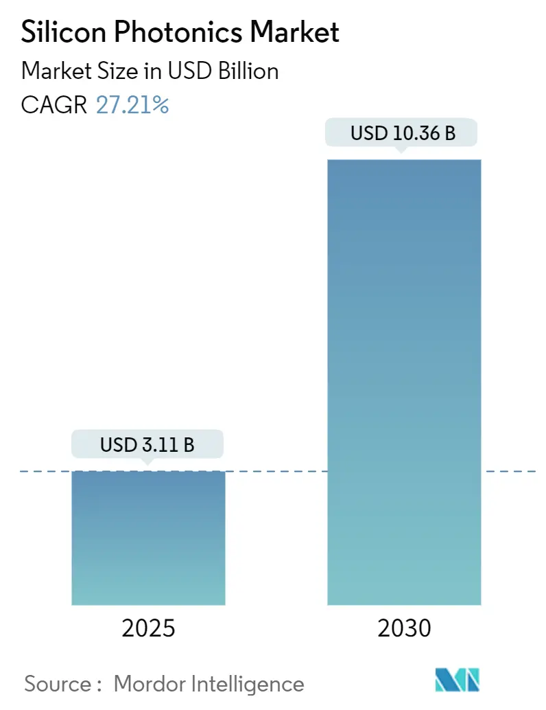
| Market Size (2025) | USD 3.11 Billion |
| Market Size (2030) | USD 10.36 Billion |
| Growth Rate (2025 - 2030) | 27.21% CAGR |
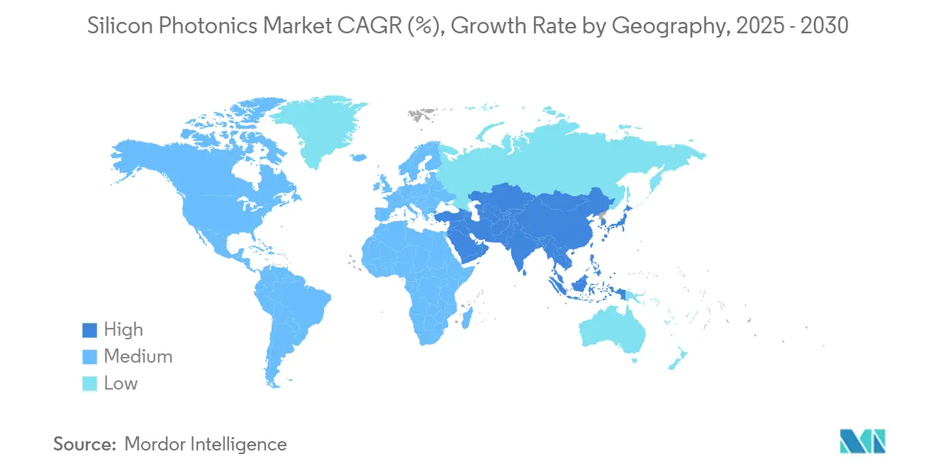
| Fastest Growing Market | Asia Pacific |
| Largest Market | North America |
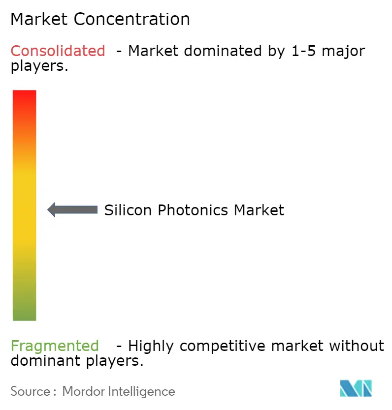
| Market Concentration | Medium |
Major Players*Disclaimer: Major Players sorted in no particular order Image © Mordor Intelligence. Reuse requires attribution under CC BY 4.0. |
|
Silicon Photonics Market Analysis by Mordor Intelligence
The silicon photonics market generates USD 3.11 billion in 2025 and is forecast to advance at a 27.21% CAGR, reaching USD 10.36 billion by 2030. Demand is accelerating as hyperscale data centers shift from 800 G to 1.6 T optical links, automotive OEMs integrate frequency-modulated continuous-wave LiDAR, and government incentives expand domestic semiconductor capacity. North America retains leadership, yet Asia Pacific is closing the gap through large-scale fab expansions aligned with 5G, AI and sovereign-supply objectives. Competing material platforms such as indium phosphide spur innovation but also intensify price pressure, while thermal-budget ceilings above 70 °C force new cooling architectures. M&A activity underscores the rising strategic value of photonic integration, with network equipment vendors, foundries and cloud providers securing design teams and wafer capacity ahead of looming supply constraints.
Key Report Takeaways
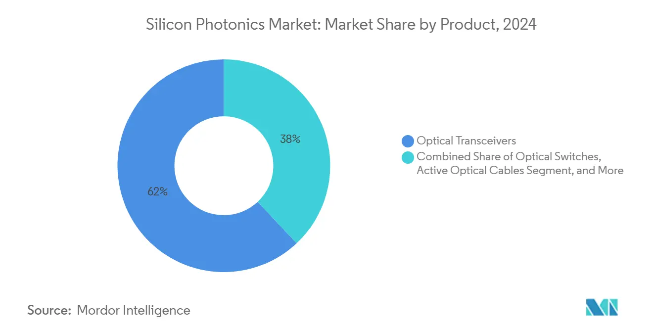
- By product, optical transceivers led with 62% revenue share in 2024; wafer-level test systems are forecast to expand at a 28.1% CAGR to 2030.
- By component, active components held 58% revenue share in 2024, while passive components are set to register a 29.7% CAGR through 2030.
- By wafer size, the 300 mm segment captured 68% share of the silicon photonics market size in 2024 and is advancing at a 28.4% CAGR through 2030.
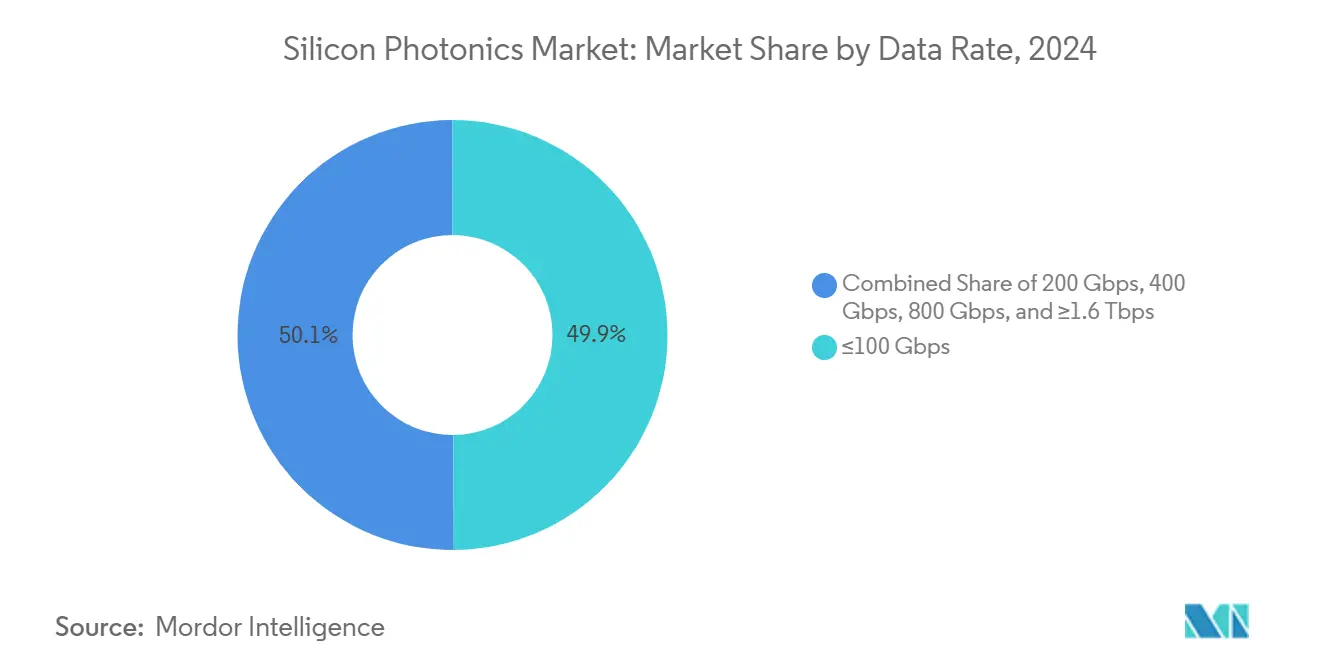
- By data rate, ≤100 Gbps accounted for 50% of the silicon photonics market size in 2024; the 800 Gbps segment shows the highest projected CAGR at 31.2% to 2030.
- By application, data centers & HPC held 72% share of the silicon photonics market size in 2024; automotive & autonomous vehicles is projected to grow at a 32.4% CAGR through 2030.
- By end-user, hyperscale cloud providers commanded 68% share in 2024, while automotive OEMs & Tier-1 suppliers are expected to post a 34.7% CAGR up to 2030.
- By geography, North America led with 38% of the silicon photonics market share in 2024, while Asia Pacific is forecast to expand at a 35.1% CAGR through 2030.
Global Silicon Photonics Market Trends and Insights
Drivers Impact Analysis
| Driver | (~) % Impact on CAGR Forecast | Geographic Relevance | Impact Timeline |
|---|---|---|---|
| Energy-efficient co-packaged optics in hyperscale data centers | +15% | North America, spillover to APAC | Medium term (2-4 years) |
| Carbon-reduction mandates for low-power interconnects | +12% | EU, gradual uptake in North America | Medium term (2-4 years) |
| 5G fronthaul/backhaul upgrade to 400/800 G | +14% | China, South Korea, Japan | Short term (≤2 years) |
| Automotive Level-3 LiDAR programs using FMCW | +11% | China & EU | Medium term (2-4 years) |
| Defense funding for quantum-secure photonics | +9% | United States, secondary EU & Israel | Long term (≥4 years) |
| Government incentive schemes expanding photonic fabs | +13% | US, EU, Asia | Medium term (2-4 years) |
Source: Mordor Intelligence
Energy-efficient Co-Packaged Optics Adoption in Hyperscale Data Centers
Directly embedding optical engines beside switch ASICs trims electrical-optical conversions and cuts rack-level power draw by up to 40%. Google’s optical circuit switching trials validate latency gains, and both NVIDIA and Marvell now sample proprietary co-packaged modules that streamline board layouts for AI clusters. The silicon photonics market benefits as switch makers standardize optical die-to-die interfaces, creating a volume pull for integrated lasers, modulators and photodetectors packaged on 300 mm wafers.[1]TSMC, “2025 North America Technology Symposium,” tsmc.com
Carbon-Reduction Mandates Driving Low-Power Optical Interconnects
EU data-center sustainability rules target significant energy savings, prompting operators to phase out copper backplanes. Photonic links show 30% lower consumption in 100 Gbps channels while maintaining reach. Cloud providers publish carbon-neutral roadmaps, accelerating multi-vendor qualification of 400 G and 800 G silicon photonics modules that align with corporate ESG metrics and local green-deal incentives.
5G Fronthaul/Backhaul Upgrade Fueling 400/800 G Modules
Rapid 5G rollout triggers fiber densification, and telecom operators standardize on pluggable 400 G QSFP-DD and emerging 800 G OSFP optics for mid-haul rings. Integrated photonics minimises footprint and power cost per bit, allowing radio-access vendors to compress equipment shelters. Asian public-private broadband programs add procurement scale, reinforcing the silicon photonics market as the preferred on-board optics platform for multi-wavelength coherent modules.
Automotive Level-3 LiDAR Programs Leveraging FMCW Silicon Photonics
OEMs escalate FMCW LiDAR design-ins to surpass 300 m detection range with millimetre-level resolution. Silicon integration shrinks sensor bill-of-materials and simplifies alignment, advancing cost targets for 2026 model years.[2]Optics.org, “CES 2024: New Lidars for Old,” optics.orgPartnerships between photonics designers and tier-1 suppliers create modular transmit-receive chips that withstand automotive thermal cycles, broadening the silicon photonics industry footprint beyond datacom.
Restraints Impact Analysis
| Restraint | (~) % Impact on CAGR Forecast | Geographic Relevance | Impact Timeline |
|---|---|---|---|
| Restraint | (~) % Impact on CAGR Forecast | Geographic Relevance | Impact Timeline |
| Thermal budget limits in silicon above 70 °C | -8% | Global, high-density compute sites | Medium term (2-4 years) |
| Lack of standardized packaging inflating NRE | -7% | Global, acute for small vendors | Short term (≤2 years) |
| Competition from InP & polymer photonics >1.55 µm | -6% | North America & Europe | Medium term (2-4 years) |
| Limited 300 mm foundry capacity extending lead times | -9% | Global, volume applications | Short term (≤2 years) |
Source: Mordor Intelligence
Thermal Budget Limitations in Silicon Substrates Above 70 °C
Optical phase stability drops at elevated junction temperatures, forcing elaborate heat sinks and liquid cooling in tightly packed AI servers.[3]U.S. Department of Energy, “Energy Efficiency Scaling for Two Decades Research,” energy.govResearch programs explore heterogeneous materials with higher thermal conductivity and temperature-insensitive resonator designs, yet these add process steps and cost, tempering near-term adoption in edge compute nodes.
Lack of Standardized Packaging Elevating NRE Costs
Absence of unifying assembly guidelines drives bespoke fiber attach, hermetic sealing and RF launch structures. Large vendors amortize tooling across high volumes, whereas startups face steep upfront expenses that delay product release. International packaging alliances are drafting reference blueprints, but broad acceptance will take several design cycles.
Segment Analysis
By Product: Optical Transceivers Sustain Leadership, Test Systems Gain Momentum
Optical transceivers generated 62% revenue in 2024 as hyperscalers deployed 800 G optics and qualified early 1.6 T line-cards.[4]Intel, “Intel Silicon Photonics,” intel.comDesign wins increasingly bundle integrated drivers and thermal monitors, easing system design and lowering capex per port. The silicon photonics market continues to pivot toward full-stack transceiver solutions that collapse laser, modulator and photodetector in one monolithic die. Market entrants differentiate through modal multiplexing and CW-laser integration that improve power efficiency.
Wafer-level test systems show the fastest expansion at 28.1% CAGR, propelled by tighter yield requirements at 400-G symbols /s and above. Parallel optical probing shrinks cycle time and raises throughput to match 300 mm line capacity. Vendors invest in AI-assisted defect analytics, linking parametric drift to fab data and enabling predictive maintenance. Broader use of automated optical test shortens time-to-qualification for new tape-outs, buttressing scale-up of the silicon photonics market.
Note: Segment shares of all individual segments available upon report purchase
By Component: Active Devices Dominate as Passive Innovation Accelerates
Active components maintained a 58% share in 2024, reflecting persistent demand for compact CW lasers, high-extinction modulators and low-dark-current photodiodes. Integrated multiplexers now ship in 112Gbaud PAM4 transceivers, demonstrating stable drive voltages at 55 °C case temperatures. Chip makers refine heterogeneous III-V laser attach, boosting wall-plug efficiency and reducing optical loss across epitaxial interfaces.
Passive components post the highest 29.7% CAGR as fabs iterate low-loss waveguides, lattice filters and arrayed-waveguide gratings tailored for 400G ZR+. Ultralow-roughness etch profiles cut insertion loss below 0.5 dB/cm, essential for co-packaged optics. Printed photonic circuit boards embedding glass waveguides promise board-level optical backplanes, further expanding addressable opportunities for the silicon photonics market.
By Wafer Size: 300 mm Captures Scale Advantage
The 300 mm tranche represented 68% revenue in 2024 and leads growth at 28.4% CAGR. Larger substrates elevate die output per run and enable advanced lithography alignment critical for multi-layer photonic-electronic stacks. Foundries leverage existing logic lines to add deep-UV waveguide modules, unlocking cost parity with pluggable copper interconnects for 100 m reaches. New pilot lines under construction in the US, EU and Japan will widen regional supply and lift overall silicon photonics market capacity.
The 200 mm segment remains relevant for legacy telecom chipsets and R&D prototypes, where tool amortisation is complete and exotic materials can be inserted with minimal disruption. Sub-150 mm fabs focus on niche sensors, quantum photonics and academic research, acting as incubation grounds for future IP that migrates to 300 mm once volumes justify transitio
By Data Rate: ≤100 Gbps Holds Volume; 800 Gbps Accelerates Adoption
≤100 Gbps modules accounted for half of shipments in 2024, supporting enterprise switching, 5G fronthaul and consumer optics. Continuous cost erosion keeps average selling prices attractive, sustaining run-rate volumes even as top-end speeds rise. The silicon photonics market benefits from pin-for-pin upgrades that swap copper DACs with optical AOCs in space-limited racks.
The 800 Gbps class surges at 31.2% CAGR as AI clusters standardize on 51.2 T and 102.4 T switches that require 100 G lane technology. Multi-core fibre and 4:1 gearbox optics compress link budgets, while DSPs integrate forward-error-correction to counter fibre non-linearities. Early demonstrations of 1.6 T co-packaged engines confirm a clear path to double-rate migration within the forecast horizon.
Note: Segment shares of all individual segments available upon report purchase
By Application: Data Centers & HPC Anchor Demand, Automotive Scales Rapidly
Data centers & high-performance computing commanded 72% share in 2024, reflecting the decisive role of optical interposers in removing copper bottlenecks from AI accelerators. Integrated photonics allows switch-to-server disaggregation, enabling rack-scale supercomputing with lower energy per bit. Co-design between optical, thermal and power delivery teams becomes table stakes for next-generation colocation hubs.
Automotive & autonomous vehicles post a 32.4% CAGR as lidar, in-vehicle backbone and zonal architectures shift to photonic links. Tier-1 suppliers qualify photonic radar hybrids that fuse mmWave and FMCW lidar for redundancy. Regulatory momentum for safety standards reinforces volume outlook, securing a stable second-pillar segment for the silicon photonics industry.
By End-User: Hyperscale Cloud Providers Maintain Lead, Automotive OEMs Surge
Hyperscale operators held 68% share in 2024 due to relentless AI and cloud capex. Internal silicon photonics design teams co-optimize optics with custom AI silicon, squeezing latency budgets. Multi-sourcing strategies lock in parallel foundry capacity, mitigating geopolitical supply risk and underpinning the long-term growth of the silicon photonics market.
Automotive OEMs & tier-1 suppliers expand at 34.7% CAGR, leveraging photonics to meet sensor fusion and infotainment bandwidth needs. Direct procurement of photonic dies signals a strategic pivot to secure control over critical safety components. Telecom operators, medical device firms and defense agencies round out demand, each aligning photonic integration to specific regulatory or performance imperatives.
Geography Analysis
North America generated 38% of 2024 revenue, buoyed by CHIPS Act grants and rapid deployment of AI mega-campuses. Albany NanoTech’s elevation to national research hub and private-sector investments from cloud leaders lock in a domestic ecosystem spanning design, packaging and advanced testing. Ongoing evolution of the silicon photonics market in the region hinges on seamless collaboration between foundries and equipment vendors to overcome wafer-level thermal setbacks.
Asia Pacific records the fastest 35.1% CAGR through 2030 as China, Japan and South Korea race to anchor sovereign supply chains. Government subsidies cover fab tools, training and metrology, while 5G densification and local AI start-ups guarantee offtake. Japanese investments in 300 mm GaAs-on-silicon lasers position domestic suppliers for export-oriented growth, reinforcing the global breadth of the silicon photonics market.
Europe sustains momentum through the EU Chips Act’s multi-billion-euro financing and a strong industrial base in automotive, industrial automation and research photonics. Carbon-neutral data-center mandates further encourage photonic adoption. South America and the Middle East & Africa open new footholds for telecom and edge-cloud deployments, but still rely on imported dies and packaging services, a gap that multinational OEMs strive to close via localized assembly partnerships.
Competitive Landscape
Competition is moderate, with integrated-device manufacturers, network equipment vendors and fab-lite start-ups vying for design wins. Intel has shipped more than 8 million photonic integrated circuits and recently unveiled a 4 Tbps compute interconnect chiplet that anchors its co-packaged optics roadmap. Cisco and Broadcom embed silicon photonics in 51.2 T switches, bundling software-defined networking to lock customers into vertically optimized platforms.
Specialist innovators such as Ayar Labs push chip-to-chip optical I/O that replaces parallel copper buses, while POET Technologies markets an interposer architecture that halves laser attach cost. Strategic acquisitions continue: Nokia moved to acquire Infinera in 2024 to supplement coherent DSP know-how with internally sourced lasers, showcasing the premium placed on end-to-end optical control.
Foundries including TSMC, GlobalFoundries and Tower focus on adding III-V laser bonding, deep-trench isolation and on-wafer testing to de-risk volume production for fabless customers. Equipment suppliers respond with photonic-specific align & attach tools, further industrializing processes that underpin the silicon photonics market. Over the forecast period, vendor differentiation will hinge on power-per-bit metrics, tight integration with AI accelerators and guaranteed wafer slots during capacity crunches.
Silicon Photonics Industry Leaders
-
Sicoya GMBH
-
Intel Corporation
-
Cisco Systems Inc.
-
Lumentum Operations LLC (Lumentum Holdings Inc.)
-
Juniper Networks Inc.
- *Disclaimer: Major Players sorted in no particular order
Recent Industry Developments
- May 2025: Coherent reported FY25 revenue of USD 5.8 billion, up from USD 4.7 billion in FY24, and highlighted expanded InP laser capacity to meet AI optical module demand.
- May 2025: Soitec noted strong uptake of Photonics-SOI wafers and joined the SEMI Silicon Photonics Industry Alliance to accelerate ecosystem collaboration.
- May 2025: NVIDIA posted Q1 FY26 revenue of USD 44.1 billion and introduced silicon photonics-based networking switches for next-generation AI platforms.
- May 2025: Aeluma secured a U.S. Department of Energy contract for low-cost SWIR photodetectors and reported 265% year-on-year revenue growth.
- April 2025: TSMC highlighted co-packaged optics progress at its North America Technology Symposium, reinforcing photonics as a “More-than-Moore” pillar.
- March 2025: Dexerials showcased a waveguide-type high-speed photodetector targeting transceivers above 1.6 Tbps.
Global Silicon Photonics Market Report Scope
Silicon photonics is a technology for fabricating optical and electronic integrated circuits on silicon microchips. Manufacturing photonic circuits using CMOS technologies, also known as silicon photonics, not only offers the scale of semiconductor wafer-scale fabrication but also enables advantages in new electronics applications using the properties of light in computation, communication, sensing, and imaging. Moreover, silicon photonics is a growing technology that uses optical rays to transfer data within computer chips.
The silicon photonics market is segmented by application (data centers and high-performance computing, telecommunications, automotive, and other applications) and geography (North America, Europe, Asia-Pacific, and the Rest of the World). The market sizes and forecasts are provided in terms of value in USD for all the above segments.
| By Product | Optical Transceivers | |||
| Optical Switches | ||||
| Active Optical Cables (AOCs) | ||||
| Silicon Photonic Sensors | ||||
| Wafer-level Test Systems | ||||
| Multiplexers/De-Multiplexers | ||||
| Attenuators and Modulators | ||||
| Others | ||||
| By Component | Active Components | Lasers | ||
| Modulators | ||||
| Photodetectors | ||||
| Passive Components | Waveguides | |||
| Filters | ||||
| Couplers | ||||
| Others | ||||
| By Wafer Size | 300 mm | |||
| 200 mm | ||||
| 150 mm and Below | ||||
| By Data Rate | ?100 Gbps | |||
| 200 Gbps | ||||
| 400 Gbps | ||||
| 800 Gbps | ||||
| ?1.6 Tbps | ||||
| By Application | Data Centers and High-Performance Computing | |||
| Telecommunications | ||||
| Automotive and Autonomous Vehicles | ||||
| AR/VR and Consumer Electronics | ||||
| Healthcare and Life Sciences | ||||
| Defense and Aerospace | ||||
| Quantum Computing | ||||
| Others | ||||
| By End-User | Hyperscale Cloud Providers | |||
| Telecom Operators | ||||
| Automotive OEMs and Tier-1 Suppliers | ||||
| Medical Device Manufacturers | ||||
| Government and Defense Agencies | ||||
| Research and Academic Institutions | ||||
| By Geography | North America | United States | ||
| Canada | ||||
| Mexico | ||||
| Europe | Germany | |||
| United Kingdom | ||||
| France | ||||
| Italy | ||||
| Spain | ||||
| Rest of Europe | ||||
| Asia-Pacific | China | |||
| Japan | ||||
| South Korea | ||||
| India | ||||
| South East Asia | ||||
| Australia | ||||
| Rest of Asia-Pacific | ||||
| South America | Brazil | |||
| Rest of South America | ||||
| Middle East and Africa | Middle East | United Arab Emirates | ||
| Saudi Arabia | ||||
| Rest of Middle East | ||||
| Africa | South Africa | |||
| Rest of Africa | ||||
| Optical Transceivers |
| Optical Switches |
| Active Optical Cables (AOCs) |
| Silicon Photonic Sensors |
| Wafer-level Test Systems |
| Multiplexers/De-Multiplexers |
| Attenuators and Modulators |
| Others |
| Active Components | Lasers |
| Modulators | |
| Photodetectors | |
| Passive Components | Waveguides |
| Filters | |
| Couplers | |
| Others |
| 300 mm |
| 200 mm |
| 150 mm and Below |
| ?100 Gbps |
| 200 Gbps |
| 400 Gbps |
| 800 Gbps |
| ?1.6 Tbps |
| Data Centers and High-Performance Computing |
| Telecommunications |
| Automotive and Autonomous Vehicles |
| AR/VR and Consumer Electronics |
| Healthcare and Life Sciences |
| Defense and Aerospace |
| Quantum Computing |
| Others |
| Hyperscale Cloud Providers |
| Telecom Operators |
| Automotive OEMs and Tier-1 Suppliers |
| Medical Device Manufacturers |
| Government and Defense Agencies |
| Research and Academic Institutions |
| North America | United States | ||
| Canada | |||
| Mexico | |||
| Europe | Germany | ||
| United Kingdom | |||
| France | |||
| Italy | |||
| Spain | |||
| Rest of Europe | |||
| Asia-Pacific | China | ||
| Japan | |||
| South Korea | |||
| India | |||
| South East Asia | |||
| Australia | |||
| Rest of Asia-Pacific | |||
| South America | Brazil | ||
| Rest of South America | |||
| Middle East and Africa | Middle East | United Arab Emirates | |
| Saudi Arabia | |||
| Rest of Middle East | |||
| Africa | South Africa | ||
| Rest of Africa | |||
Key Questions Answered in the Report
What is driving the rapid growth of the silicon photonics market through 2030?
Adoption of co-packaged optics in hyperscale data centers, 5G upgrades, and Level-3 automotive LiDAR are key catalysts that push the market toward a 27.21% CAGR.
Which region will see the fastest silicon photonics market expansion?
Asia Pacific is projected to register a 35.1% CAGR as China, Japan and South Korea add large-scale photonic fabs and roll out advanced 5G networks.
Why are thermal limits a restraint for silicon photonics deployment?
Device performance drops above 70 °C, requiring costly cooling solutions in dense AI servers and limiting deployment in high-temperature environments.
How significant is automotive adoption for future revenue?
Automotive applications grow at a 32.4% CAGR, leveraging frequency-modulated continuous-wave LiDAR and in-vehicle optical backbones to support Level-3 autonomy.
What role do government incentives play in supply growth?
The CHIPS Act in the US, the EU Chips Act and Asian subsidy programs mobilize more than USD 100 billion to expand 300 mm photonic capacity and secure supply chains.
Which product segment currently dominates the silicon photonics market?
Optical transceivers hold 62% of 2024 revenue thanks to widespread deployment of 400 G, 800 G and emerging 1.6 T modules in data-center switching.
Page last updated on: June 20, 2025

