Semiconductor Test Equipment Market Size and Share
Market Overview
| Study Period | 2020 - 2031 |
|---|---|
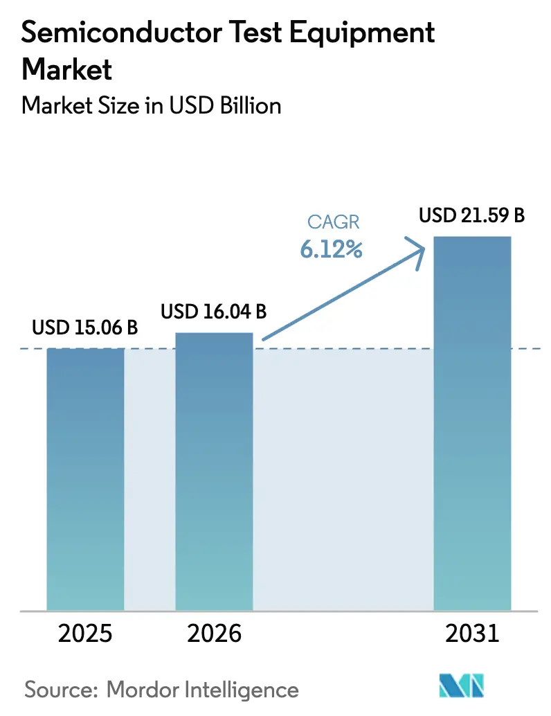
| Market Size (2026) | USD 16.04 Billion |
| Market Size (2031) | USD 21.59 Billion |
| Growth Rate (2026 - 2031) | 6.12% CAGR |
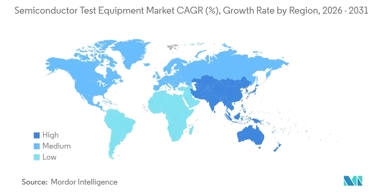
| Fastest Growing Market | Asia Pacific |
| Largest Market | Asia Pacific |
| Market Concentration | High |
Major Players *Disclaimer: Major Players sorted in no particular order Image © Mordor Intelligence. Reuse requires attribution under CC BY 4.0. | |
Semiconductor Test Equipment Market Analysis by Mordor Intelligence
The semiconductor test equipment market size was valued at USD 15.06 billion in 2025 and estimated to grow from USD 16.04 billion in 2026 to reach USD 21.59 billion by 2031, at a CAGR of 6.12% during the forecast period (2026-2031). Three forces define this trajectory: automotive electrification that raises functional-safety test requirements, migration to 3 nanometer and finer nodes that push pin counts past 10,000 channels, and the rise of chiplet-based heterogeneous integration that shifts validation from die-level to system-level. Together they lift capital intensity, widen the performance gap between legacy and advanced platforms, and draw new service models into the semiconductor test equipment market. Foundries remain the largest spenders, yet automotive tier-1 suppliers constitute the quickest-growing buyer set, reshaping equipment road maps faster than consumer electronics once did. Meanwhile, geographic demand continues to cluster in Asia-Pacific even as Southeast Asia emerges as the most agile expansion arena.
Key Report Takeaways
- By product type, automated test equipment led with 70.19% of the semiconductor test equipment market share in 2025, while probe equipment is projected to expand at a 6.57% CAGR through 2031.
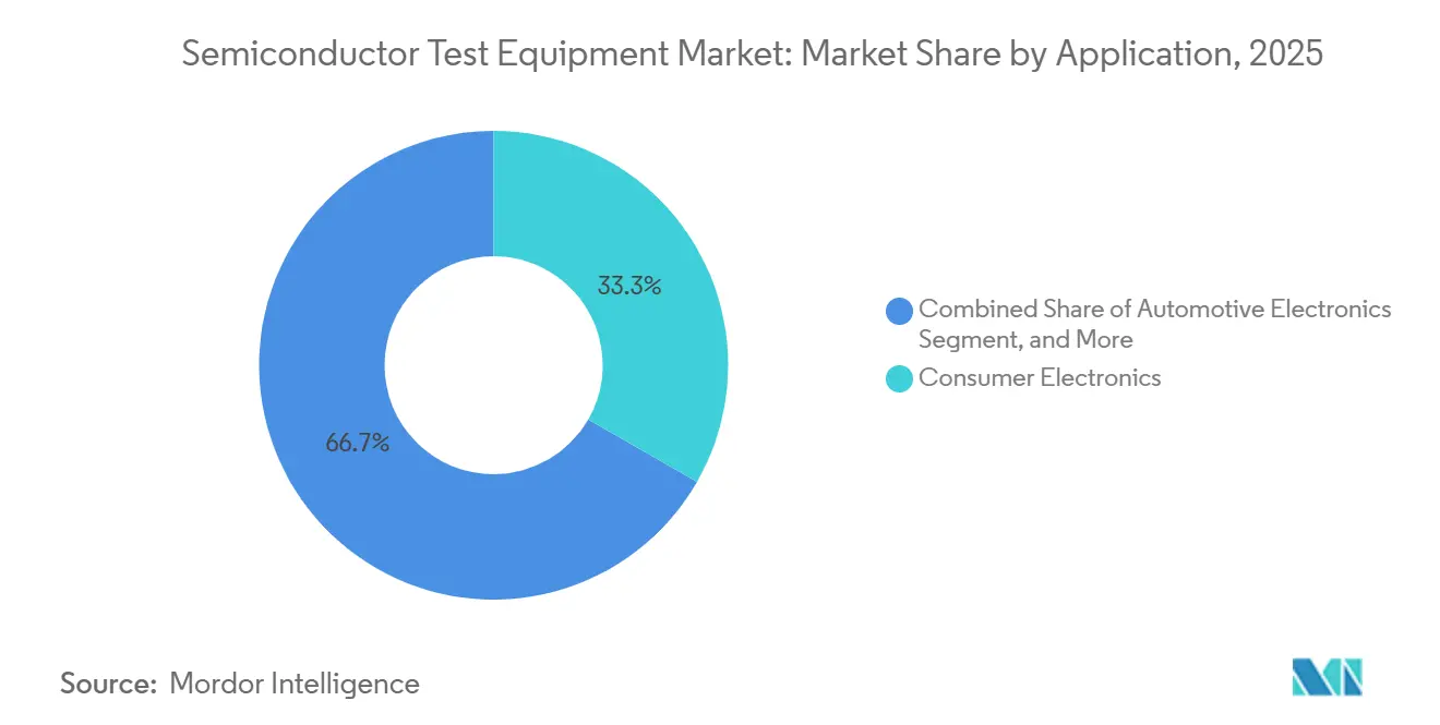
- By application, consumer electronics accounted for 33.29% of 2025 deployments, but automotive electronics testing is accelerating at a 6.91% CAGR to 2031.
- By end-use industry, foundries captured 41.21% of 2025 spending and automotive tier-1 suppliers are advancing at a 6.63% CAGR between 2026-2031.
- By geography, Asia-Pacific commanded 60.74% of the 2025 installed base, whereas Southeast Asia hubs are rising at a 6.77% CAGR over the same horizon.
Note: Market size and forecast figures in this report are generated using Mordor Intelligence’s proprietary estimation framework, updated with the latest available data and insights as of 2026.
Global Semiconductor Test Equipment Market Trends and Insights
Drivers Impact Analysis*
| Driver | (~) % Impact on CAGR Forecast | Geographic Relevance | Impact Timeline |
|---|---|---|---|
| AI-driven yield analytics accelerating parallel test coverage | +1.20% | Global, with early adoption in Taiwan, South Korea, United States | Medium term (2-4 years) |
| Automotive functional-safety mandates for ADAS and EV platforms | +1.50% | Global, strongest in Europe, North America, China | Long term (≥ 4 years) |
| Scaling of 3 nm and below nodes requiring ultra-high pin-count testers | +1.80% | Asia-Pacific core (Taiwan, South Korea), spillover to United States | Short term (≤ 2 years) |
| Heterogeneous chiplet integration creating new system-level test demand | +1.00% | Global, led by United States, Taiwan, Japan | Medium term (2-4 years) |
| OSAT capacity expansion in Southeast Asia hubs | +0.90% | Southeast Asia (Vietnam, Malaysia, Thailand) | Medium term (2-4 years) |
| Pay-per-use cloud test infrastructure models for fabless firms | +0.50% | Global, strongest uptake in North America, Europe | Short term (≤ 2 years) |
| Source: Mordor Intelligence | |||
AI-Driven Yield Analytics Accelerating Parallel Test Coverage
Machine-learning classifiers trained on terabytes of wafer-sort data now predict parametric outliers with 92% accuracy before final test, allowing test houses to route suspect die directly to extended burn-in and skip redundant measurements on known-good units.[1]J. Brown, “2-nm Era Raises Pin-Count Bar,” IEEE International Test Conference, ieee.org Advantest’s EXA Scale platform embeds convolutional neural networks that examine test-insertion loss across 512 channels in real time and cut multisite test time by 18% while maintaining defect-per-million rates below 10.[2]“Press Releases,” Advantest Corporation, advantest.com These gains let foundries amortize tester cost over higher throughput exactly when automated systems exceed USD 10 million apiece. Parallel test coverage climbs logarithmically with the sophistication of adaptive algorithms that allocate resources based on inline feedback, and early adopters report 25% reductions in cost per test after deploying reinforcement-learning agents that optimize bin limits and sequence flows without human intervention.
Automotive Functional-Safety Mandates for ADAS and EV Platforms
ISO 26262 Automotive Safety Integrity Level D rules compel tier-1 suppliers to demonstrate systematic coverage above 99.9% for microcontrollers governing brake-by-wire and battery-management functions. Test houses must now inject transient voltage spikes, single-event upsets, and thermal-runaway scenarios that consumer devices rarely encounter, which drives demand for mixed-signal testers with programmable supplies offering sub-millivolt resolution.[3]“Investor Relations,” Teradyne Inc., teradyne.com Electric vehicles integrate silicon-carbide power modules rated at 1,200 volts and 200 °C junction temperature, requiring burn-in ovens with closed-loop control and high-current probe cards capable of 400 ampere handling. The EU General Safety Regulation that came into force in 2024 further mandates advanced emergency braking and lane-keeping assist, cascading these sensor-fusion validation needs into semiconductor test specifications.[4]“General Safety Regulation,” European Commission, ec.europa.eu Consequently, qualification test time doubles versus commercial-grade parts and elevates automotive influence within the semiconductor test equipment market.
Scaling of 3 nm and Below Nodes Requiring Ultra-High Pin-Count Testers
Taiwan Semiconductor Manufacturing Company entered 2 nanometer production in late 2024 using gate-all-around FETs that tighten threshold-voltage windows to ±20 millivolts. Tester makers replied with platforms holding 12,288 pins, 32 GHz pattern generators, and femtoampere-resolution source-measure units, which pushed per-system prices beyond USD 15 million. High-bandwidth memory stacks for AI accelerators run at 6.4 Gb/s per pin, exposing crosstalk that only sub-picosecond jitter control can reveal. Moving from 5 nm to 3 nm increased wafer-sort time by 40% and raised probe card cost to as much as 12% of total test spend because cantilevers must preserve sub-5 µm planarity across 300 mm wafers. These realities amplify capital needs yet ensure revenue growth for the semiconductor test equipment market as each node shrink triggers a fresh round of system upgrades.
Heterogeneous Chiplet Integration Creating New System-Level Test Demand
The Universal Chiplet Interconnect Express (UCIe) standard ratified in 2024 enables 32 GT/s die-to-die links that stitch compute, I/O, and memory tiles from multiple fabs into a single package. Die-level tests cannot verify interposer signal integrity, thermal coupling, or power-network impedance across divergent voltage domains, so vendors are rolling out system-level platforms that stimulate every chiplet simultaneously while logging link training, ECC events, and thermal throttling. Teradyne added multi-site system-level capacity to its UltraFLEX line in 2025, enabling workloads that mirror AI inference, cryptographic hashing, or video transcoding to run during validation. Although package-level insertion adds USD 2-5 per unit, hyperscale operators accept the premium because unplanned downtime can cost USD 10,000 an hour. As chiplet architectures proliferate, system-level test moves from niche to mainstream, expanding the semiconductor test equipment market.
Restraints Impact Analysis*
| Restraint | (~) % Impact on CAGR Forecast | Geographic Relevance | Impact Timeline |
|---|---|---|---|
| Rising capex intensity amid ASP compression | -1.30% | Global, most acute in China, Southeast Asia | Short term (≤ 2 years) |
| Supply-chain bottlenecks in MEMS probe cards and burn-in sockets | -0.90% | Global, concentrated in Asia-Pacific supply base | Medium term (2-4 years) |
| Acute shortage of RF test algorithm engineers | -0.60% | Global, particularly North America, Europe | Medium term (2-4 years) |
| Escalating sustainability compliance costs | -0.40% | Europe, North America, with spillover to Asia-Pacific | Long term (≥ 4 years) |
| Source: Mordor Intelligence | |||
Rising Capex Intensity Amid ASP Compression
Average selling prices for high-performance automated testers climbed from USD 6.8 million in 2023 to USD 7.6 million in 2025, a 12% jump driven by femtoampere source-measure units and 32 GHz pattern generators. Simultaneously, chip ASPs slipped 8% as yield gains filtered into pricing, squeezing per-die budgets at outsourced assembly and test providers. Smaller subcontractors lack balance-sheet capacity to finance USD 50 million purchase orders, ceding share to large integrated manufacturers. The result is a scissors effect that drags margins and forces longer depreciation cycles, tempering the otherwise robust outlook for the semiconductor test equipment market.
Supply-Chain Bottlenecks in MEMS Probe Cards and Burn-In Sockets
Rhodium-plated cobalt-tungsten probe tips face supply concentration, with 80% of global rhodium output tied to South African mines, sending spot prices from USD 4,000/oz in 2023 to USD 12,000/oz in 2025. Lead times for high-density probe cards lengthened from 12 to 20 weeks because the two leading vendors hold 65% share and cannot parallelize micro-assembly processes. Burn-in sockets for silicon-carbide devices require high-temperature polymer insulators supplied by a handful of Japanese firms, creating additional choke points. These shortages delay product introductions by up to six weeks and inflate working capital, moderating growth in the semiconductor test equipment market.
*Our forecasts treat driver/restraint impacts as directional, not additive. The impact forecasts reflect baseline growth, mix effects, and variable interactions.
Segment Analysis
By Product Type: Automated Test Equipment Dominance Persists Amid Probe Equipment Acceleration
Automated test equipment claimed 70.19% of 2025 revenue, underscoring its role as the primary workhorse across logic, memory, and mixed-signal validation. The semiconductor test equipment market size attributed to this category is projected to keep expanding because every new process node demands higher bandwidth, finer timing resolution, and broader power fidelity. Probe equipment is advancing at a 6.57% CAGR through 2031, fuelled by wafer-level test intensity that rises with node scaling and chiplet demands. Burn-in systems continue to serve safety-critical verticals such as automotive microcontrollers and aerospace FPGAs, while handler equipment benefits from labour-cost arbitrage in Vietnam and Malaysia where robotized pick-and-place reduces manual touchpoints.
Optical inspection systems now embed deep-learning classifiers capable of spotting sub-10 nm defects, a function increasingly critical as advanced packaging introduces micro-bumps and through-silicon vias. Hybrid platforms are emerging that blur old boundaries: automated test equipment vendors add package-level stimulus, and probe-station suppliers integrate functional modules. Collectively, these shifts reinforce the semiconductor test equipment market as an ecosystem where adjacent categories increasingly converge instead of remaining siloed.


By Application: Wafer-Sort and System-Level Test Gain Prominence
Wafer-sort and probe test absorbs 40% of total test budgets because early identification of parametric outliers prevents expensive packaging waste, especially when probe cards can cost USD 500,000 apiece. Final test still represents 35% of spending, validating timing margins and power under workload stress. System-level test holds 15% today but grows at double-digit rates as chiplet-based designs multiply, signalling a new revenue layer inside the semiconductor test equipment market. Reliability and burn-in, once 20% of budgets, has receded to 10% because statistical process control captures many latent failures earlier in the flow.
Consumer electronics dominate test volumes, yet automotive, industrial, and 5G infrastructure applications impose more stringent protocols that lengthen every test sequence. As these mission-critical domains expand, system-level and stress-oriented tests reclaim budget share, boosting the semiconductor test equipment market share for vendors able to bundle functional, thermal, and radio-frequency capabilities in one platform.
By End-Use Industry: Foundries Command Share While Automotive Tier-1s Drive Growth
Foundries accounted for 41.21% of 2025 outlays, reflecting the capital intensity of advanced fabs where 8-10% of total tool spend flows to test and metrology. Consequently, the semiconductor test equipment market size aligned with foundry demand is forecast to rise in lockstep with each new process ramp. Automotive tier-1s, although smaller in absolute spend, are expanding fastest at a 6.63% CAGR as electrification lifts semiconductor content per vehicle from USD 600 to USD 2,000.
Consumer electronics brands contributed 25% of 2025 revenue, but lengthening replacement cycles temper growth momentum. Industrial and power applications focus on wide-bandgap devices rated beyond 1,200 volts, requiring niche burn-in and high-power testers. Telecommunications infrastructure builds around 5G and future 6G keep radio-frequency throughput demands high, whereas healthcare and life-science customers, though small, command premium pricing for traceability and regulatory compliance.
Geography Analysis
Asia-Pacific delivered 60.74% of 2025 installations on the back of Taiwan, South Korea, and mainland China operating 180 of the world’s 300 high-volume fabs. The semiconductor test equipment market resonates here because every new wafer-fab module immediately pulls in corresponding test capacity. Southeast Asia enlarges its role at a 6.77% CAGR as Amkor Technology, ASE Group, and JCET Group localize assembly and test lines in Vietnam, Malaysia, and Thailand, chasing 30% lower labour costs and geopolitical diversification. Japan’s domestic champions maintain 40% global share in radiofrequency, high-power, and cryogenic testers, reinforcing Tokyo’s strategic presence even as overall Japanese demand grows moderately.
North America supplied 18% of 2025 revenue, shaped by Intel’s foundry expansion and sustained defense spending. Fabless giants such as NVIDIA and Qualcomm influence tester specifications even without owning fabs, ensuring that U.S. design wins translate into global equipment standards. Europe held 12% with a concentration in Germany’s automotive cluster and subsidies under the EUR 43 billion Chips Act that seeks to double regional capacity by 2030. Subsidy timelines mean tangible equipment demand trails policy announcements by three to four years, yet vendors already size their road maps around the coming European fabs.
South America, the Middle East, and Africa together occupied 10% of 2025 deployments, led by Brazil’s automotive assembly lines and the United Arab Emirates’ nascent fab in Abu Dhabi. China’s internal dynamics warrant special note: domestic testers captured 25% of the local market by offering mature-node platforms at 30% discounts, prompting multinationals to localize manufacturing or accept margin compression. Export controls on sub-10 nm test technology accelerate indigenous development, reshaping long-term competitiveness inside the semiconductor test equipment market.

Competitive Landscape
Advantest, Teradyne, and Cohu collectively hold about 55% share, rendering market concentration moderate and leaving ample room for specialists in millimeter-wave, burn-in, and optical inspection niches. Incumbents pursue vertical integration to seize consumable margins: Teradyne acquired a probe-card design house in 2025, and Formfactor partnered with a MEMS foundry to shorten lead times. Chinese players such as Hangzhou Changchuan and Beijing Huafeng are moving upmarket, releasing 28 nm-capable testers and ISO 26262 modules that undercut prices by 20-30%, a trend that forces global suppliers to balance technology differentiation against cost competitiveness.
White-space opportunities emerge around system-level test for chiplet packages, where no standard platform prevails. Vendors experiment with modular architectures that blend automated tester back-ends, thermal chambers, and high-speed interposers into a single cell. Simultaneously, pay-per-use cloud test models convert USD 8 million hardware into subscription services, lowering barriers for fabless firms that launch fewer than ten designs each year. This as-a-service transition shifts revenue recognition from upfront capital sales to recurring operating income, a change that could realign valuation metrics across the semiconductor test equipment industry.
Artificial-intelligence-driven analytics represents the newest arms race. Advantest and Teradyne embed proprietary algorithms, whereas mid-tier vendors license software from third parties to close the feature gap. The next competitive frontier extends into sustainability auditing and carbon-aware scheduling, areas where European regulations already push for life-cycle assessment disclosures. Whoever master’s both AI predictive control and eco-certification is likely to capture a premium segment of the semiconductor test equipment market.
Semiconductor Test Equipment Industry Leaders
Advantest Corporation
Teradyne Inc.
Cohu Inc.
Chroma ATE Inc.
Tokyo Electron Ltd.
- *Disclaimer: Major Players sorted in no particular order

Recent Industry Developments
- August 2025: Advantest showcased its T5801 ultra-high-speed DRAM tester at Future of Memory and Storage 2025, covering GDDR7, LPDDR6, and DDR6.
- June 2025: MA-tek invested NTD 100 million (USD 3.3 million) in ultra-high-power burn-in equipment for AI chips.
- May 2025: FormFactor doubled its Taiwan service capacity, adding silicon-photonic test demos.
- April 2025: Teradyne bought 10% of Technoprobe for USD 516 million and sold its Device Interface arm for USD 85 million.


Global Semiconductor Test Equipment Market Report Scope
The Semiconductor Test Equipment Market Report is Segmented by Product Type (Automated Test Equipment, Burn-in Systems, Handler Equipment, Probe Equipment, Optical Inspection Systems, Other Equipment Categories), Application (Wafer Sort/Probe, Final Test, System-Level Test, Reliability/Burn-in), End-Use Industry (Consumer Electronics, Automotive and Mobility, Industrial and Power, Telecommunications and Networking, Healthcare and Life-Science, Other End-Use Industries), and Geography (North America, South America, Europe, Asia-Pacific, Middle East and Africa). The Market Forecasts are Provided in Terms of Value (USD).
| Automated Test Equipment (ATE) |
| Burn-in Systems |
| Handler Equipment |
| Probe Equipment |
| Optical Inspection Systems |
| Other Equipment Categories |
| Wafer Sort / Probe |
| Final Test |
| System-Level Test |
| Reliability / Burn-in |
| Consumer Electronics |
| Automotive And Mobility |
| Industrial And Power |
| Telecommunications And Networking |
| Healthcare And Life-Science |
| Other End-Use Industries |
| North America | United States | |
| Canada | ||
| Mexico | ||
| South America | Brazil | |
| Argentina | ||
| Rest Of South America | ||
| Europe | Germany | |
| United Kingdom | ||
| France | ||
| Russia | ||
| Rest Of Europe | ||
| Asia-Pacific | China | |
| Japan | ||
| India | ||
| South Korea | ||
| South-East Asia | ||
| Rest Of Asia-Pacific | ||
| Middle East And Africa | Middle East | Saudi Arabia |
| United Arab Emirates | ||
| Rest Of Middle East | ||
| Africa | South Africa | |
| Egypt | ||
| Rest Of Africa | ||
| By Product Type | Automated Test Equipment (ATE) | ||
| Burn-in Systems | |||
| Handler Equipment | |||
| Probe Equipment | |||
| Optical Inspection Systems | |||
| Other Equipment Categories | |||
| By Application | Wafer Sort / Probe | ||
| Final Test | |||
| System-Level Test | |||
| Reliability / Burn-in | |||
| By End-Use Industry | Consumer Electronics | ||
| Automotive And Mobility | |||
| Industrial And Power | |||
| Telecommunications And Networking | |||
| Healthcare And Life-Science | |||
| Other End-Use Industries | |||
| By Geography | North America | United States | |
| Canada | |||
| Mexico | |||
| South America | Brazil | ||
| Argentina | |||
| Rest Of South America | |||
| Europe | Germany | ||
| United Kingdom | |||
| France | |||
| Russia | |||
| Rest Of Europe | |||
| Asia-Pacific | China | ||
| Japan | |||
| India | |||
| South Korea | |||
| South-East Asia | |||
| Rest Of Asia-Pacific | |||
| Middle East And Africa | Middle East | Saudi Arabia | |
| United Arab Emirates | |||
| Rest Of Middle East | |||
| Africa | South Africa | ||
| Egypt | |||
| Rest Of Africa | |||


Key Questions Answered in the Report
What is the projected revenue for the semiconductor test equipment market in 2031?
The semiconductor test equipment market size is forecast to reach USD 21.59 billion by 2031.
Which product type currently dominates spending?
Automated test equipment captured 70.19% of 2025 revenue, making it the largest product category.
Why is probe equipment growing faster than other segments?
Probe equipment benefits from node scaling and chiplet architectures that intensify wafer-level screening, driving a 6.57% CAGR through 2031.
Which region is expected to expand most rapidly?
Southeast Asia is advancing at a 6.77% CAGR as OSAT providers relocate capacity to Vietnam, Malaysia, and Thailand.
How will automotive trends influence demand?
ISO 26262 safety mandates and higher semiconductor content per vehicle push automotive tier-1 suppliers test spending at a 6.63% CAGR from 2026-2031.
What competitive pressure do incumbents face from China?
Domestic Chinese vendors offer mature-node testers at 20-30% lower prices, forcing global suppliers to localize or accept margin compression.
Page last updated on:


