Semiconductor Back-End Equipment Market Size and Share
Market Overview
| Study Period | 2019 - 2030 |
|---|---|
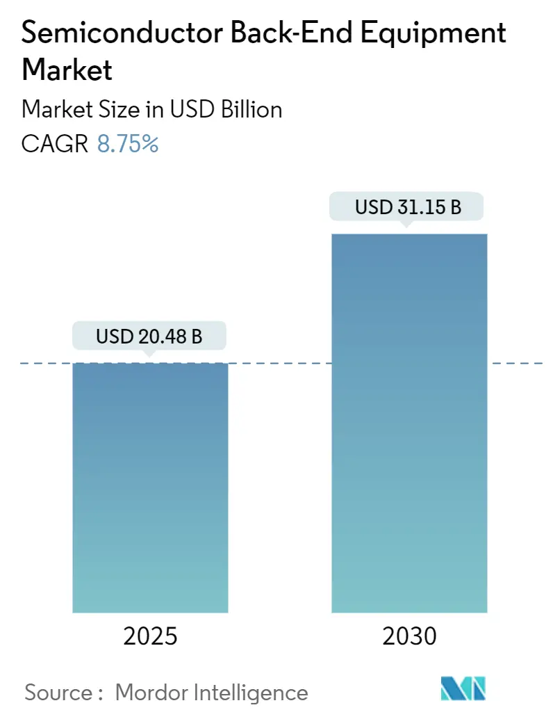
| Market Size (2025) | USD 20.48 Billion |
| Market Size (2030) | USD 31.15 Billion |
| Growth Rate (2025 - 2030) | 8.75% CAGR |
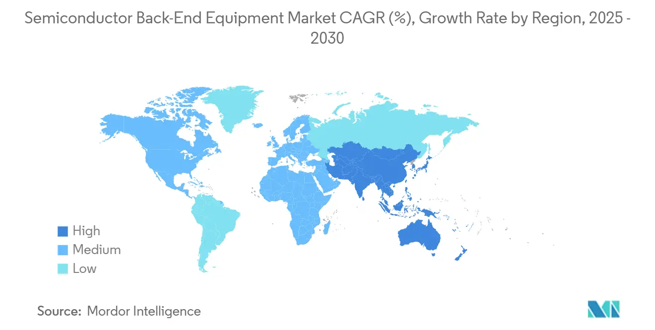
| Fastest Growing Market | Asia Pacific |
| Largest Market | Asia Pacific |
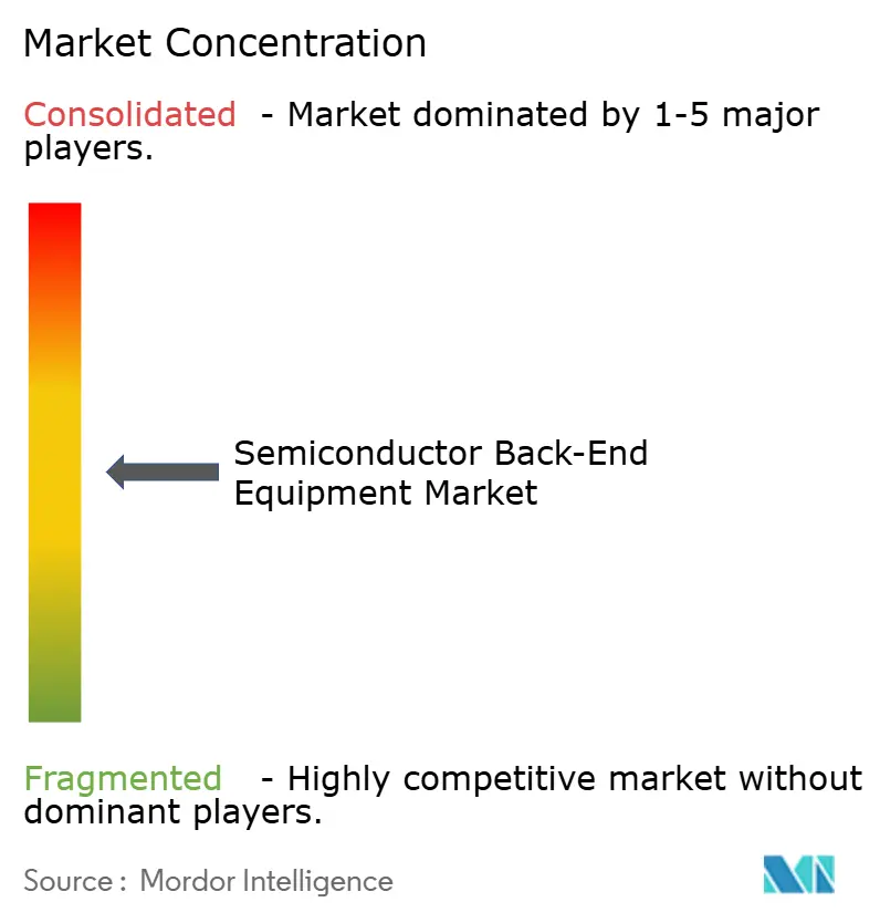
| Market Concentration | Medium |
Major Players *Disclaimer: Major Players sorted in no particular order Image © Mordor Intelligence. Reuse requires attribution under CC BY 4.0. | |
Semiconductor Back-End Equipment Market Analysis by Mordor Intelligence
The semiconductor back-end equipment market size stands at a USD 20.48 billion market size in 2025 and is projected to reach USD 31.15 billion by 2030, delivering an 8.75% CAGR over the forecast period. Robust demand for advanced packaging that supports artificial intelligence and high-performance computing continues to redefine assembly, bonding, and test requirements. Precision hybrid-bonding, wafer-level burn-in, and laser lift-off tools are now pivotal as chipmakers migrate from monolithic system-on-chip designs to multi-die architectures with high-bandwidth memory stacking. Regional build-outs of foundry capacity in Taiwan, South Korea, and mainland China, together with North American and European incentive schemes, are intensifying the purchasing cycle for cutting-edge assembly gear. Export-control limits on China and a persistent packaging-engineering talent shortage act as structural drags but have not derailed overall equipment demand, particularly for wafer-level back-end processes.
Key Report Takeaways
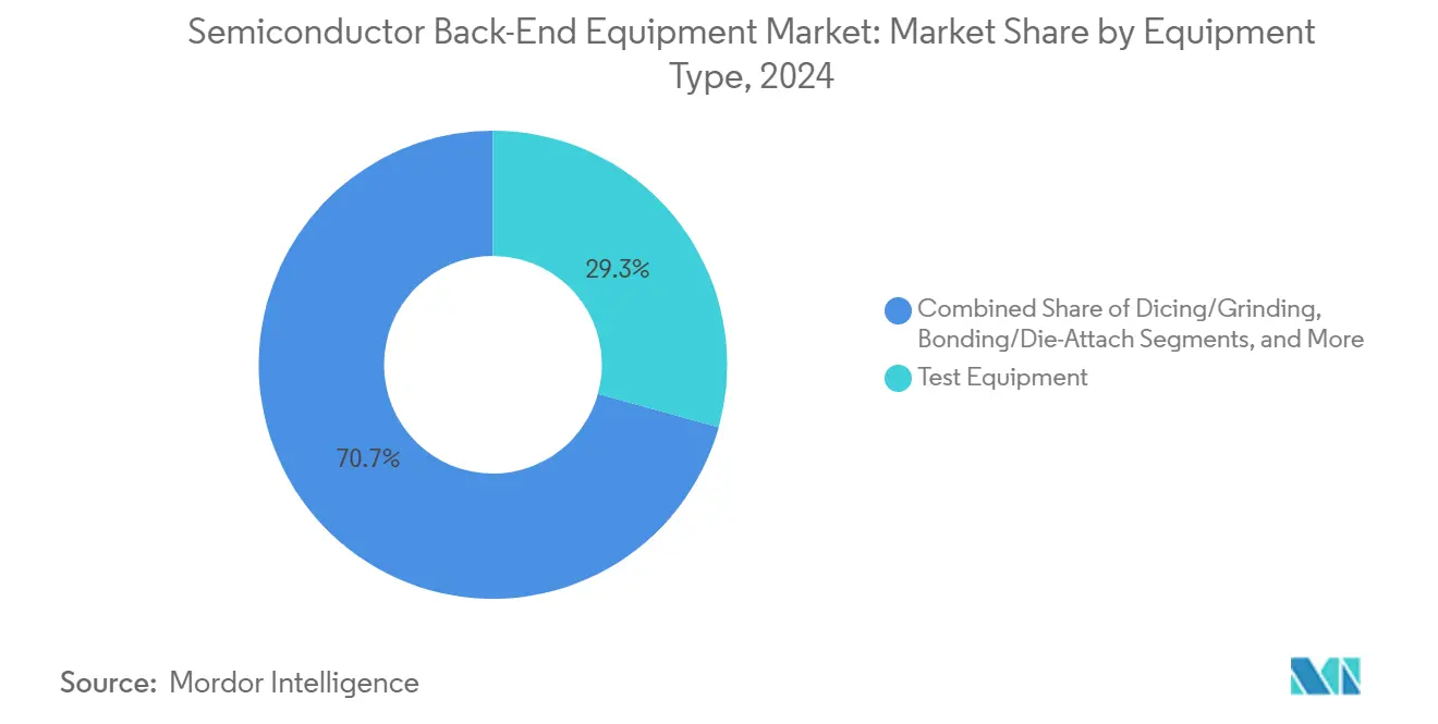
- By equipment type, test equipment led with 29.3% semiconductor back-end equipment market share in 2024, while assembly and packaging tools recorded a 9.9% CAGR to 2030.
- By process stage, the final test stage accounted for 39.7% of the semiconductor back-end equipment market size in 2024, whereas the wafer-level back-end stage is forecast to compound at a 10.3% CAGR through 2030.
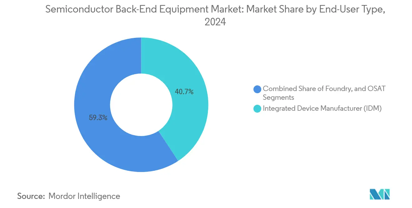
- By end-user type, IDMs controlled 40.7% of 2024 revenue, yet the OSAT segment is expanding at a 10.2% CAGR to 2030.
- By application industry, consumer electronics captured 26.2% of 2024 revenue, but automotive and mobility devices are advancing at a 9.7% CAGR through 2030.
- By geography, Asia-Pacific held 60.1% revenue share in 2024 and is expected to grow at a 10.5% CAGR to 2030.
Global Semiconductor Back-End Equipment Market Trends and Insights
Drivers Impact Analysis*
| DRIVER | (~) % IMPACT ON CAGR FORECAST | GEOGRAPHIC RELEVANCE | IMPACT TIMELINE |
|---|---|---|---|
| Surging demand for advanced packaging for AI/HPC | +2.8% | Global, concentrated in Asia-Pacific and North America | Medium term (2-4 years) |
| Expansion of semiconductor content in EVs | +1.9% | Global, early gains in China, Europe, North America | Long term (≥ 4 years) |
| Government incentive programmes (CHIPS-Act, EU-Chips) | +1.6% | North America, Europe with global spillover | Medium term (2-4 years) |
| Foundry capacity buildouts in Asia | +1.4% | Asia-Pacific core with global spillover | Short term (≤ 2 years) |
| Adoption of wafer-level burn-in for AI accelerators | +0.9% | Global, focused in advanced foundry sites | Short term (≤ 2 years) |
| Heterogeneous integration needing adaptive die-attach | +0.7% | Global, leading-edge manufacturing hubs | Medium term (2-4 years) |
| Source: Mordor Intelligence | |||
Surging Demand for Advanced Packaging for AI and HPC
Advanced packaging now dictates back-end equipment purchasing as high-bandwidth memory integration becomes mandatory for next-generation graphics and server processors. TSMC is ramping panel-level packaging lines to support volume production for leading cloud providers, enabling higher die density and improved thermal paths. Applied Materials forecasts more than USD 600 million in fiscal-year 2024 revenue from HBM-specific equipment, leveraging over 50% share in DRAM wafer processing gear. Wafer-level burn-in tools such as Aehr Test Systems’ FOX-XP platform enable simultaneous stress screening of dozens of AI accelerators at elevated temperature, shortening validation cycles and bolstering overall reliability. Demand for hybrid-bonding align-and-attach modules continues to rise because they form low-resistance copper-to-copper interconnects essential for HBM4 stacks running above 5 TB/s bandwidth. As a result, both materials engineering firms and niche bonding specialists are securing long-term purchase agreements with logic and memory makers.
Expansion of Semiconductor Content in EVs
Electric-vehicle manufacturers rely on silicon-carbide and gallium-nitride devices that tolerate 200 °C junction temperatures and switch at high voltages with minimal losses. Specialized back-end equipment now incorporates high-pressure sintering, advanced fluxless thermal-compression bonding, and wafer-clean systems such as the SCREEN SS-3200 that remove contamination prior to high-temperature anneal. Leading automotive OEMs, including Tesla and Hyundai, already deploy SiC MOSFET inverters, driving OSAT investment in high-reliability package formats qualified for 15-year lifetimes. These stringent requirements push equipment suppliers to prioritize void-free die-attach, automated X-ray inspection, and active thermal-cycling capabilities.
Government Incentive Programs
The USD 39 billion CHIPS Act and EUR 43 billion (USD 50.34 billion) EU Chips Act provide matching funds, tax credits, and workforce grants that de-risk capital spending on domestic assembly and testing lines. The European Chips Act has unlocked more than EUR 80 billion (USD 93.65 billion) of combined public-private investment, including advanced packaging pilot lines in Germany, France, and Italy.[1]Source: European Commission, “European Chips Act – Update on the latest milestones,” europa.eu Entegris secured USD 75 million in CHIPS funding to build a Colorado Springs pod and filtration plant, generating 600 jobs and localizing key consumables production.[2]Source: Entegris, “Entegris and Biden Administration Announce up to USD 75 Million in Proposed Direct Funding Under CHIPS Act,” entegris.com Applied Materials’ planned USD 400 million collaborative engineering center in Bangalore underscores how incentives are spurring regional research and development hubs that will consume next-generation back-end tools. Such policy support reduces geographic concentration risk and underwrites multi-year procurement roadmaps for equipment vendors.
Foundry Capacity Buildouts in Asia
Leading pure-play foundries are enlarging advanced packaging footprints to complement front-end node shrink. TSMC’s first 2 nm risk production uses gate-all-around devices that require precision bonding and wafer-level reliability testing, fueling near-term tool deliveries. Samsung aims to quadruple its advanced-package output by 2028 and diversify away from standard wafer-bumping into chiplet-based interposers. SEMI projects global fab capacity will top 42.5 million wafers per quarter by end-2025, with mainland China still adding lines despite export restraints.[3]Source: SEMI, “300 mm Fab Equipment Spending Forecast to Reach Record USD 137 Billion in 2027,” semi.org To capture the surge, Tokyo Electron is spending JPY 104 billion (USD 0.71 billion) on a smart-production building in Miyagi that triples shipment throughput while lowering energy per tool shipped. These supply-chain expansions shorten shipping lead-times and anchor long-run demand for inspection, metrology, and laser-debonding systems.
Restraints Impact Analysis*
| RESTRAINTS | (~) % IMPACT ON CAGR FORECAST | GEOGRAPHIC RELEVANCE | IMPACT TIMELINE |
|---|---|---|---|
| High capital outlay and long ROI | -1.8% | Global, more severe in emerging markets | Long term (≥ 4 years) |
| Rapid technology cycles cause tool obsolescence | -1.3% | Global, concentrated in leading-edge fabs | Short term (≤ 2 years) |
| Shortage of skilled packaging engineers | -1.1% | Acute in Asia-Pacific and North America | Medium term (2-4 years) |
| Export-control limits on China tool shipments | -0.9% | China and supplier nations | Medium term (2-4 years) |
| Source: Mordor Intelligence | |||
High Capital Outlay and Long ROI
Single hybrid-bonding clusters can cost more than USD 40 million, often surpassing the balance-sheet capacity of second-tier OSATs. When demand pauses, utilization rates fall below the 70% break-even threshold, extending payback periods beyond five years. Tokyo Electron trimmed its fiscal-2025 profit outlook by 18% as memory makers pushed out deliveries, illustrating how volatile purchase cycles translate into earnings swings. Smaller IDMs in emerging regions hesitate to adopt the latest die-attach or plasma-clean systems until anchor customers commit volume, slowing technology diffusion.
Shortage of Skilled Packaging Engineers
The global semiconductor sector must add more than 160,000 skilled workers in the United States alone by 2032 to sustain advanced packaging roadmaps. Taiwan’s packaging houses require an additional 34,000 technicians to run newly installed lines.[4]Source: Taipei Times, “Semiconductor industry faces 34,000-worker shortage amid rapid expansion,” taipeitimes.com High employee turnover, measured at 53% intention to switch jobs, forces OSATs to increase automation or risk sub-optimal tool utilization. Education pipelines struggle to update curricula on topics such as under-bump metallization chemistry, thermal interface material characterization, and machine vision alignment, thereby prolonging the skilled labor bottleneck.
*Our forecasts treat driver/restraint impacts as directional, not additive. The impact forecasts reflect baseline growth, mix effects, and variable interactions.
Segment Analysis
By Equipment Type: Test Gear Retains Leadership Yet Packaging Tools Accelerate
Test systems generated 29.3% of revenue of semiconductor back-end equipment market share in 2024, reflecting the escalating complexity of AI accelerators that demand loop-back memory test, high-speed SerDes characterization, and wafer-level burn-in. Advantest again ranked first in the TechInsights customer-satisfaction survey, thanks to partnerships with FormFactor and Technoprobe that expand probe-card ecosystem support. At the same time, assembly and packaging tools are forecast to expand at a 9.9% CAGR, the highest among all equipment categories, as hybrid bonding migrates from pilot to high-volume manufacturing. Applied Materials and BE Semiconductor Industries’ co-developed platforms have already booked multi-tool orders at leading logic fabs. Metrology and inspection tools also see outsized demand because heterogeneous integration multiplies defect-locate points; Onto Innovation posted record revenue on AI-packaging scan demand.
While dicing and grinding gear faces commoditization, Disco’s double-rotary technology attracts buyers seeking low-chipping saws for stacked-die memory. Laser lift-off systems, such as Tokyo Electron’s Ulucus LX, decrease debond cycle time and reduce deionized water use by 90%, a sustainability differentiator. Overall, value capture shifts from mature back-grind or pick-and-place modules to high-precision bond aligners, fine-pitch probe stations, and integrated metrology-during-bond elements that safeguard yield for 3 µm interconnect pitch.


By Process Stage: Wafer-Level Back-End Gains Momentum
The final-test stage retained 39.7% semiconductor back-end equipment market share in 2024 on the strength of established burn-in, automatic test, and system board test lines. Nevertheless, wafer-level back-end tools are forecast to climb at a 10.3% CAGR, outpacing other stages as builders seek to detect latent defects earlier in the flow. SEMI reported a surge in wafer-level burn-in chambers, ultraviolet curing ovens, and plasma activation modules, driven by AI workloads that cannot tolerate early field failures. Tokyo Electron’s smart-fab project streamlines wafer-level logistics, embedding automated guided vehicles and real-time analytics to maintain ±1 °C process-window stability across laser lift-off and cleaning cells.
By bringing high-stress screening and optical-die-shift inspection upstream, fabs minimize yield-loss propagation into expensive package finishes. However, wafer-level adoption requires coordinated recipe integration across metrology, wet clean, bonding, and test modules to avoid bottlenecks. Integrated device houses thus favor turnkey clusters over discrete tool buys, allocating unified budgets that blend front-end and back-end capital lines to gain holistic throughput gains.
By End-User Type: OSAT Growth Outpaces IDM Spend
IDMs in semiconductor back-end equipment market represented 40.7% market share in 2024 but are expected to cede unit share as fab-lite suppliers outsource assembly to large OSATs. ASE’s acquisition of Infineon’s packaging lines in the Philippines and South Korea underpins a strategy to hold broader module capability spanning power, MEMS, and advanced system-in-package formats. As more fabless AI chip startups move from prototype to volume, they purchase turnkey assembly and test slots rather than financing in-house lines, prompting OSATs to order panel-level bonder clusters, sinter presses, and fan-out redistribution tools.
Foundries are another high-growth buyer group, using advanced packaging as a margin stabilizer while wafer-price erosion continues at mature nodes. TSMC’s CoWoS capacity addition requires multi-chamber hybrid-bond lines alongside high-density interposer builds, driving front-to-back capital coordination. The competition between IDMs, foundries, and OSATs is blurring as each invests in overlapping capabilities to secure turnkey AI chiplet programs.
By Application Industry: Automotive Pulls Ahead of Consumer Electronics
Consumer electronics retained 26.2% of 2024's semiconductor back-end equipment market revenue, but its mid-single-digit unit growth is overshadowed by the automotive and mobility category, which is projected to chart a 9.7% CAGR through 2030. Electric vehicles increasingly integrate 5 nm domain controllers, mmWave radar, lidar, and high-efficiency power modules, all of which rely on advanced substrate technologies. Power chips built on SiC or GaN require silver-sinter die attach and liquid-cool packages that withstand 1,500 thermal cycles, pushing OSATs toward vacuum reflow and in-line X-ray metrology.
Data-center and high-performance computing devices likewise demand wafer-level burn-in and cryogenic etch tools to support interconnect pitches under 5 µm and operating temperatures reaching 85 °C in stacked DRAM modules. Industrial IoT devices, while smaller in volume, require ruggedized fan-out packages for edge analytics under harsh settings. Each application brings distinctive material and process specifications, widening the menu of tool types that back-end suppliers must support.
Geography Analysis
Asia-Pacific accounted for a 60.1% semiconductor back-end equipment market share in 2024 and is forecast to log a 10.5% CAGR through 2030. Taiwan alone supports nearly half of global IC packaging capacity, and local OSATs continue to expand micro-LED panel-level pilot lines that demand sub-1 µm bonding accuracy. Mainland China raised semiconductor equipment purchases 29% year-over-year in 2023 to USD 36.6 billion despite U.S. export limits, buoyed by domestic subsidies that prioritize assembly and testing gear unencumbered by extreme ultraviolet restrictions. South Korea’s equipment investment slipped, yet SK hynix and Samsung both increased flip-chip ball-grid-array throughput for HBM 3E memory stacks, sustaining a baseline for test handler and memory-probe demand.
North America benefits directly from the CHIPS Act and now houses new back-end campuses in Arizona, Texas, and New York. SEMI calculates that regional spending rose 15% in 2024 and could reach USD 24.7 billion by 2027 as tier-one IDMs add advanced packaging lines co-located with front-end fabs. Europe added 3% spending in 2024, backed by the EU Chips Act, but remains capacity-limited; new facilities in Dresden and Crolles are not expected to complete tool move-in until late 2026.
The Middle East and Africa, while nascent, attract pilot back-end operations in Dubai and Israel, and India’s production-linked incentive scheme has drawn commitments from both assembly contractors and equipment OEMs. Regional diversification moderates supply chain risk and opens incremental demand pockets for localized equipment service contracts.

Competitive Landscape
Applied Materials has secured a substantial stake in HBM-specific deposition and etch systems, while Tokyo Electron holds a strong foothold in the coater-developer module, pivotal for general back-end lithography. Nova’s USD 60 million acquisition of Sentronics Metrology extends its dimensional-metrology reach into wafer-level packaging, targeting a USD 200 million addressable revenue pool.
Artificial-intelligence-driven software now differentiates hardware; Chroma ATE reduced handler-software migration time from 140 hours to 5 hours by embedding predictive algorithms, thereby lowering customers’ line conversion costs. Sustainability features also matter: Tokyo Electron’s cryogenic etch option cuts process CO₂ by 80% and water use by 70%, winning bids with clients that have science-based emission targets. Export controls have reshuffled the share, enabling domestic Chinese vendors to win sockets previously awarded to U.S. firms. Meanwhile, Japanese suppliers such as Nikon pioneered direct-write digital lithography for back-end substrates up to 600 mm square, enabling high-throughput panel packaging orders that mature OSATs view as a route to cost scaling.
Consolidation is moderate, with the top five suppliers controlling roughly 65% of revenue. Yet white-space opportunities persist in panel-level glass-substrate handling, adaptive compression bonding, and wafer-level hermetic encapsulation for wide-bandgap power modules. As hybrid bonding migrates down-node, incumbent lithography, deposition, and etch suppliers are likely to deepen vertical integration, further concentrating capabilities at the interface between front- and back-end.
Semiconductor Back-End Equipment Industry Leaders
Advantest Corporation
ASMPT Limited
Teradyne, Inc.
Disco Corporation
Kulicke & Soffa Industries, Inc.
- *Disclaimer: Major Players sorted in no particular order


Global Semiconductor Back-End Equipment Market Report Scope
The semiconductor back-end equipment market study tracks the revenue accrued through the sale of semiconductor back-end equipment by various players in the global market. The study also tracks the key market parameters, underlying growth influencers, and major vendors operating in the industry, which supports the market estimation and growth rates over the forecast period. The study further analyzes the overall impact of COVID-19 aftereffects and other macroeconomic factors on the market. The report’s scope encompasses market sizing and forecasts for the various market segments.
The Semiconductor Back-End Equipment Market Report is Segmented by Equipment Type (Metrology and Inspection, Dicing/Grinding, Bonding/Die-Attach, Assembly and Packaging Tools, and Test Equipment), Process Stage (Wafer-Level Backend, Assembly and Packaging Stage, and Final Test Stage), End-User Type (IDM, Foundry, OSAT), Application Industry (Consumer Electronics, Automotive and Mobility, Data-Center and HPC, and Industrial and IoT), and Geography (North America, South America, Asia-Pacific, Europe, and Middle East and Africa). The Market Forecasts are Provided in Terms of Value (USD).
| Metrology and Inspection |
| Dicing/Grinding |
| Bonding/Die-Attach |
| Assembly and Packaging Tools |
| Test Equipment |
| Wafer-Level Backend |
| Assembly and Packaging Stage |
| Final Test Stage |
| Integrated Device Manufacturer (IDM) |
| Foundry |
| Outsourced Semiconductor Assembly and Test (OSAT) |
| Consumer Electronics |
| Automotive and Mobility |
| Data-Center and HPC |
| Industrial and IoT |
| North America | United States | |
| Canada | ||
| Mexico | ||
| South America | Brazil | |
| Argentina | ||
| Rest of South America | ||
| Europe | Germany | |
| United Kingdom | ||
| France | ||
| Spain | ||
| Rest of Europe | ||
| Asia-Pacific | China | |
| Japan | ||
| India | ||
| Southeast Asia | ||
| Rest of Asia-Pacific | ||
| Middle East and Africa | Middle East | Saudi Arabia |
| United Arab Emirates | ||
| Rest of Middle East | ||
| Africa | South Africa | |
| Egypt | ||
| Rest of Africa | ||
| By Equipment Type | Metrology and Inspection | ||
| Dicing/Grinding | |||
| Bonding/Die-Attach | |||
| Assembly and Packaging Tools | |||
| Test Equipment | |||
| By Process Stage | Wafer-Level Backend | ||
| Assembly and Packaging Stage | |||
| Final Test Stage | |||
| By End-User Type | Integrated Device Manufacturer (IDM) | ||
| Foundry | |||
| Outsourced Semiconductor Assembly and Test (OSAT) | |||
| By Application Industry | Consumer Electronics | ||
| Automotive and Mobility | |||
| Data-Center and HPC | |||
| Industrial and IoT | |||
| By Geography* | North America | United States | |
| Canada | |||
| Mexico | |||
| South America | Brazil | ||
| Argentina | |||
| Rest of South America | |||
| Europe | Germany | ||
| United Kingdom | |||
| France | |||
| Spain | |||
| Rest of Europe | |||
| Asia-Pacific | China | ||
| Japan | |||
| India | |||
| Southeast Asia | |||
| Rest of Asia-Pacific | |||
| Middle East and Africa | Middle East | Saudi Arabia | |
| United Arab Emirates | |||
| Rest of Middle East | |||
| Africa | South Africa | ||
| Egypt | |||
| Rest of Africa | |||


Key Questions Answered in the Report
How large is the semiconductor back-end equipment market in 2025?
It is valued at USD 20.48 billion and is forecast to reach USD 31.15 billion by 2030.
Which region contributes most to equipment demand?
Asia-Pacific commands a 60.1% revenue share in 2024 and remains the fastest-growing geography, expanding at 10.5% CAGR.
Which equipment segment shows the fastest growth?
Assembly and packaging tools are projected to post a 9.9% CAGR through 2030, outpacing test, metrology, and dicing categories.
Why are hybrid-bonding tools important?
Hybrid bonding enables direct copper-to-copper interconnects for HBM stacks and chiplet packages, driving demand for ultra-precise aligners.
Page last updated on:


