2.5D And 3D Semiconductor Packaging Market Size and Share
Market Overview
| Study Period | 2020 - 2031 |
|---|---|
| Market Size (2026) | USD 12.73 Billion |
| Market Size (2031) | USD 24.18 Billion |
| Growth Rate (2026 - 2031) | 13.69% CAGR |
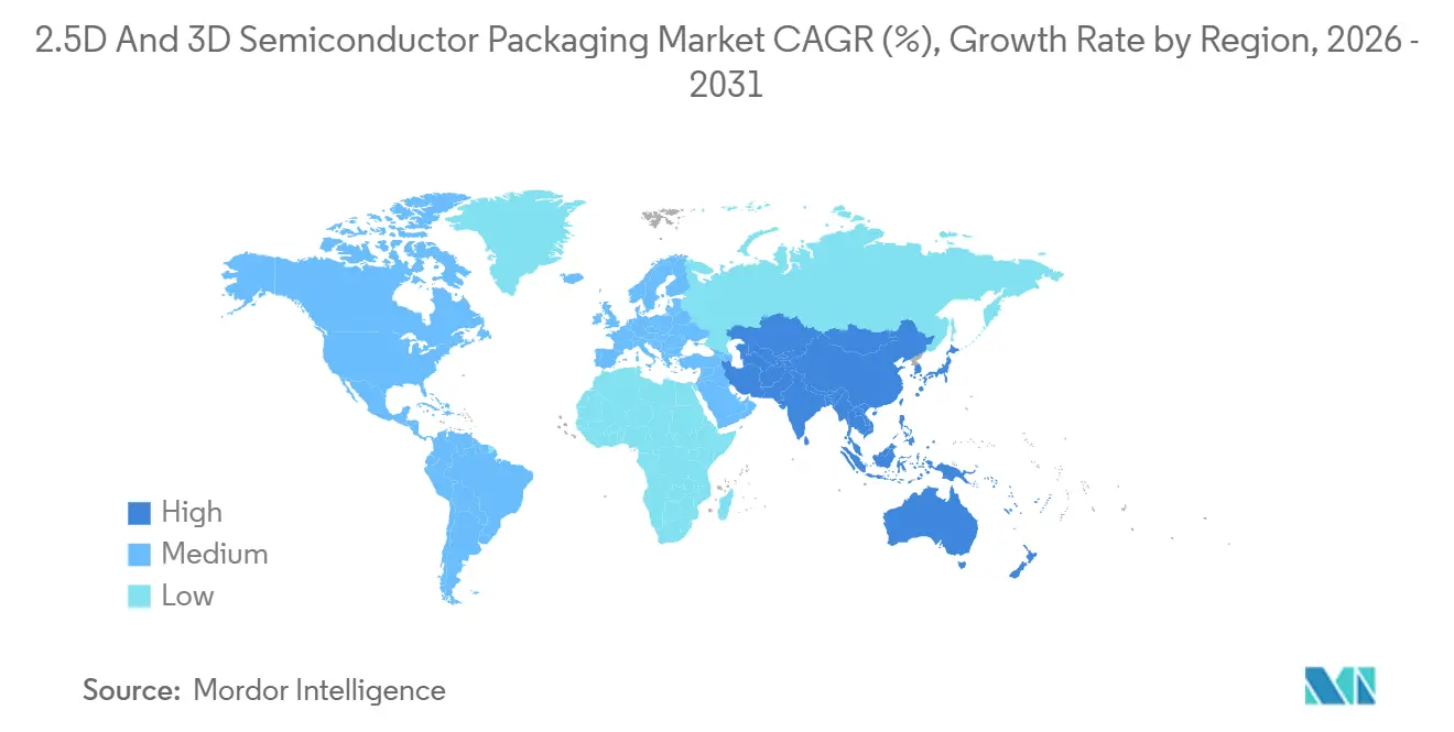
| Fastest Growing Market | Asia Pacific |
| Largest Market | Asia Pacific |
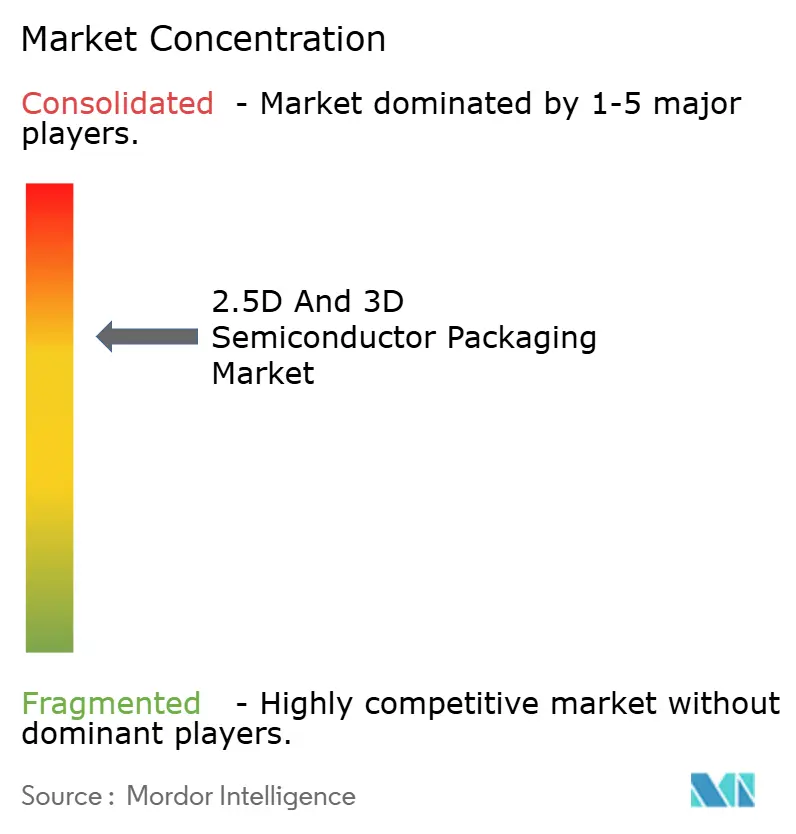
| Market Concentration | Medium |
Major Players *Disclaimer: Major Players sorted in no particular order Image © Mordor Intelligence. Reuse requires attribution under CC BY 4.0. | |
2.5D And 3D Semiconductor Packaging Market Analysis by Mordor Intelligence
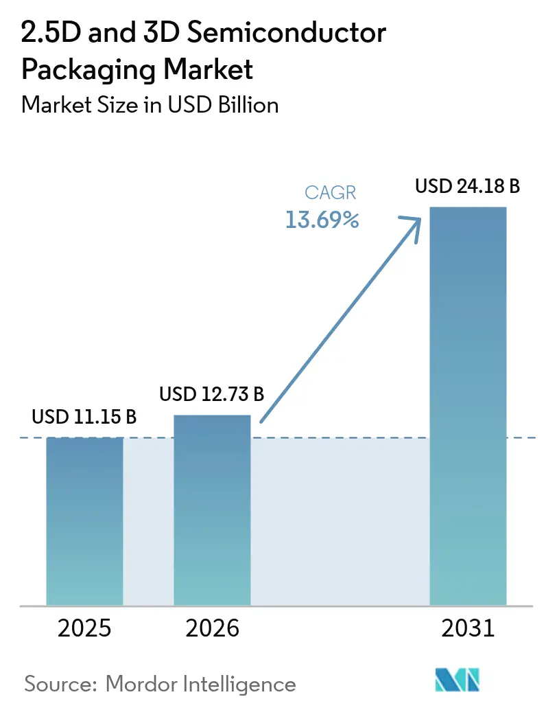
The 2.5D and 3D semiconductor packaging market size is expected to grow from USD 11.15 billion in 2025 to USD 12.73 billion in 2026 and is forecast to reach USD 24.18 billion by 2031 at 13.69% CAGR over 2026-2031. Heterogeneous integration is replacing monolithic scaling, and demand is rising for interposers, chiplets, and stacked high-bandwidth memory that keep compute and memory within millimeters of each other. Artificial-intelligence training clusters, electric-vehicle power modules, and co-packaged optics for data centers are lifting unit volumes across nearly every advanced-packaging flow. Despite high capital costs and persistent yield challenges, substrate suppliers, foundries, and outsourced assembly providers are accelerating tool installs to capture the widening performance-per-watt gap between advanced packaging and conventional printed-circuit-board design.
Key Report Takeaways
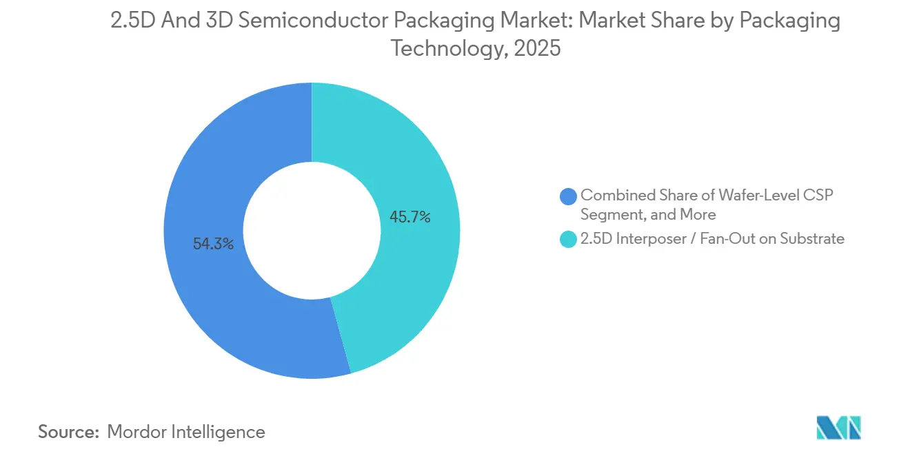
- By packaging technology, 2.5D interposer and fan-out on substrate solutions led with 45.72% of the 2.5D and 3D semiconductor packaging market share in 2025, while panel-level fan-out is advancing at a 13.83% CAGR to 2031.
- By application, memory captured 47.91% share of the 2.5D and 3D semiconductor packaging market size in 2025, and RF and photonics is projected to expand at 13.96% CAGR through 2031.
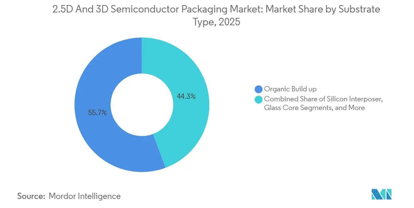
- By substrate type, organic build-up accounted for 55.74% of the 2.5D and 3D semiconductor packaging market size in 2025, whereas glass-core substrates are forecast to grow at 14.11% CAGR to 2031.
- By end-user industry, consumer electronics held 38.61% revenue share in 2025, and automotive and ADAS is the fastest-growing vertical at 14.34% CAGR to 2031.
- By geography, Asia-Pacific commanded 51.93% of the 2.5D and 3D semiconductor packaging market share in 2025, with a projected 14.41% CAGR during 2026-2031.
Note: Market size and forecast figures in this report are generated using Mordor Intelligence’s proprietary estimation framework, updated with the latest available data and insights as of 2026.
Global 2.5D And 3D Semiconductor Packaging Market Trends and Insights
Drivers Impact Analysis*
| Driver | (~) % Impact on CAGR Forecast | Geographic Relevance | Impact Timeline |
|---|---|---|---|
| AI/ML Workloads Demanding Ultra-High Memory Bandwidth | +3.8% | Global, concentrated in North America and Asia-Pacific data-center hubs | Medium term (2-4 years) |
| Rapid Uptake of Chiplet-Based Architectures | +2.9% | Global, with early adoption in North America and Taiwan foundries | Medium term (2-4 years) |
| Automotive ADAS Electrification Push | +2.4% | Europe, North America, and China automotive corridors | Long term (≥4 years) |
| Smartphone and Wearable Miniaturization | +1.9% | Asia-Pacific manufacturing hubs, global consumer markets | Short term (≤2 years) |
| Glass-Core Substrates Entering Volume Trials | +1.5% | Asia-Pacific and North America foundry ecosystems | Long term (≥4 years) |
| U.S. DoD Secure-Chip Mandates | +1.2% | United States and allied defense contractors | Medium term (2-4 years) |
| Source: Mordor Intelligence | |||


AI/ML Workloads Demanding Ultra-High Memory Bandwidth
Large-language-model training now requires terabytes of parameter updates per batch, so accelerator vendors are stacking eight or more high-bandwidth-memory dies on silicon interposers that sustain beyond-terabyte-per-second aggregate bandwidth. Orders for chip-on-wafer-on-substrate lines doubled during 2025, and lead times at leading foundries stretch well into 2027 as hyperscalers reserve capacity.[1]Taiwan Semiconductor Manufacturing Company, “TSMC Reports Fourth Quarter and Full Year 2025 Results,” investor.tsmc.com Flagship data-center GPUs introduced in late 2025 employ dual-reticle compute tiles linked on the same interposer, a topology competitors are replicating for next-generation inference devices. Mobile and edge inference engines, meanwhile, migrate toward lower-cost fan-out packages that embed LPDDR dies alongside neural processing units, keeping total accessible bandwidth high while keeping the bill of materials low.
Rapid Uptake of Chiplet-Based Architectures
Disaggregating dies into chiplets allows mixing mature I/O processes with cutting-edge compute nodes, improving yield and cutting mask cost. Mainstream client and server processors shipped since 2024 rely on four or more chiplets bonded on a 3D base die, and the open Universal Chiplet Interconnect Express standard finalized in 2024 assures multi-vendor interoperability.[2]Universal Chiplet Interconnect Express Consortium, “Standard Ratification,” uciexpress.org Automotive tier-one suppliers apply the same approach to merge radar, camera, and lidar compute into a single module that cuts board area 40%, easing over-the-air software updates.
Automotive ADAS Electrification Push
Electric-vehicle powertrains exceed 800 V, demanding silicon-carbide MOSFETs co-packaged with gate drivers and current sensors, configurations that grew 38% year-over-year in 2025. Advanced fan-out assemblies meet ISO 26262 ASIL-D functional-safety targets while shrinking module footprints. European Union's Euro 7 emissions standard, effective January 2026, mandates real-time particulate monitoring, spurring demand for sensor-fusion packages that combine MEMS accelerometers, pressure transducers, and microcontrollers in a single hermetic enclosures.
Smartphone and Wearable Miniaturization
Flagship smartphones released in 2025 integrated LPDDR5X memory and application processors within fan-out wafer-level packages less than 0.35 mm tall, lowering inductance 30% and extending battery life.[3]Apple Inc., “A18 Bionic Chip Technical Specifications,” apple.com Smartwatches now stack inertial sensors, Bluetooth radios, and OLED drivers in 3D packages occupying under 50 mm², enabling slimmer industrial designs. Wearable health monitors are embedding photoplethysmography sensors and analog front-ends in system-in-package assemblies that meet IP68 ingress-protection ratings, a requirement that drives adoption of molded underfill and hermetic lid-seal processes.
Restraints Impact Analysis*
| Restraint | (~) % Impact on CAGR Forecast | Geographic Relevance | Impact Timeline |
|---|---|---|---|
| Escalating CapEx for TSV and Interposer Fabs | -2.1% | Asia-Pacific and North America fab expansions | Short term (≤2 years) |
| Design-for-Test Complexity and Yield Loss | -1.6% | Global across all advanced-packaging nodes | Medium term (2-4 years) |
| Global Interposer Silicon-Ingot Shortage | -1.3% | Asia-Pacific supply chain, ripple effects worldwide | Short term (≤2 years) |
| Thermal-Management and Reliability Limits | -1.1% | High-performance computing and automotive segments | Long term (≥4 years) |
| Source: Mordor Intelligence | |||
Escalating CapEx for TSV and Interposer Fabs
A single 300 mm through-silicon-via line that processes 1,000 wafers per month demands investment exceeding USD 500 million, and equipment lead times increased to 18 months during 2025. Even projects subsidized by CHIPS Act funding will not reach volume until 2027, leaving smaller assembly players cash-constrained and fostering joint-venture structures that dilute returns. Smaller outsourced assembly and test providers lack the balance-sheet capacity to self-fund these expansions, forcing them to cede market share to integrated-device manufacturers with in-house packaging lines or to form joint ventures that dilute equity returns. Regulatory compliance with environmental permits for chemical waste and ultra-pure water discharge adds 12 to 18 months to fab construction timelines in Europe and North America, further inflating effective capital costs.
Design-for-Test Complexity and Yield Loss
Stacking multiple dies hides individual die boundaries and complicates fault isolation. The IEEE 1838 test-access standard reserves up to 8% of TSVs for probing, inflating area while still falling short of 95% coverage on ultra-wide buses. Automotive customers insist on near-zero defect rates, forcing the insertion of redundant tests that raise per-unit costs. Hybrid-bonds at 9 µm pitch delivered only 78% first-pass yield in early 2025 pilot lots, although machine-learning alignment algorithms lifted that figure to 85% by year-end.
*Our forecasts treat driver/restraint impacts as directional, not additive. The impact forecasts reflect baseline growth, mix effects, and variable interactions.
Segment Analysis
By Packaging Technology: Interposer Platforms Anchor Revenue While Panel Formats Promise Scale
2.5D interposer and fan-out on substrate flows accounted for 45.72% of the 2.5D and 3D semiconductor packaging market in 2025, reflecting entrenched use in data-center GPUs that demand terabyte-class bandwidth. Panel-level fan-out, processed on 600 mm square carriers, is forecast to post the fastest growth at 13.83% through 2031 as consortia validate new lithography aligners, molding presses, and handling tools. Yield improvements in molded redistribution layers and epoxy formulations with single-digit ppm thermal expansion help limit warpage across panels with wafers larger than 300 mm, while compliance with IEC 61340-5-1 electrostatic-discharge rules keeps contamination in check.
Panel-level fan-out provides 2.5 times the throughput per lithography step and reduces the cost per die, making advanced packaging viable for mid-tier smartphones and Internet-of-Things modules. Meanwhile, 3D-stacked through-silicon-via assemblies remain essential for high-bandwidth-memory cubes, even though capital intensity slows capacity additions. Wafer-level chip-scale packages retain dominance in value-driven mobile power-management ICs where thickness below 0.4 mm is critical. Together, these flows reinforce the structural expansion of the 2.5D and 3D semiconductor packaging market.


By Application: Memory Leads, RF and Photonics Gains Momentum
Memory captured 47.91% of the 2.5D and 3D semiconductor packaging market share in 2025, as each AI accelerator socket integrates up to 12 HBM cubes delivering over 3 TB/s sustained bandwidth. RF and photonics packaging, by contrast, is projected as the fastest-growing application at 13.96% CAGR to 2031, owing to co-packaged optics that eliminate separate pluggable modules and lower data-center power 20%. High-performance logic-server CPUs and AI GPUs-also leans on chiplet designs that exploit organic interposers for 2 TB/s die-to-die bandwidth.
Sensor-fusion packages in automotive ADAS merge analog front-ends with digital signal processors on fan-out redistribution layers, reducing electromagnetic interference. Power-management ICs continue migrating from discrete to wafer-level chip-scale form factors that halve footprint and shorten voltage-drop paths. These diverse workloads collectively underpin the multi-segment resilience of the 2.5D and 3D semiconductor packaging market.
By Substrate Type: Organic Build-Up Dominates, Glass Core Accelerates
Organic build-up substrates supplied 55.74% of demand in 2025 thanks to mature manufacturing and compatibility with surface-mount lines. Glass-core substrates are predicted to expand at 14.11% CAGR through 2031 after multiple foundries validated 10-layer redistribution with sub-2 µm lines, unlocking routing density for compute-memory-optical SoPs. Silicon interposers, though indispensable for leading-edge memory stacks, face raw-wafer shortages because prime ingots are prioritized for front-end logic fabs.
Advanced resin composites with ceramic fillers are growing in automotive modules that must survive 3,000 thermal cycles between -40 °C and 150 °C without delamination. Environmental regulations mandate halogen-free laminates, nudging materials cost slightly higher yet aligning with ISO 14001 sustainability objectives. Substrate innovation therefore remains a decisive lever in extending the 2.5D and 3D semiconductor packaging market size.
By End-User Industry: Consumer Electronics Largest, Automotive Fastest
Consumer electronics accounted for 38.61% of revenue in 2025, as smartphones, tablets, and wearables adopted wafer-level chip-scale and fan-out packages that achieve sub-0.35-mm profiles and enable IP68 sealing. Automotive and ADAS systems are forecast to grow the fastest, at a 14.34% CAGR over 2026-2031, as electric-vehicle platforms consolidate hundreds of power and sensor dies into multi-chip modules that reduce weight and simplify electromagnetic compliance. Data-center and HPC deployments continue to embed co-packaged optics, and telecom infrastructure integrates silicon-photonic transceivers into switch ASICs.
Industrial and IoT devices leverage system-in-package assemblies with 20-year field lifetimes, while defense and aerospace programs insist on trusted on-shore 3D assembly lines that comply with U.S. Department of Defense secure-chip mandates. Medical implants adopt titanium-lid hermetic packages that resist corrosion, underscoring the broadening vertical reach of the 2.5D and 3D semiconductor packaging industry.
Geography Analysis
Asia-Pacific generated 51.93% of 2025 revenue and is projected to advance at 14.41% CAGR through 2031 as Taiwan scales through-silicon-via capacity, South Korea moves hybrid-bonding into 9 µm pitch production, and China accelerates localization of organic substrates under “Made in China 2025.” Government subsidies, existing substrate supply chains, and proximity to consumer-electronics OEMs reinforce regional leadership.
North America ranked second with expanding capacity at Intel’s Arizona and New Mexico Foveros facilities and Amkor’s CHIPS-funded Arizona plant, both targeting 2027 volume. Federal procurement rules favor domestic content, redirecting capital that might otherwise flow offshore. Defense contractors also prefer on-shore trusted foundries for classified workloads, further lifting regional demand.
Europe, supported by the European Chips Act and EUR 3.3 billion (USD 3.5 billion) in incentives, is piloting organic and glass-core substrate lines in Germany, France, and Spain. South America attracts automotive tier-one suppliers building localized EV module assembly, while the Middle East deploys AI-capable data centers and Africa pilots smart-grid IoT nodes. Collectively, these initiatives widen the global footprint of the 2.5D and 3D semiconductor packaging market.

Competitive Landscape
The 2.5D and 3D semiconductor packaging market shows moderate concentration, the top five players-TSMC, Samsung, Intel, ASE Technology, and Amkor-controlled a considerable share of 2025 revenue, but no single firm exceeded 20%. Integrated-device manufacturers expand internal lines for strategic control, while outsourced assembly and test companies invest billions in TSV and hybrid-bond tooling to keep pace with complex multi-die programs. Strategic moves include foundries acquiring substrate makers to lock in supply and equipment consortia pooling capital to industrialize panel-level fan-out.
Open standards, notably Universal Chiplet Interconnect Express, reduce vendor lock-in and encourage multi-sourcing, which diffuses share and fosters collaboration among nominal rivals. Start-ups specializing in glass-core substrates and RF-photonics integration provide niche disruption, securing early design wins in co-packaged optics for 1.6 Tbps Ethernet switches that cut data-center power 22%.
Machine-learning-driven yield analytics shorten hybrid-bond alignment cycles from 48 hours to 24 hours, demonstrating that software expertise is an emerging differentiator even within traditional manufacturing domains. Compliance with IEEE 1838 and IEC contamination standards further levels the playing field, ensuring newcomers meet system-maker qualification without multi-year in-house development.
2.5D And 3D Semiconductor Packaging Industry Leaders
Amkor Technology Inc.
Intel Corporation
Samsung Electronics Co. Ltd
ASE Technology Holding Co., Ltd.
Taiwan Semiconductor Manufacturing Company Limited
- *Disclaimer: Major Players sorted in no particular order

Recent Industry Developments
- February 2026: TSMC committed USD 3.5 billion to expand chip-on-wafer-on-substrate capacity in Taiwan, targeting 50,000 wafer starts per month by Q4 2027.
- January 2026: Samsung Electronics entered volume production of fourth-generation 9 µm hybrid-bonding in Pyeongtaek to support 2027 flagship smartphone processors.
- December 2025: Intel finished constructing its Foveros 3D packaging plant in New Mexico, backed by USD 600 million in CHIPS Act funding, with first shipments set for Q2 2026.
- November 2025: ASE Technology and Qualcomm formed a panel-level fan-out joint development program, planning 10,000 panels per month pilot output by mid-2027.
- October 2025: Amkor Technology’s USD 2 billion Arizona advanced-packaging facility received final environmental permits, enabling equipment installs for 2027 ramp-up.


Global 2.5D And 3D Semiconductor Packaging Market Report Scope
2.5D/3D is a packaging methodology for having multiple ICs inside the package. In a 2.5D structure, two or more active semiconductor chips are positioned side-by-side on a silicon interposer to reach extremely high die-to-die interconnect density. In a 3D structure, active chips are combined by die stacking for the shortest interconnect and smallest package footprint. In recent years, 2.5D and 3D have gained momentum as ideal chipset integration platforms due to their merits in achieving extremely high packaging density and energy efficiency.
The 2.5D and 3D Semiconductor Packaging Market Report is Segmented by Packaging Technology (2.5D Interposer/Fan-Out on Substrate, 3D Stacked TSV/Hybrid Bond, Wafer-Level CSP, and Panel-Level Fan-Out), Application (High-Performance Logic, Memory HBM and 3D NAND, RF and Photonics, Mixed-Signal and Sensor Integration, and Power Management ICs), Substrate Type (Organic Build-Up, Silicon Interposer, Glass Core, and Advanced Resin Composite), End-User Industry (Consumer Electronics, Data Center and HPC, Communications and Telecom, Automotive and ADAS, Industrial and IoT, Defense and Aerospace, and Medical Devices), and Geography (North America, South America, Europe, Asia-Pacific, Middle East, and Africa). The Market Forecasts are Provided in Terms of Value USD.
| 2.5D Interposer / Fan-Out on Substrate |
| 3D Stacked (TSV / Hybrid Bond) |
| Wafer-Level CSP |
| Panel-Level Fan-Out |
| High-Performance Logic |
| Memory (HBM, 3D NAND) |
| RF and Photonics |
| Mixed-Signal and Sensor Integration |
| Power Management ICs |
| Organic Build-Up |
| Silicon Interposer |
| Glass Core |
| Advanced Resin Composite |
| Consumer Electronics |
| Data Center and HPC |
| Communications and telecom |
| Automotive and ADAS |
| Industrial and IoT |
| Defense and Aerospace |
| Medical Devices |
| Rest of End-User Industries |
| North America | United States |
| Canada | |
| Mexico | |
| South America | Brazil |
| Argentina | |
| Rest of South America | |
| Europe | Germany |
| United Kingdom | |
| France | |
| Spain | |
| Rest of Europe | |
| Asia-Pacific | China |
| India | |
| Japan | |
| South Korea | |
| ASEAN | |
| Rest of Asia-Pacific | |
| Middle East | Saudi Arabia |
| United Arab Emirates | |
| Turkey | |
| Rest of Middle East | |
| Africa | South Africa |
| Nigeria | |
| Rest of Africa |
| By Packaging Technology | 2.5D Interposer / Fan-Out on Substrate | |
| 3D Stacked (TSV / Hybrid Bond) | ||
| Wafer-Level CSP | ||
| Panel-Level Fan-Out | ||
| By Application | High-Performance Logic | |
| Memory (HBM, 3D NAND) | ||
| RF and Photonics | ||
| Mixed-Signal and Sensor Integration | ||
| Power Management ICs | ||
| By Substrate Type | Organic Build-Up | |
| Silicon Interposer | ||
| Glass Core | ||
| Advanced Resin Composite | ||
| By End-User Industry | Consumer Electronics | |
| Data Center and HPC | ||
| Communications and telecom | ||
| Automotive and ADAS | ||
| Industrial and IoT | ||
| Defense and Aerospace | ||
| Medical Devices | ||
| Rest of End-User Industries | ||
| By Geography | North America | United States |
| Canada | ||
| Mexico | ||
| South America | Brazil | |
| Argentina | ||
| Rest of South America | ||
| Europe | Germany | |
| United Kingdom | ||
| France | ||
| Spain | ||
| Rest of Europe | ||
| Asia-Pacific | China | |
| India | ||
| Japan | ||
| South Korea | ||
| ASEAN | ||
| Rest of Asia-Pacific | ||
| Middle East | Saudi Arabia | |
| United Arab Emirates | ||
| Turkey | ||
| Rest of Middle East | ||
| Africa | South Africa | |
| Nigeria | ||
| Rest of Africa | ||


Key Questions Answered in the Report
What revenue will 2.5D and 3D semiconductor packaging generate by 2031?
The market is forecast to reach USD 24.18 billion by 2031, expanding at 13.69% CAGR over 2026-2031.
Which application currently dominates advanced packaging demand?
High-bandwidth-memory modules for AI training systems held 47.91% of 2025 revenue.
Why are panel-level fan-out packages gaining attention?
Processing on 600 mm square panels boosts lithography throughput 2.5-fold and lowers die cost, driving a 13.83% CAGR forecast through 2031.
Which end-user vertical is growing the fastest?
Automotive and ADAS solutions are projected to advance at 14.34% CAGR thanks to electric-vehicle electrification and sensor-fusion modules.
How concentrated is the supplier landscape?
The five largest vendors captured about 60% of 2025 revenue, indicating moderate concentration without a single dominant leader.
What region leads production and why?
Asia-Pacific commands 51.93% of revenue due to extensive substrate supply chains, foundry capacity, and consumer-electronics proximity.
Page last updated on:


