Non-Volatile Memory Market Size and Share
Market Overview
| Study Period | 2020 - 2031 |
|---|---|
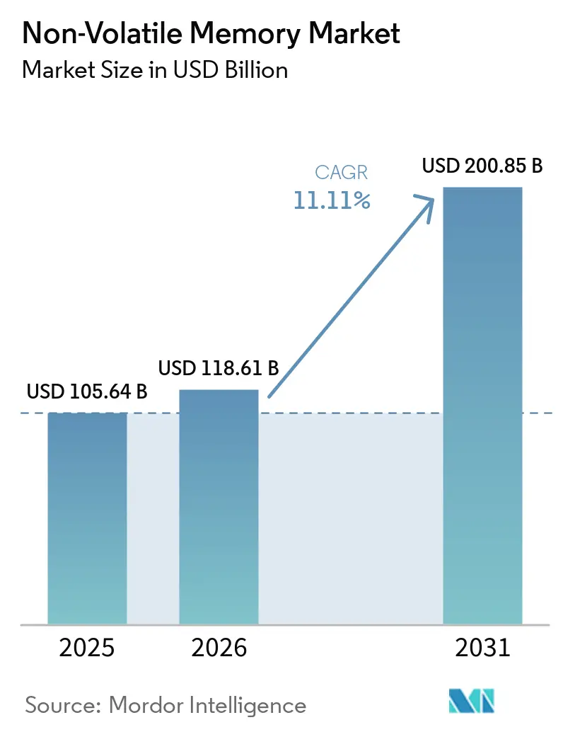
| Market Size (2026) | USD 118.61 Billion |
| Market Size (2031) | USD 200.85 Billion |
| Growth Rate (2026 - 2031) | 11.11% CAGR |
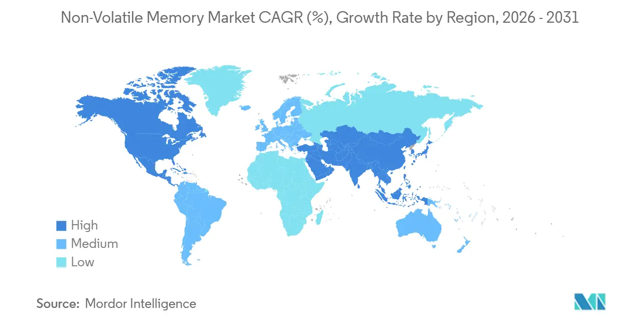
| Fastest Growing Market | Middle East |
| Largest Market | Asia Pacific |
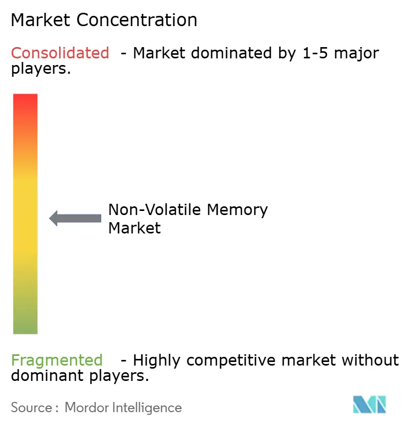
| Market Concentration | Medium |
Major Players *Disclaimer: Major Players sorted in no particular order Image © Mordor Intelligence. Reuse requires attribution under CC BY 4.0. | |
Non-Volatile Memory Market Analysis by Mordor Intelligence
The non-volatile memory market size is projected to expand from USD 105.64 billion in 2025 and USD 118.61 billion in 2026 to USD 200.85 billion by 2031, registering a CAGR of 11.11% between 2026 and 2031. Enterprises are redesigning storage hierarchies so that hyperscalers push key-value caches onto persistent media, while automotive original equipment manufacturers embed terabyte-class solid-state drives in software-defined vehicles. Interface upgrades to PCIe Gen 6 and NVMe-over-Fabrics reduce protocol overhead and unlock the bandwidth required for generative artificial intelligence, tightening the supply of high-performance NAND. Simultaneously, magnetoresistive random-access memory (MRAM) and resistive random-access memory (ReRAM) are gaining traction in edge gateways that require unlimited write endurance. Government incentives in the United States, Japan, and South Korea, combined with export-control uncertainty, steer capital expenditures toward domestic fabs capable of delivering advanced nodes at scale.
Key Report Takeaways
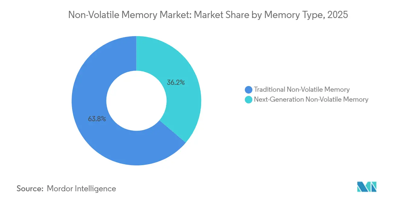
- By memory type, flash memory led with 63.78% of the non-volatile memory market share in 2025, while MRAM is forecast to grow at an 11.97% CAGR through 2031.
- By end-user industry, consumer electronics accounted for 44.81% of demand in 2025, whereas automotive electronics is projected to expand at a 11.56% CAGR through 2031.
- By interface, PCIe/NVMe captured 53.29% of the non-volatile memory market in 2025 and is advancing at a 11.84% CAGR through 2031.
- By density, modules ≥8 Gb accounted for 37.53% of the non-volatile memory market in 2025 and are slated to grow at a 12.06% CAGR over 2026-2031.
- By application, enterprise storage accounted for 41.39% of shipments in 2025, while connected and wearable devices posted the highest projected CAGR of 12.11% during the forecast period.
- By geography, Asia-Pacific led with 46.11% revenue share in 2025, whereas the Middle East is expected to record a 12.25% CAGR through 2031.
Note: Market size and forecast figures in this report are generated using Mordor Intelligence’s proprietary estimation framework, updated with the latest available data and insights as of January 2026.
Global Non-Volatile Memory Market Trends and Insights
Drivers Impact Analysis*
| Driver | (~) % Impact on CAGR Forcast | Geographic Relevance | Impact Timeline |
|---|---|---|---|
| Exploding Data-Center Build-Outs Elevate Demand for Enterprise-Class NVM | +2.8% | Global, concentrated in North America and Asia-Pacific hyperscale regions | Medium term (2-4 years) |
| Proliferation of Automotive ADAS and In-Vehicle Infotainment | +2.1% | Global, led by Europe and Asia-Pacific automotive hubs | Long term (≥ 4 years) |
| Edge AI Workloads Requiring Persistent, Low-Latency Storage | +1.9% | North America and Asia-Pacific edge deployments, spillover to Europe | Medium term (2-4 years) |
| Mainstream Adoption of UFS 4.0 Interface in Smartphones | +1.6% | Asia-Pacific manufacturing base, global smartphone markets | Short term (≤ 2 years) |
| Commercialization of 3D-XPoint-Based Persistent Memory Modules | +0.9% | North America and Europe enterprise segments | Long term (≥ 4 years) |
| Government Incentives for Domestic Semiconductor Manufacturing | +1.4% | United States, Japan, South Korea, and European Union member states | Long term (≥ 4 years) |
| Source: Mordor Intelligence | |||


Exploding Data-Center Build-Outs Elevate Demand for Enterprise-Class NVM
Hyperscalers plan to deploy 100 GW of new data-center capacity between 2026 and 2030, and each rack integrates petabyte-scale all-flash arrays to serve inference workloads. PCIe Gen 6 solid-state drives, such as Micron’s 9650, deliver 28 GB/s of sequential read throughput, closing the gap between compute and storage throughput.[1]Micron Technology, “Micron 9650 PCIe Gen 6 SSD Datasheet,” micron.com NVIDIA’s Inference Compute Memory Storage Platform offloads key-value stores from high-bandwidth memory to enterprise SSDs, trimming accelerator costs by 30% while holding retrieval latency below one millisecond. This shift favors triple-level cell NAND that withstands 3 drive writes per day, elevating the non-volatile memory market as a strategic buffer between DRAM and object storage. As server refresh cycles accelerate from five to three years, suppliers that master firmware-level endurance optimization secure long-term contracts with hyperscalers.
Proliferation of Automotive ADAS and In-Vehicle Infotainment
Software-defined vehicles allocate 2-4 TB of storage for high-definition maps, over-the-air updates, and sensor-fusion logs. Infineon’s SEMPER NOR Flash earned ASIL-D safety certification under ISO 26262, enabling fail-operational boot architectures in Level 3 autonomy. Universal Flash Storage 4.0 replaces legacy embedded MultiMediaCard to sustain 4K video streaming at lower power.[2]JEDEC Solid State Technology Association, “UFS 4.0 Standard JESD220E,” jedec.org Automotive-grade NAND must survive -40 °C to 125 °C and 3 000 program-erase cycles, commanding a 40% premium over consumer-grade modules. The transition from 12-V to 48-V electrical systems introduces voltage transients, prompting original equipment manufacturers to specify on-die error-correcting code and power-loss protection, boosting the bill of materials yet ensuring data integrity during regenerative braking.
Edge AI Workloads Requiring Persistent, Low-Latency Storage
Retail point-of-sale terminals, industrial vision systems, and smart-city gateways embed MRAM to preserve model weights during power cycling while delivering sub-10 µs read latency. Everspin’s UNISYST MRAM combines non-volatility with unlimited write endurance, removing wear-leveling overhead in log-heavy applications. Weebit Nano licensed its ReRAM intellectual property to Texas Instruments, enabling foundries to integrate embedded non-volatile memory at 28 nm nodes. IEEE studies in 2025 show that non-volatile SRAM cuts standby power by 1 000× compared to flash in wearables, extending battery life from days to weeks. IEEEXPLORE.IEEE.ORG. These developments widen the non-volatile memory market for densities below 1 Gb where flash’s millisecond-class latency fails to meet real-time edge requirements.
Mainstream Adoption of UFS 4.0 Interface in Smartphones
JEDEC introduced Universal Flash Storage 4.0 in 2024, doubling lane bandwidth to 4.8 GB/s and adding host-performance booster extensions. Google’s Pixel 10 and Samsung’s Galaxy S26, launched in 2026, shipped with 512 GB and 1 TB UFS 4.0 modules, enabling on-device generative AI without cloud connectivity. Kioxia began sampling UFS 5.0 in February 2026 with 9.6 GB/s throughput, laying the groundwork for 2027 flagships. As mid-tier vendors migrate from embedded MultiMediaCard 5.1 to UFS 3.1, legacy interfaces contract by 15% annually, reallocating wafer output to higher-margin UFS packages. Rapid interface adoption sustains bit growth, reinforcing the non-volatile memory market's trajectory in mobile devices.
Restraints Impact Analysis*
| Restraint | (~) % Impact on CAGR Forecast | Geographic Relevane | Impact Timeline |
|---|---|---|---|
| Low Write-Endurance in Certain NVM Architectures | -1.2% | Global, particularly the enterprise and data-center segments | Medium term (2-4 years) |
| Thermal Runaway Risks in High-Density 3D NAND Stacks | -0.9% | Global, acute in high-performance computing and enterprise storage | Short term (≤ 2 years) |
| Geopolitical Export Controls on Advanced Memory Nodes | -0.7% | Asia-Pacific manufacturing, North America and Europe end markets | Long term (≥ 4 years) |
| Supply-Demand Cyclicality Causing Price Volatility | -0.8% | Global, pronounced in consumer electronics and enterprise procurement | Short term (≤ 2 years) |
| Source: Mordor Intelligence | |||
Low Write-Endurance in Certain NVM Architectures
Quad-level cell NAND endures only 500 program-erase cycles and penta-level cell just 200, compared with 3 000 for triple-level cell. Database logging and AI checkpointing reach write amplification factors above 5, exhausting quad-level cell drives within 18 months. Machine-learning controllers extend life by 40% but add 28% over-provisioning, eroding cost advantages. Hyperscalers now reserve triple-level cells for hot data and relegate quad-level cells to cold storage, fragmenting procurement plans. The endurance gap opens white space for MRAM and ReRAM in industrial loggers and automotive black boxes, where replacement costs exceed initial module pricing.
Thermal Runaway Risks in High-Density 3D NAND Stacks
Layer counts beyond 300 elevate junction temperatures to 85 °C under sustained writes, triggering thermal runaway as adjacent cells leak charge through heated oxides. Kioxia’s 245.76 TB LC9 drives require liquid cooling that adds USD 150 per unit and complicates rack integration. JEDEC’s JESD218 instructs throttling at 80 °C, but throughput drops 60% when throttled. Samsung and SK Hynix are testing silicon-germanium channels with lower leakage, yet five-nanometer migrations push volume production to 2028. Until then, thermal constraints slow the qualification of ultra-dense NAND in high-performance computing clusters.
*Our forecasts treat driver/restraint impacts as directional, not additive. The impact forecasts reflect baseline growth, mix effects, and variable interactions.
Segment Analysis
By Memory Type: Non-Volatile Memory-MRAM Disrupts Flash Hegemony
Flash memory accounted for 63.78% of the non-volatile memory market share in 2025. Steady cost declines sustained its dominance, yet MRAM is projected to grow at an 11.97% CAGR through 2031. The non-volatile memory market size tied to flash continues to expand, although write-heavy edge workloads expose endurance bottlenecks. MRAM shipments of 64 Mb, 128 Mb, and 256 Mb entered industrial controllers, railway signaling, and aviation black boxes, replacing NOR Flash where firmware updates exceed NAND’s block-erase limitations.
Second-generation spin-orbit torque technology raises MRAM densities toward 1 Gb, and integration on 28 nm embedded logic yields deterministic 10 ns writes. Ferroelectric RAM services RFID tags that need 10^14 cycles but only kilobyte capacities. ReRAM and 3D XPoint aim for the storage-class memory tier, yet Intel’s Optane exit created a commercialization pause that startups like Weebit Nano now aim to overcome through foundry alliances. These dynamics illustrate a pivot where system architects pair high-capacity NAND with byte-addressable MRAM to balance endurance and cost, a design that reshapes the non-volatile memory market over the forecast horizon.

By End-User Industry: Automotive Electronics Accelerates Past Consumer
Consumer electronics accounted for 44.81% of demand in 2025, driven by more than 2 billion smartphones, tablets, and laptops. Automotive electronics, however, is anticipated to post an 11.56% CAGR through 2031 as electric vehicle volumes rise and advanced driver-assistance systems require ASIL-D-certified storage. The non-volatile memory market size attributable to vehicles multiplies as each software-defined platform embeds 10-20 electronic control units with 256 MB to 4 GB flash.
High-definition maps, over-the-air updates, and sensor logs are cached locally, elevating per-vehicle non-volatile memory content eightfold relative to internal-combustion models. Telecommunications infrastructure accounts for 28% of enterprise SSD shipments, while healthcare archiving mandates AES-256-encrypted NAND with 10-year retention. Industrial automation specifies shock-resistant NAND rated to -40 °C, and retail terminals adopt UFS 3.1 to cut boot times. Diversified end users reduce cyclicality, insulating suppliers when smartphone refresh cycles extend beyond three years.
By Interface: PCIe/NVMe Dominance Extends Through Gen 6
PCIe/NVMe accounted for 53.29% of 2025 shipments and is projected to grow at an 11.84% CAGR during the forecast period. This growth is driven by the increasing adoption of PCIe Gen 6 x4 links, which deliver sustained read speeds of 28 GB/s and write speeds of 14 GB/s. These advancements enable AI clusters to seamlessly synchronize gradients across 10,000 GPUs, eliminating I/O stalls and improving overall efficiency. Additionally, NVMe-over-Fabrics technology is transforming storage infrastructure by disaggregating storage resources. This innovation enables the creation of petabyte-scale elastic storage pools with sub-100 µs latency, catering to the growing demand for high-performance, scalable storage in data-intensive applications.
SATA dwindles as motherboard designs drop the interface to cut costs and free space. USB4 portable drives cater to 8K video creators yet throttle under sustained workloads due to thermal budgets in compact enclosures. Serial peripheral interface and I ²C dominate firmware storage on microcontrollers and sensors, where pin count and milliwatt power trump throughput. As PCIe’s coherent attachment blurs the boundaries between DRAM and storage, the non-volatile memory market is shifting toward composable infrastructure that provisions capacity on demand.
By Density: High-Capacity Modules Propel ≥8 Gb Segment
Modules ≥8 Gb held 37.53% share in 2025 and are projected to grow at a 12.06% CAGR during the forecast period. High-end smartphone flagships now ship with storage capacities ranging from 512 GB to 1 TB, utilizing UFS 4.0 technology, while enterprise SSDs have scaled up to 245.76 TB per E3.S drive. The adoption of three-dimensional NAND technology with 218 layers has enabled the production of 2 Tb dies. This advancement has significantly reduced the cost per bit, making NAND-based storage solutions more cost-effective and allowing them to finally undercut hard disk drives in cold storage applications.
Mid-tier densities, ranging from 2 GB to 4 GB, strike a balance between cost efficiency and endurance, making them suitable for human-machine interfaces in industrial settings and automotive applications. Meanwhile, sub-256-MB NOR Flash continues to serve niche applications, such as BIOS and configuration storage. Growth in the memory market is primarily concentrated in terabyte-class tiers, as hyperscalers and smartphone manufacturers absorb the majority of incremental wafer output. In contrast, mid-density segments are now primarily competing on price, leading to a clear market bifurcation. This shift is reshaping fabrication strategies, compelling suppliers to allocate new production lines to ultra-dense quad-level cell technologies while simultaneously extending the lifecycle of mature nodes to cater to legacy parts.


By Application: Connected Devices Outpace Enterprise Storage
Enterprise storage accounted for 41.39% of 2025 shipments, but connected and wearable devices are forecast to expand at a 12.11% CAGR. Non-volatile SRAM significantly reduces standby power consumption by up to 1,000 times in smartwatches, enabling continuous electrocardiogram logging without daily charging.[3]IEEE Xplore Digital Library, “Ultra-Low-Power NVS-RAM for Wearable ECG Devices,” ieeexplore.ieee.org AI-enabled wearables are increasingly adopting 64 GB UFS packages, driven by the integration of local caching for large language models.
In the industrial automation sector, MRAM is gaining traction for its ability to perform deterministic writes within 100 microseconds, a critical requirement for synchronizing multi-axis motion control systems. In the automotive industry, advanced driver-assistance systems (ADAS) are leveraging a combination of NOR Flash boot partitions and high-endurance NAND data logs to comply with ISO 26262 functional safety standards and UNECE R155 cybersecurity regulations. As billions of sensors continue to connect to the Internet of Things (IoT), the demand for low-power, shock-resistant storage solutions is driving the expansion of the non-volatile memory market beyond its traditional applications in servers and personal computers.
Geography Analysis
Asia-Pacific accounted for 46.11% of non-volatile memory revenue in 2025, led by Samsung, SK hynix, Kioxia, and Taiwanese foundries, which supply 75% of global NAND output. Regional growth is projected at an 11.84% CAGR as South Korea’s 21.6 trillion won (USD 15.7 billion) tax credits finance the Yongin cluster, and Japan’s Ministry of Economy, Trade and Industry grants JPY 500 billion (USD 3.4 billion) to Micron’s Hiroshima fab. China accelerates domestic NAND at Yangtze Memory, but U.S. export controls on extreme-ultraviolet scanners stall progress beyond 128-layer nodes.
North America held 24% share in 2025, buoyed by Amazon, Microsoft, and Google, whose collective 40 EB of enterprise SSD deployments anchor long-term procurement. The CHIPS and Science Act unlocks USD 52.7 billion in subsidies, with USD 6.44 billion for Micron’s New York and Idaho expansions, USD 4.745 billion for Samsung’s Texas line, and USD 950 million for SK hynix packaging in Indiana.[4]U.S. Department of Commerce, “CHIPS and Science Act Funding Awards,” commerce.gov Europe captured 16% demand as Germany’s automotive tier-ones source ASIL-D NAND from Infineon and STMicroelectronics.
The Middle East posts the fastest regional CAGR of 12.25%, driven by USD 33.79 billion in sovereign-wealth spending on data-center infrastructure for smart-city and artificial intelligence services. South America and Africa together account for 8% of the market and rely on edge caching to offset limited backbone bandwidth, using UFS packages in base-station servers. Government subsidies reduce geographic concentration, yet the non-volatile memory market still hinges on three Northeast Asian economies, leaving supply vulnerable to seismic, political, and export-control events.

Competitive Landscape
The non-volatile memory market remains moderately consolidated. Samsung, SK hynix, Micron, Kioxia, and Western Digital together captured 82% of 2025 NAND and DRAM revenue, reflecting USD 15 billion-plus fab investments that deter new entrants. Samsung tripled high-bandwidth memory output in early 2026 and secured a multiyear supply with Nvidia and AMD, locking in 60% of 2026 high-bandwidth memory shipments. SK hynix mass produces 1c-nanometer DRAM that feeds high-bandwidth memory 4 stacks, while Micron leads PCIe Gen 6 SSDs with 232-layer NAND.
Vertical integration extends from wafers to firmware; Samsung designs controllers that slash garbage-collection overhead, and SK hynix co-optimizes firmware and DRAM buffers for AI caches. Kioxia and Western Digital operate the Kitakami Fab2, subsidized by JPY 774.5 billion (USD 5.3 billion) from Japan to secure automotive supply. Start-ups such as Everspin, Weebit Nano, and Crossbar focus on licensing MRAM and ReRAM intellectual property to foundries like TSMC, sidestepping USD 20 billion fab outlays yet depending on ecosystem adoption.
Technology roadmaps converge on composable infrastructure; Dell’s PowerFlex and Nvidia’s Magnum-IO bypass storage-area networks with NVMe-over-Fabrics failover below 100 µs. Suppliers respond by acquiring software-defined storage start-ups to bundle hardware and orchestration, protecting gross margins against commoditization. Automotive and industrial verticals reward vendors that certify to ISO 26262, IEC 62304, and NIST firmware resilience, creating niche barriers that offset the scale advantage of the storage oligopoly.
Non-Volatile Memory Industry Leaders
Samsung Electronics Co. Ltd
Micron Technology Inc.
SK Hynix Inc.
Kioxia Holdings Corp.
Solidigm Inc.
- *Disclaimer: Major Players sorted in no particular order

Recent Industry Developments
- March 2026: Samsung Electronics and AMD signed an agreement to supply high-bandwidth memory 4 for MI400 accelerators, with first deliveries slated for Q4 2026.
- February 2026: Micron Technology started volume production of 9650 PCIe Gen 6 enterprise SSDs rated at 28 GB/s sequential read and 3 M IOPS random read.
- February 2026: Samsung Electronics ramped high-bandwidth memory 4 to 1.5 TB/s per stack and 36 GB capacity via 12-high stacking.
- February 2026: JEDEC released Universal Flash Storage 5.0 doubling bandwidth to 9.6 GB/s; Kioxia began sampling devices for 2027 smartphones.


Global Non-Volatile Memory Market Report Scope
The non-volatile memory market refers to the global industry focused on the development, manufacturing, and commercialization of memory technologies that retain stored data even when power is removed. Unlike volatile memory, NVM solutions provide persistent storage, making them essential for a wide range of electronic devices and systems that require reliable, long-term data retention and fast access.
The Non-Volatile Memory Report is Segmented by Memory Type (Traditional Non-Volatile Memory, and Next-Generation Non-Volatile Memory), End-User Industry (Consumer Electronics, Retail, IT and Telecom, Healthcare, and More), Interface (PCIe/NVMe, SATA, USB, SPI/I²C, and More), Density (≤256 Mb, 512 Mb–1 Gb, 2 Gb–4 Gb, and ≥8 Gb), Application (Enterprise Storage, Connected and Wearable Devices, Industrial Automation, Automotive Electronics, and More), and Geography (North America, South America, Europe, Asia-Pacific, Middle East, and Africa). The Market Forecasts are Provided in Terms of Value (USD).
| Traditional Non-Volatile Memory | Flash Memory |
| EEPROM | |
| SRAM | |
| EPROM | |
| Rest of Traditional Non-Volatile Memory | |
| Next-Generation Non-Volatile Memory | MRAM |
| FRAM | |
| ReRAM | |
| 3D XPoint | |
| Nano RAM | |
| Rest of Next-Generation Non-Volatile Memory |
| Consumer Electronics |
| Retail |
| IT and Telecom |
| Healthcare |
| Other End-User Industries |
| PCIe/NVMe |
| SATA |
| USB |
| SPI/I²C |
| Other Interfaces |
| ≤256 Mb |
| 512 Mb–1 Gb |
| 2 Gb–4 Gb |
| ≥8 Gb |
| Enterprise Storage |
| Connected and Wearable Devices |
| Industrial Automation |
| Automotive Electronics |
| Rest of Applications |
| North America | United States |
| Canada | |
| Rest of North America | |
| South America | Brazil |
| Argentina | |
| Rest of South America | |
| Europe | United Kingdom |
| Germany | |
| France | |
| Russia | |
| Rest of Europe | |
| Asia-Pacific | China |
| Japan | |
| South Korea | |
| India | |
| Rest of Asia-Pacific | |
| Middle East | Saudi Arabia |
| United Arab Emirates | |
| Turkey | |
| Rest of Middle East | |
| Africa | South Africa |
| Nigeria | |
| Rest of Africa |
| By Memory Type | Traditional Non-Volatile Memory | Flash Memory |
| EEPROM | ||
| SRAM | ||
| EPROM | ||
| Rest of Traditional Non-Volatile Memory | ||
| Next-Generation Non-Volatile Memory | MRAM | |
| FRAM | ||
| ReRAM | ||
| 3D XPoint | ||
| Nano RAM | ||
| Rest of Next-Generation Non-Volatile Memory | ||
| By End-User Industry | Consumer Electronics | |
| Retail | ||
| IT and Telecom | ||
| Healthcare | ||
| Other End-User Industries | ||
| By Interface | PCIe/NVMe | |
| SATA | ||
| USB | ||
| SPI/I²C | ||
| Other Interfaces | ||
| By Density | ≤256 Mb | |
| 512 Mb–1 Gb | ||
| 2 Gb–4 Gb | ||
| ≥8 Gb | ||
| By Application | Enterprise Storage | |
| Connected and Wearable Devices | ||
| Industrial Automation | ||
| Automotive Electronics | ||
| Rest of Applications | ||
| By Geography | North America | United States |
| Canada | ||
| Rest of North America | ||
| South America | Brazil | |
| Argentina | ||
| Rest of South America | ||
| Europe | United Kingdom | |
| Germany | ||
| France | ||
| Russia | ||
| Rest of Europe | ||
| Asia-Pacific | China | |
| Japan | ||
| South Korea | ||
| India | ||
| Rest of Asia-Pacific | ||
| Middle East | Saudi Arabia | |
| United Arab Emirates | ||
| Turkey | ||
| Rest of Middle East | ||
| Africa | South Africa | |
| Nigeria | ||
| Rest of Africa | ||


Key Questions Answered in the Report
What is the projected value of the non-volatile memory market in 2031?
The market is forecast to reach USD 200.85 billion by 2031, reflecting an 11.11% CAGR during 2026-2031.
Which segment is expected to grow fastest within non-volatile storage?
MRAM is projected to post an 11.97% CAGR through 2031, driven by edge AI and automotive safety uses.
How do government incentives affect semiconductor capacity?
Subsidies under the U.S. CHIPS Act and Japan's resilience program lower capital costs for new fabs, encouraging domestic production and diversifying supply sources.
Why are PCIe/NVMe interfaces overtaking SATA?
PCIe Gen 6 SSDs deliver 28 GB/s sequential read, cutting latency by 40% versus SATA and supporting disaggregated NVMe-over-Fabrics storage.
What challenge limits adoption of ultra-dense 3D NAND?
Thermal runaway above 300 layers forces liquid cooling and throttling, reducing performance and delaying deployment in high-performance computing clusters.
Which region is forecast to record the highest growth rate to 2031?
The Middle East is projected to expand at a 12.25% CAGR due to USD 33.79 billion data-center investments.
Page last updated on:


